
©
MOTOROLA INC., 1993
MOTOROLA
TECHNICAL DATA
SEMICONDUCTOR
MOTOROLA
∑ XROM can only be accessed during a single read or the
first read of a dual parallel read instruction (see note on
page 2)
∑ Reset mode 1 vectors to P:$0100
∑ PROM area P:$2080 -- P:$20FF is reserved and
should not be programmed or accessed by the user
This document contains information on a new product. Specifications and information herein are subject to change without notice.
The DSP56166 is the second member of Motorola's DSP56100 family of HCMOS, low power, 16-bit general purpose Digital Signal
Processors (DSP). Designed primarily for speech coding and digital communications, the DSP56166 has a built-in
codec and
phase locked loop (PLL). This MPU-style DSP also contains, memories, digital peripherals, and provides a cost effective, high per-
formance solution to many DSP applications. On-Chip Emulation (OnCE
TM
) circuitry provides convenient and inexpensive debug fa-
cilities normally available only through expensive external hardware. Development costs are reduced and in-field testing is greatly
simplified by using the OnCE. The DSP56166 RAM based is an off the shelf part since there are no user programmable ROM's on-
chip. The DSP56166 ROM based contains a 12K ROM (8Kx 16 program ROM and 4Kx16 data ROM).
The Central Processing Unit (CPU) consists of three execution units operating in parallel allowing up to six operations to occur in an
instruction cycle. This parallelism greatly increases the effective processing speed of the DSP56166. The MPU-style programming
model and instruction set allow straightforward generation of efficient, compact code. The basic architectures and development tools
of the DSP56100 family, DSP56000 family, and DSP96002 are so similar that learning to design and program one greatly reduces
the time needed to learn the others.
Advance Information
16-bit General Purpose
Digital Signal Processor
DSP56166
Ceramic Quad Flat Pack (CQFP)
Available in a 112 pin, small footprint,
surface mount package.
6/15/93
Order this document
by DSP56166/D
∑ Up to 30 Million Instructions per Second (MIPS) at 60
MHz.≠ 33.3 ns Instruction cycle
∑ Single-cycle 16 x 16-bit parallel Multiply-Accumulate
∑ 2 x 40-bit accumulators with extension byte
∑ Fractional and integer arithmetic with support for
multiprecision arithmetic
∑ Highly parallel instruction set with unique DSP
addressing modes
∑ Nested hardware DO loops including infinite loops and
DO zero loop
∑ Two instruction LMS adaptive filter loop
∑ Fast auto-return interrupts
∑ Three external interrupt request pins
∑ Three 16-bit internal data and three 16-bit internal
address buses
∑ Individual programmable wait states on the external bus
for program, data, and peripheral memory spaces
∑ Off-chip memory-mapped peripheral space with
programmable access time and separate peripheral
enable pin
∑ On-chip memory-mapped peripheral registers
∑ Low Power Wait and Stop modes
∑ On-Chip Emulation (OnCE
)
for unobtrusive, processor
speed independent debugging
∑ Operating frequency down to DC
∑ 5V single power supply
∑ Low power (HCMOS)
∑ 4K x 16 on-chip data RAM
∑ 4K x 16 on-chip data ROM
∑ 256 x 16 on-chip program RAM
∑ 8K x 16 on-chip program ROM
∑ One external 16-bit address bus
∑ One external 16-bit data bus
∑ On-chip
voice band codec (A/D-D/A)
≠ Internal voltage reference (2/5 of positive power
supply)
≠ No off-chip components required
∑ 25 general purpose I/O pins
∑ On-chip, programmable PLL
∑ Byte-wide Host Interface with DMA support
∑ Two independent reduced synchronous serial
interfaces
∑ One 16-bit timer
∑ 112 pin quad flat pack packaging
DSP56166ROM Feature List
DSP56166ROM On-chip Resources
Operational Differences Of The ROM Based Part From The RAM Based Part
DSP56100 Family Features
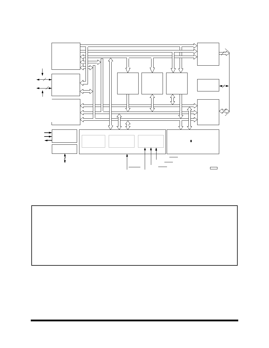
Figure 1 DSP56166 Block Diagram
XDB
PDB
GDB
4
7+10
ADDRESS
POR
T A
PROGRAM CONTROL UNIT
MODA/IRQA
MODB/IRQB
ON-CHIP
PERIPHERALS
HOST, RSSI0,
RSSI1, TIMER
GPI/O, CODEC
INTERNAL DATA
BUS SWITCH
AND BIT
MANIPULATION
UNIT
EXTERNAL
ADDRESS
BUS
SWITCH
BUS
CONTROL
EXTERNAL
DATA BUS
SWITCH
BOOTSTRAP
ROM
64x16
PROGRAM
RAM
2Kx16
DATA
RAM
4Kx16
PROGRAM
ADDRESS
GENERATOR
PROGRAM
DECODE
CONTROLLER
PROGRAM
INTERRUPT
CONTROLLER
DATA ALU
16x16+40 - 40-BIT MAC
TWO 40-BIT ACCUMULATORS
CLOCK
AND PLL
EXTAL
PORT B
OR
HOST
15
CODEC,
PORT C
AND/OR
RSSI0,
RSSI1,
TIMER
RESET
16 BITS
DATA
10
OnCE
SXFC
CLKO
XAB1
XAB2
PAB
ADDRESS
GENERATION
UNIT
16
16
MODC/IRQC
In the USA:
For technical assistance call:
DSP Applications Helpline (512) 891-3230
For availability and literature call your local Motorola Sales Office or Authorized Distributor.
For free application software and information call the Dr. BuB electronic bulletin board:
9600/4800/2400/1200/300 baud
(512) 891-3771
(8 data bits, no parity, 1 stop)
In Europe, Japan and Asia Pacific
Contact your regional sales office or Motorola distributor.
Note
: For the ROM part only (DSP56166ROM) -- Since the on-chip XROM is only connected to the XAB1 address
bus, the data located in this ROM is only accessible by the
first
read of a single read instruction or the
first
read
of a dual parallel read instruction. Therefore, during development using the RAM based part, the data to be
mapped in the on-chip XROM on the ROM based part
should not
be accessed with a
second
read during a
dual parallel read instruction.
2
DSP56166 Technical Data Sheet
MOTOROLA

3
DSP56166
MOTOROLA
PRELIMINARY
INTRODUCTION
This data sheet is intended to be used with the
DSP56100 Fam-
ily Manual
and the
DSP56166 User's Manual
. The
DSP56100
Family Manual
provides a description of the components of the
DSP5616 core processor that are common to all DSP56100 fam-
ily processors and includes a detailed description of the basic
DSP56100 family instruction set. The
DSP56166 User's Manual
provides a description of the memory and peripherals that are
specific to the DSP56166. The
DSP56166 Data Sheet
provides
electrical specifications and timings that are specific to the
DSP56166.
The DSP56166 pinout is shown in Figure 3. The input and output
signals on the chip are organized into the 13 functional groups
shown in Table 1.
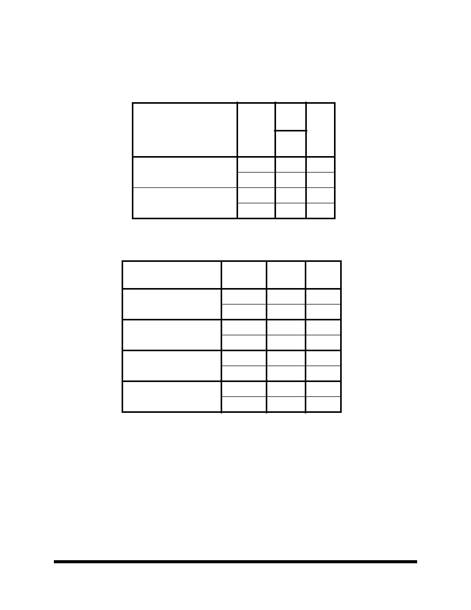
Table 1
Functional Group Pin Allocations
ADDRESS AND DATA BUS (32 PINS
A0-A15
(Address Bus) -- three state, active high outputs. A0-
A15 change in t0 and specify the address for external
program and data memory accesses. If there is no external
bus activity, A0-A15 remain at their previous values. A0-
A15 are three-stated during hardware reset, stop mode and
when the DSP is not the bus master.
D0-D15
(Data Bus) -- three state, active high, bidirectional
input/outputs. Read data is sampled on the trailing edge of
t2, while write data output is enabled by the leading edge of
t2 and three-stated at the leading edge of t0. If there is no
external bus activity, D0-D15 are three-stated. D0-D15 are
also three-stated during hardware reset.
BUS CONTROL (10 PINS)
PS/DS
(Program /Data Memory Select) -- three state active
low output. This output is asserted only when external data
memory is referenced. PS/DS timing is the same for the A0-
Functional Group
Number of Pins
Address and Data Buses
32
Bus Control
10
Interrupt and Mode Control
4
Clock and PLL
3
Host Interface or PIO
15
Timer Interface or PIO
2
RSSI Interfaces or PIO
8
On-chip CODEC
7
On-chip emulation (OnCE)
4
Power (Vdd)
9
Ground (Vss)
16
APower (Vdda)
1
AGround (Vssa)
1
Total 112
A15 address lines. PS/DS is high for program memory
access and is low for data memory access. If the external
bus is not used during an instruction cycle (t0,t1,t2,t3),
PS/DS goes high in t0. PS/DS is in the high impedance
state during hardware reset, stop mode and when the DSP
is not the bus master.
PEREN
(Peripheral Enable) -- three state active low output.
This output is asserted only when external peripheral space
of the data memory is referenced (any address between
X:$FF00 and X:$FF7F). PEREN timing is the same as the
A0-A15 address lines; it is asserted and deasserted during
t0. PEREN is high for any program memory access and for
data memory access not in the space X:$FF00 - X:$FF7F.
PEREN is in the high impedance state during hardware
reset, stop mode and when the DSP is not the bus master.
R/W
(Read/Write)- three state, active low output. Timing is
the same as for the address lines, providing an "early write"
signal. R/W (which changes in t0) is high for a read access
and is low for a write access. If the external bus is not used
during an instruction cycle (t0,t1,t2,t3), R/W goes high in t0.
R/W is three-stated during hardware reset, stop mode and
when the DSP is not the bus master.
WR
(Write Enable) -- three state, active low output. This
output is asserted during external memory write cycles.
When WR is asserted in t1, the data bus pins D0-D15
become outputs and the DSP puts data on the bus during
the leading edge of t2. When WR is deasserted in t3, the
external data has been latched inside the external device.
When WR is asserted, it qualifies the A0-A15 and PS/DS
pins. WR can be connected directly to the WE pin of a static
RAM. WR is three-stated during hardware reset, stop mode
and when the DSP is not the bus master.
RD
(Read Enable) -- three state, active low output. This
output is asserted during external memory read cycles.
When RD is asserted in late t0/early t1, the data bus pins
D0-D15 become inputs and an external device is enabled
onto the data bus. When RD is deasserted in t3, the
external data has been latched inside the DSP. When RD
is asserted, it qualifies the A0-A15 and PS/DS pins. RD can
be connected directly to the OE pin of a static RAM or ROM.
RD is three-stated during hardware reset, stop mode and
when the DSP is not the bus master.
BS
(Bus Strobe) -- active low output. Asserted at the start
of a bus cycle (during t0) and deasserted at the end of the
bus cycle (during t2). This pin provides an "early bus start"
signal which can be used as address latch and as an "early
bus end" signal which can be used by an external bus
controller. BS is three-stated during hardware reset, stop
mode and when the DSP is not the bus master.
TA
(Transfer Acknowledge) -- active low input. If there is
no external bus activity, the TA input is ignored by the DSP.
When there is external bus cycle activity, TA can be used
to insert wait states in the external bus cycle. TA is sampled
on the leading edge of the clock. Any number of wait states
from 1 to infinity may be inserted by using TA. If TA is
sampled high on the leading edge of the clock beginning
the bus cycle, the bus cycle will end 2T after the TA has
been sampled low on a leading edge of the clock; if the Bus
Control Register (BCR) value does not program more wait
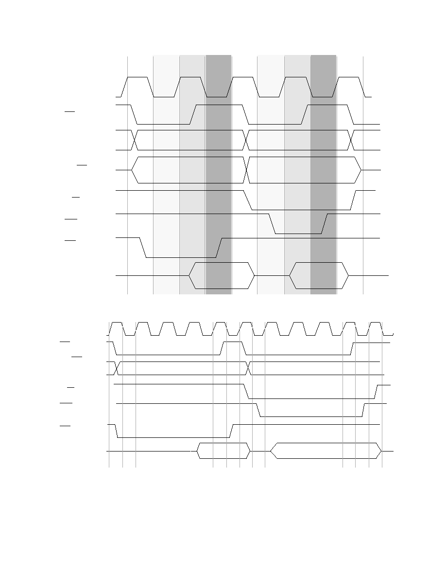
4
MOTOROLA
DSP56166
PRELIMINARY
T0
T1
T2
Tw T2
Tw
T2
Tw
T2
T3
T0
T1
T2
Tw
T2
Tw
T2
Tw
T2
T3
T0 T1
Data in
Data out
CLKO
BS
PS/DS
A0-A15
R/W
WR
RD
D0-D15
T0
T1
T2
T3
T0
T1
T2
T3
T0
Data In
Data Out
CLKO
BS
A0-A15
PS/DS
R/W
WR
RD
D0-D15
Bus Operation (Read-Write- 3WT)
Bus Operation (Read-Write- 0WT)
Figure 2 Bus Operation

5
DSP56166
MOTOROLA
PRELIMINARY
Figure 3 DSP56166 Pinout
MODA/IRQA
MODB/IRQB
MODC/IRQC
RESET
EXTAL
CLKO
SXFC
VddS
GNDS
A0-A15
D0-D15
Vdd Add/Data
Vss Add/Data
BS
PS/DS
PEREN
WR
RD
R/W
TA
BR
BG
BB
Vdd Control
Vss Control
DSI/OS0
DSCK/OS1
DSO
DR
Quiet Vdd
Vss
PB0-PB7
PB8
PB9
PB10
PB11
PB12
PB13
PB14
H0-H7
HA0
HA1
HA2
HR/W
HEN
HREQ
HACK
Vdd Port B
Vss Port B
STD0
SRD0
SCK0
SFS0
STD1
SRD1
SCK1
SFS1
TIN
TOUT
Mic
Aux
SPKP
SPKM
Vrad
Vrda
Vdiv
VddA
VssA
Vdd port C
Vss Port C
PC0
PC1
PC2
PC4
PC5
PC6
PC7
PC9
PC10
PC11
PORT A
Host
Parallel
Interface
On-chip
Emulation
External
Bus
56 pins
(42 func.
5Vdd;9Vss)
Timer
Interrupt
and Mode
Control
Clock
and PLL
8
1
4
1
2
2
1
2
1
1
112 pins
(85 functional pins
16 ground pins
9 power pins
1 Aground pins
1 Apower pin)
Two
Serial
Interfaces
DSP56166
On-chip
Codec
1
1
6
MOTOROLA
DSP56166
PRELIMINARY
states. The number of wait states is determined by the TA
input or by the Bus Control Register (BCR), whichever is
longer. TA is still sampled during the leading edge of the
clock when wait states are controlled by the BCR value. In
that case, TA will have to be sampled low during the leading
edge of the last period of the bus cycle programmed by the
BCR (2T before the end of the bus cycle programmed by
the BCR) in order not to add any wait states. TA should
always be deasserted during t3 to be sampled high by the
leading edge of T0. If TA is sampled low (asserted) at the
leading edge of the t0 beginning the bus cycle, and if no
wait states are specified in the BCR register, zero wait
states will be inserted in the external bus cycle, regardless
the status of TA during the leading edge of T2.
BR
(Bus Request) -- active low output when in master
mode, active low input when in slave mode. This pin is an
input (slave mode) after reset with MODC pin low or when
the bus arbitration mode bit in the OMR register is cleared.
In this mode, the bus request BR allows another device
such as a processor or DMA controller to become the
master of the DSP external data bus D0-D15 and external
address bus A0-A15. The DSP asserts BG a few T states
after the BR input is asserted. The DSP bus controller will
release control of the external data bus D0-D15, address
bus A0-A15 and bus control pins PS/ DS, BS, RD, WR, R/W
and PEREN at the earliest time possible consistent with
proper synchronization. These pins will then be placed in
the high impedance state and the BB pin will be
deasserted. The DSP will continue executing instructions
only if internal program and data memory resources are
being accessed. If the DSP requests the external bus while
BR input pin is asserted, the DSP bus controller inserts wait
states until the external bus becomes available (BR and BB
deasserted). Note that interrupts are not serviced when a
DSP instruction is waiting for the bus controller. Note also
that BR is prevented from interrupting the execution of a
read/ modify/ write instruction.
This pin becomes an output (Master Mode) after reset with
MODC pin high or when the bus arbitration mode bit in the
OMR register is set. In this mode, the DSP is not the
external bus master and has to assert BR to request the
bus mastership. The DSP bus controller will insert wait
states until BG input is asserted and will then begin normal
bus accesses after the rising of the clock which sampled BB
high. The BR output signal will remain asserted until the
DSP no longer needs the bus. In this mode, the Request
Hold bit (RH) of the Bus Control Register (BCR) allows BR
to be asserted under software control.
During external accesses caused by an instruction
executed out of external program memory, BR remains
asserted low for consecutive external memory accesses.
In the master mode, BR can also be used for non arbitration
purpose: if BG is always asserted, BR is asserted in t0 of
every external bus access. It can then be used as a chip
select to turn a external memory device off and on between
internal and external bus accesses. BR timing is in that
case similar to A0-A15, R/W and PS/DS; it is asserted and
deasserted during t0.
BG
(Bus Grant) -- active low input when in master mode,
active low output when in slave mode. Output after power
on reset if the slave mode is selected, this pin is asserted to
acknowledge an external bus request. It indicates that the
DSP will release control of the external address bus A0-
A15, data bus D0-D15 and bus control pins when BB is
deasserted. The BG output is asserted in response to a BR
input. When the BG output is asserted, BB will be
deasserted and the external address bus A0-A15, data bus
D0-D15 and bus control pins will be in the high impedance
state at the end of the current instruction. BG assertion may
occur in the middle of an instruction which requires more
than one external bus cycle for execution. Note that BG
assertion will not occur during indivisible read-modify-write
instructions (BFSET, BFCLR, BFCHG). When BR is
deasserted, the BG output is deasserted and the DSP
Figure 4 TA Controlled Accesses
T0 T1 T2 T3 T0 T1 T2 Tw T2 T3 T0 T1 T2 T3 T0 T1 T2 Tw T2 Tw T2 T3
T0 T1 T2 Tw T2 Tw T2 Tw T2 T3 T0 T1 T2 Tw T2 Tw T2 T3 T0 T1 T2
CLKO
TA
BS
CLKO
TA
BS

7
DSP56166
MOTOROLA
PRELIMINARY
regains control of the external address bus, data bus, and
bus control pins until the BB pin is sampled high.
This pin becomes an input if the bus arbitration mode bit in
the OMR register is set (Master Mode). It is asserted by an
external processor when the DSP may become the bus
master. The DSP can start normal external memory access
after the BB pin has been deasserted by the previous bus
master. When BG is deasserted, the DSP will release the
bus as soon as the current transfer is completed. The state
of BG may be tested by testing the BS bit in the Bus Control
Register.
BG is ignored during hardware reset.
BB
(Bus Busy) -- active low input when not bus master,
active low output when bus master. This pin is asserted by
the DSP when it becomes the bus master and it performs
an external access. It is deasserted when the DSP releases
bus mastership. BB becomes an input when the DSP is no
longer the bus master.
INTERRUPT AND MODE CONTROL (4 PINS)
MODA/IRQA
(Mode Select A/External Interrupt Request A)
-- This input has two functions - to select the initial chip
operating mode and, after synchronization, to allow an
external device to request a DSP interrupt. MODA is read
and internally latched in the DSP when the processor exits
the reset state. MODA and MODB select the initial chip
operating mode. Several clock cycles after leaving the reset
state, the MODA pin changes to the external interrupt
request IRQA. The chip operating mode can be changed by
software after reset. The IRQA input is a synchronized
external interrupt request which indicates that an external
device is requesting service. It may be programmed to be
level sensitive or negative edge triggered. If level sensitive
triggering is selected, an external pull up resistor is required
for wired-OR operation. If the processor is in the stop
standby state and IRQA is asserted, the processor will exit
the stop state.
MODB/IRQB
(Mode Select B/External Interrupt Request B)
-- This input has two functions - to select the initial chip
operating mode and, after internal synchronization, to allow
an external device to request a DSP interrupt. MODB is
read and internally latched in the DSP when the processor
exits the reset state. MODA and MODB select the initial
chip operating mode. Several clock cycles after leaving the
reset state, the MODB pin changes to the external interrupt
request IRQB. After reset, the chip operating mode can be
changed by software. The IRQB input is an external
interrupt request which indicates that an external device is
requesting service. It may be programmed to be level
sensitive or negative edge triggered. If level sensitive
triggering is selected, an external pull up resistor is required
for wired-OR operation.
MODC/IRQC
(Mode Select C/External Interrupt Request C)
-- This input has two functions - to select the initial bus
operating mode and after internal synchronization, to allow
an external device to request a DSP interrupt. MODC is
read and internally latched in the DSP when the processor
exits the RESET state.When tied high, the external bus is
programmed in the master mode (BR output and BG input)
and when tied low the bus is programmed in the slave mode
(BR input and BG output). After RESET, the bus operating
mode can be changed by software writing the MC bit of the
OMR register. Several clock cycles after leaving the
RESET state, the MODC pin changes to the external
interrupt request IRQC. The IRQC input is an external
interrupt request which indicates that an external device is
requesting service. It may be programmed to be level
sensitive or negative edge triggered. If level sensitive
triggering is selected, an external pull up resistor is required
for wired-OR operation.
RESET
(Reset) -- This input is a direct hardware reset of the
processor. When RESET is asserted, the DSP is initialized
and placed in the reset state. A Schmitt trigger input is used
for noise immunity. When the reset pin is deasserted, the
initial chip operating mode is latched from the MODA and
MODB pins. The internal reset signal is deasserted
synchronously with the internal clocks.
POWER, GROUND, AND CLOCK (28
PINS)
VDD (8)
(Power) -- power pins.
VSS (15)
(Ground) -- ground pins.
VDDS
(Synthesizer Power) -- This pin supplies a quiet
power source to the PLL to provide greater frequency
stability.
GNDS
(Synthesizer Ground) -- This pin supplies a quiet
ground source to the PLL to provide greater frequency
stability.
VDDA
(Power Supply input) -- This pin is the positive analog
supply input. It should be connected to VCC when the
codec is not used.
VSSA
(Analog Ground) -- This pin is the analog ground
return. It should be connected to VSS when the codec is not
used.
EXTAL
(External Clock/Crystal Input) -- This input should be
connected to an external clock or to an external oscillator.
A sine wave with a minimum swing of 1Vpp can be applied
to this pin. After being squared, the input frequency can be
used as the DSP core internal clock. In that case, it is
divided by two to produce a four phase instruction cycle
clock, the minimum instruction time being two input clock
periods.This input frequency is also used, after division, as
input clock for the on-chip codec and the on-chip phase
locked loop (PLL).
CLKO
(Clock Output) -- This pin outputs a buffered clock
signal. By programming two bits (CS1-CS0) inside the PLL
Control Register (PLCR), the user can select between
outputting a squared version of the signal applied to
EXTAL, a squared version of the signal applied to EXTAL
divided by 2, and a delayed version of the DSP core master
clock. The clock frequency on this pin can be disabled by
setting the Clockout Disable bit (CD; bit 7) of the Operating
Mode Register (OMR). In this case, the pin is driven low
and can be left floating.
SXFC
(External Filter Capacitor) -- This pin is used to add
an external capacitor to the PLL filter circuit. A low leakage
capacitor should be connected between SXFC and VDDS;
it should be located very close to those pins.

8
MOTOROLA
DSP56166
PRELIMINARY
HOST INTERFACE (15 PINS)
H0-H7
(Host Data Bus) -- This bidirectional data bus is used
to transfer data between the host processor and the DSP.
This bus is an input unless enabled by a host processor
read. H0-H7 may be programmed as general purpose
parallel I/O pins called PB0-PB7 when the Host Interface
(HI) is not being used.
HA0-2
(Host Address 0-2) -- These inputs provide the
address selection for each HI register and should be stable
when HEN is asserted. HA0-HA2 may be programmed as
general purpose parallel I/O pins called PB8-PB10 when
the HI is not being used.
HR/W
(Host Read/Write) -- This input selects the direction of
data transfer for each host processor access. If HR/W is
high and HEN is asserted, H0-H7 are outputs and DSP
data is transferred to the host processor. If HR/W is low and
HEN is asserted, H0-H7 are inputs and host data is
transferred to the DSP. HR/W should be stable when HEN
is asserted. HR/W may be programmed as a general
purpose I/O pin called PB11 when the HI is not being used.
HEN
(Host Enable) -- This input enables a data transfer on
the host data bus. When HEN is asserted and HR/W is
high, H0-H7 becomes an output and DSP data may be
latched by the host processor. When HEN is asserted and
HR/W is low, H0-H7 is an input and host data is latched
inside the DSP when HEN is deasserted. Normally a chip
select signal derived from host address decoding and an
enable clock is connected to the Host Enable. HEN may be
programmed as a general purpose I/O pin called PB12
when the HI is not being used.
HREQ
(Host Request) -- This open-drain output signal is
used by the HI to request service from the host processor.
HREQ may be connected to an interrupt request pin of a
host processor, a transfer request of a DMA controller, or a
control input of external circuitry. HREQ is asserted when
an enabled request occurs in the HI. HREQ is deasserted
when the enabled request is cleared or masked, DMA
HACK is asserted, or the DSP is reset. HREQ may be
programmed as a general purpose I/O pin (not open-drain)
called PB13 when the HI is not being used.
HACK
(Host Acknowledge) -- This input has two functions -
(1) to provide a Host Acknowledge signal for DMA transfers
or (2) to control handshaking and to provide a Host Interrupt
Acknowledge compatible with MC68000 family processors.
If programmed as a Host Acknowledge signal, HACK may
be used as a data strobe for HI DMA data transfers. If
programmed as an MC68000 Host Interrupt Acknowledge,
HACK is used to enable the HI Interrupt Vector Register
(IVR) onto the Host Data Bus H0-H7 if the Host Request
HREQ output is asserted. In this case, all other HI control
pins are ignored and the HI state is not affected. HACK may
be programmed as a general purpose I/O pin called PB14
when the HI is not being used.
16-BIT TIMER (2 PINS)
TIN
(Timer input) -- This input receives external pulses to
be counted by the on-chip 16-bit timer when external
clocking is selected. The pulses are internally synchronized
to the DSP core internal clock. TIN may be programmed as
a general purpose I/O pin called PC10 when the external
event function is not being used.
TOUT
(Timer output) -- This output generates pulses or
toggles on a timer overflow event or a compare event.
TOUT may be programmed as a general purpose I/O pin
called PC11 when disabled by the timer out enable bits
(TO2-TO0).
SYNCHRONOUS SERIAL INTERFACES
(RSSI0 AND RSSI1) (8 PINS)
STD0/PC0
(RSSI0 Transmit Data) -- This output pin
transmits serial data from the RSSI0 Transmit Shift
Register. STD0 may be programmed as a general purpose
I/O pin called PC0 when the RSSI0 STD0 function is not
being used.
SRD0/PC1
(RSSI0 Receive Data) -- This input pin receives
serial data and transfers the data to the RSSI0 Receive
Shift Register. SRD0 may be programmed as a general
purpose I/O pin called PC1 when the RSSI0 SRD0 function
is not being used.
SCK0/PC2
(RSSI0 Serial Clock) -- This bidirectional pin
provides the serial bit rate clock for the RSSI0 interface.
The clock signal can be continuous or gated and is used by
both the transmitter and receiver. SCK0 may be
programmed as a general purpose I/O pin called PC2 when
the RSSI0 interface is not being used.
SFS0/PC4
(Serial Frame Sync 0) -- This bidirectional pin is
used by the RSSI0 serial interface as frame sync I/O or flag
I/O. The SFS0 is used by both the transmitter and receiver
to synchronize the data transfer of the data. It can be input
or output. SFS0 may be programmed as a general purpose
I/O pin called PC4 when the RSSI0 is not using this pin.
STD1/PC5
(RSSI1 Transmit Data) -- This output pin
transmits serial data from the RSSI1 Transmit Shift
Register. STD1 may be programmed as a general purpose
I/O pin called PC5 when the RSSI1 STD1 function is not
being used.
SRD1/PC6
(RSSI1 Receive Data) -- This input pin receives
serial data and transfers the data to the RSSI1 Receive
Shift Register. SRD1 may be programmed as a general
purpose I/O pin called PC6 when the RSSI1 SRD function
is not being used.
SCK1/PC7
(RSSI1 Serial Clock) -- This bidirectional pin
provides the serial bit rate clock for the RSSI1 interface.
The clock signal can be continuous or gated and is used by
both the transmitter and receiver. SCK1 may be
programmed as a general purpose I/O pin called PC7 when
the RSSI1 interface is not being used.
SFS1/PC9
(Serial Frame Sync 1) -- This bidirectional pin is
used by the RSSI1 serial interface as frame sync I/O or flag
I/O. The SFS1 is used by both the transmitter and receiver
to synchronize the data transfer of the data. It can be input
or output. SFS1 may be programmed as a general purpose
I/O pin called PC9 when the RSSI1 is not using this pin.

9
DSP56166
MOTOROLA
PRELIMINARY
ON-CHIP EMULATION (4 PINS)
DSI/OS0
(Debug Serial Input/Chip Status 0) -- The
DSI/OS0 pin, when an input, is the pin through which serial
data or commands are provided to the OnCE controller.
The data received on the DSI pin will be recognized only
when the DSP has entered the debug mode of operation.
Data must have valid TTL logic levels before the serial clock
falling edge. Data is always shifted into the OnCE serial port
most significant bit (MSB) first. When the DSP is not in the
debug mode, the DSI/OS0 pin is an output and it provides
information about the chip status. It is used in conjunction
with the OS1 pin.
DSCK/OS1
(Debug Serial Clock/Chip Status 1) -- The
DSCK/OS1 pin, when an input, is the pin through which the
serial clock is supplied to the OnCE. The serial clock
provides pulses required to shift data into and out of the
OnCE serial port. Data is clocked into the OnCE on the
falling edge and is clocked out of the OnCE serial port on
the rising edge. When the DSP is not in the debug mode,
the DSCK/OS1pin is an output and it provides information
about the chip status. It is used in conjunction with the OS0
pin.
DSO
(Debug Serial Output) -- The debug serial output
provides the data contained in one of the OnCE controller
registers as specified by the last command received from
the command controller. When idle, this pin is high. When
the requested data is available, the DSO line will be
asserted (negative true logic) for nine T cycles (more than
two instruction cycles) to indicate that the serial shift
register is ready to receive clocks in order to deliver the
data. When the chip enters the debug mode due to an
external debug request (DR), an internal software debug
request (DEBUG), a hardware breakpoint occurrence or a
trace/step occurrence, this line will be asserted for eight T
cycles to indicate that the chip has entered the debug mode
and is waiting for commands. Data is always shifted out the
OnCE serial port most significant bit (MSB) first.
DR
(Debug Request Input) -- The debug request input
provides a means of entering the debug mode of operation.
This pin when asserted (negative true logic) will cause the
DSP to finish the current instruction being executed, enter
the debug mode, and wait for commands to be entered
from the debug serial input line.
ON-CHIP CODEC (7 PINS)
AUX
(Auxiliary input) -- This pin is selected as the analog
input to the A/D converter when the INS bit is set in the
codec control register COCR. This pin should be left
floating when the codec is not used.
BIAS
(Bias current pin) -- This input is used to determine
the bias current for the analog circuitry. Connecting a
resistor between BIAS and VGNDA will program the current
bias generator. This pin should be left floating when the
codec is not used.
MIC
(Microphone input) -- This pin is selected as the
analog input to the A/D converter when the INS bit is
cleared in the codec control register COCR. This pin should
be left floating when the codec is not used.
SPKP
(Speaker Positive Output) -- This pin is the positive
analog output from the on-chip D/A converter. This pin
should be left floating when the codec is not used.
SPKM
(Speaker Negative Output) -- This pin is the negative
analog output from the on-chip D/A converter. This pin
should be left floating when the codec is not used.
VRAD
(Voltage Reference Output for the A/D) -- This pin is
the output of the op-amp buffer in the reference voltage
generator for the A/D section. It has a value of (2/5) VDDA.
This voltage is used for analog ground internal to the
block.This pin should always be connected to the Ground
through two capacitors, even when the codec is not used.
VRDA
(Voltage Reference Output for the D/A) -- This pin is
the output of the op-amp buffer in the reference voltage
generator for the D/A section. It has a value of (2/5) VDDA.
This voltage is used for analog ground internal to the
block.This pin should always be connected to the Ground
through two capacitors, even when the codec is not used.
VDIV
(Voltage Division Output) -- This pin is the input to the
op-amp buffer in the reference voltage generator. It is
connected to a resistor divider network located within the
codec block which provides a voltage equal to (2/5)VDDA.
This pin should be connected to the ground via a capacitor
when the codec is used and should be left floating when the
codec is not used.

10
MOTOROLA
DSP56166
PRELIMINARY
PINOUT AND PACKAGE INFORMATION
TOP VIEW
PIN 1
IDENT
29
MOTOROLA
DSP56166
112 CQFP PACKAGE
PIN-OUT
1
28
56
57
84
85
112
PIN #
FUNCTION
1
GND4
2
D2
3
D3
4
VDD3
5
D4
6
D5
7
GND5
8
D6
9
D7
10
D8
11
D9
12
GND6
13
D10
14
D11
15
VDD4
16
D12
17
D13
18
GND7
19
D14
20
D15
21
TA
22
DR
23
VDDA
24
SPKP
25
SPKM
26
GNDA
27
VDIV
28
VRDA
PIN #
FUNCTION
29
MIC
30
AUX
31
VRAD
32
BG
33
QVDD0
34
BR
35
BB
36
VDD5
37
WR
38
GND8
39
RD
40
PS/DS
41
BS
42
R/W
43
DSO
44
DSCK/OS1
45
DSI/OS0
46
CLKO
47
QGND0
48
GNDS
49
XFC
50
VDDS
51
EXTAL
52
SFS1/PC9
53
GND9
54
PEREN
55
SCK1/PC7
56
H7/PB7
PIN #
FUNCTION
57
H6/PB6
58
H5/PB5
59
VDD6
60
H2/PB2
61
H3/PB3
62
H4/PB4
63
SRD1/PC6
64
STD1/PC5
65
H1/PB1
66
H0/PB0
67
HREQ/PB13
68
HACK/PB14
69
HEN/PB12
70
HRW/PB11
71
HA2/PB10
72
HA1/PB9
73
GND10
74
HA0/PB8
75
TOUT/PC11
76
VDD7
77
TIN/PC10
78 SFS0/PC4
79
GND11
80
SCK0/PC2
81
SRD0/PC1
82
STD0/PC0
83
RESET
84
MODA
PIN #
FUNCTION
85
MODB
86
MODC
87
A0
88
A1
89
GND0
90
A2
91
A3
92
VDD1
93
A4
94
A5
95
GND1
96
QVDD1
97
A6
98
A7
99
A8
100
A9
101
GND2
102
A10
103
VDD2
104
QGND1
105
A11
106
A12
107
A13
108
GND3
109
A14
110
A15
111
D0
112
D1
Internal
A0-A15
D0-D15
Bus control
Port B, Once, PortC
Codec
Vcc
QVDD0-1
VDD1-2
VDD3-4
VDD5
VDD6,VDD7
VDDA
GND
QGND0-1
GND0-3
GND4-7
GND8
GND9,GND10, GND11
GNDA

PRELIMINARY - 6/15/93
1
DSP56166 Technical Data Sheet
MOTOROLA
APPENDIX E
ELECTRICAL CHARACTERISTICS
AND TIMING
The DSP56166 is fabricated in high density HCMOS with TTL compatible inputs and CMOS compatible out-
puts.
The preliminary DC/AC electrical specifications are generated from design simulations.
These specifications may not be fully tested or guaranteed at this early stage of the product
life cycle. Finalized specifications will be published after complete characterization and de-
vice qualifications have been completed.
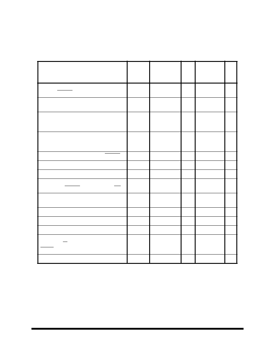
Rating
Symbol
Value
Unit
Supply Voltage
Vdd
-0.3 to +7.0
V
All Input Voltages
V
in
VSS- 0.5 toVdd + 0.5
V
Current Drain per Pin
excluding
Vdd and VSS
I
10
mA
Storage Temperature
T
stg
-55 to +150
∞
C
Maximum Electrical Ratings (VSS = 0 Vdc)
Marking
Speed
Supply Voltage
VDD(V)
Junction Temperature
T
j
(
∞
C)
Min
Max
Min
Max
FE60 60
MHz
4.5
5.5
-40
125
Operating Conditions
PRELIMINARY - 6/15/93
MOTOROLA
DSP56166 Technical Data Sheet
2
This device contains protective circuitry against damage due to high static voltage or electrical fields; how-
ever, it is advised that normal precautions be taken to avoid application of any voltages higher than maxi-
mum rated voltages to this high-impedance circuit. Reliability of operation is enhanced if unused inputs are
tied to an appropriate logic voltage level (e.g., either Vss or Vdd).
Characteristics
Thermal Resistance -- Ceramic
Symbol
Value
Rating
Junction to Ambient
JA
40
∞
C/W
Junction to Case (estimated)
JC
7
∞
C/W
Thermal Characteristics -- CQFP Package
Characteristics
Thermal Resistance -- Plastic
Symbol
Value
Rating
Junction to Ambient
JA
35
∞
C/W
Junction to Case (estimated)
JC
13
∞
C/W
Thermal Characteristics -- PQFP Package

PRELIMINARY - 6/15/93
3
DSP56166 Technical Data Sheet
MOTOROLA
Power Considerations
The average chip junction temperature, T
J
, in
∞
C can be obtained from:
T
J
= T
A
+ (PD*
JA
)
(1)
Where:
T
A
= Ambient Temperature,
∞
C
JA
= Package Thermal Resistance, Junction-to-Ambient,
∞
C/W
P
D
= P
INT
+ P
I/O
PINT = I
CC
*Vdd, Watts -- Chip Internal Power
P
I/O
= Power Dissipation on Input and Output Pins -- User Determined
For most applications P
I/O
< P
INT
and can be neglected. An appropriate relationship between P
D
and T
J
(if
P
I/O
is neglected) is:
P
D
= K/(T
J
+ 273
∞
C)
(2)
Solving equations (1) and (2) for K gives:
K = P
D
*(T
A
+ 273
∞
C) +
JA
*P
D
(3)
Where K is a constant pertaining to the particular part. K can be determined from equation (2) by measuring
P
D
(at equilibrium) for a known T
A
. Using this value of K, the values of P
D
and T
J
can be obtained by solving
equations (1) and (2) iteratively for any value of T
A
. The total thermal resistance of a package (
JA
) can be
separated into two components,
JA
and C
A
, representing the barrier to heat flow from the semiconductor
junction to the package (case) surface (
J
C
) and from the case to the outside ambient (C
A
). These terms
are related by the equation:
JA
=
JC
+ C
A
(4)
JC
is device related and cannot be influenced by the user. However, C
A
is user dependent and can be
minimized by such thermal management techniques as heat sinks, ambient air cooling, and thermal con-
vection. Thus, good thermal management on the part of the user can significantly reduce C
A
so that
JA
ap-
proximately equals
JC
. Substitution of
JC
for
JA
in equation (1) will result in a lower semiconductor junc-
tion temperature. Values for thermal resistance presented in this document, unless estimated, were derived
using the procedure described in Motorola Reliability Report 7843, "Thermal Resistance Measurement
Method for MC68XX Microcomponent Devices", and are provided for design purposes only. Thermal mea-
surements are complex and dependent on procedure and setup. User--derived values for thermal resis-
tance may differ.

PRELIMINARY - 6/15/93
MOTOROLA
DSP56166 Technical Data Sheet
4
Layout Practices
Each DSP56166 Vdd pin should be provided with a low-impedance path to + 5 volts. Each DSP56166 Vss
pin should likewise be provided with a low-impedance path to ground. The power supply pins drive six dis-
tinct groups of logic on chip. They are:
Power and Ground Connections
The VDD power supply should be bypassed to ground using at least six 0.01-0.1 uF bypass capacitors lo-
cated either underneath the chip's socket or as close as possible to the four sides of the package. The ca-
pacitor leads and associated printed circuit traces connecting to chip Vdd and Vss should be kept to less
than 1/2" per capacitor lead. The use of at least a four layer board is recommended, employing two inner
layers as Vdd and Vss planes. All output pins on the DSP56166 have fast rise and fall times. Printed circuit
(PC) trace interconnection length should be minimized in order to minimize undershoot and reflections
caused by these fast output switching times. This recommendation particularly applies to the address and
data buses as well as the PS/DS, BS, RD, WR, R/W, PEREN, IRQA, IRQB, and HEN pins. Maximum PC
trace lengths on the order of 6" are recommended. Capacitance calculations should consider all device
loads as well as parasitic capacitances due to the PC traces. Attention to proper PCB layout and bypassing
becomes especially critical in systems with higher capacitive loads because these loads create higher tran-
sient currents in the Vdd and Vss circuits.
The analog power for the VDDA pin and the analog ground for the VSSA pin should be separated from the
digital VDD and ground planes. The analog power and ground planes should only be tied to the digital power
and ground planes at one point where current enters and exits only at this point.
The analog VDD and ground planes should not have digital signal running over them if possible. The analog
VDD and ground pins should be decoupled as close to the DSP as possible.
Clocks signals should not be run across many signals and should be kept away from analog power and
ground signals as well as any analog signals.
Refer to Analog I/O Figure 1. for more details.
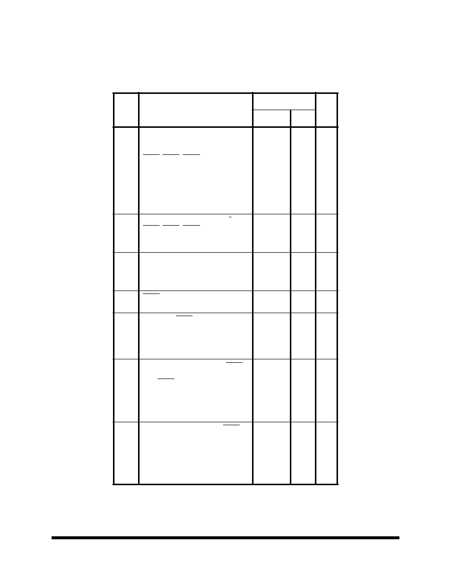
Power and Ground Connections for CQFP and PQFP
Vdd
Vss
Function
33,96
47,104
Internal Logic supply pins
92,103
89,95,101,108
Address bus output buffer supply pins
4,15
1,7,12,18
Data bus output buffer supply pins
36
38
Bus control buffer supply pins
59,76
53,73,79
OnCE, Port B and C output buffer supply pins
23
26
Codec analog supply pins
PRELIMINARY - 6/15/93
5
DSP56166 Technical Data Sheet
MOTOROLA
Power Dissipation
(Vdd = 5.0 Vdc +/- 10%, TJ = -40 to +125
∞
C, CL = 50 pF + 1 TTL Load).
The DC electrical characteristics of this device are shown below.
In order to minimize the power dissipation, all unused digital inputs pins should be tied inactive to VDD or
Vss and all unused I/O pins should be tied inactive through a 10K
resistor to VDD or Vss. All port A input
pins and bydirectional pins must have a valid state at all time when port A is released in order to minimize
power; those pins must then be pulled up or down or driven by another device.
When the codec is not used, VDDA should be connected to VDD and VssA to Vss, and all codec pins should
be left floating except Vref which should still be decoupled.
Conditions
Sym
bol
Typic
al(5V)
Unit
60
MHz
Digital Vdd with
Codec & PLL disabled
IDD
100
mA
PD
500
mW
Digital Vdd WAIT Mode with
CODEC & PLL disabled
IDD
11
mA
PD
55
mW
Conditions
Symbol
Typical
(5V)
Unit
STOP Mode with
PLL and CLKO disabled
IDD
400
µ
A
PD
2
mW
Digital current drawn by
the PLL when active
IDD
2
mA
PD
10
mW
Analog Vdd with
CODEC enabled
IDDA
10
mA
PDA
20
mW
Analog Vdd with
CODEC disabled
IDDA
75
µ
A
PDA
375
µ
W

PRELIMINARY - 6/15/93
MOTOROLA
DSP56166 Technical Data Sheet
6
Analog I/O Characteristics
(VddA = 5.0 Vdc +/- 10%, TJ = -40 to +125
∞
C).
The Analog I/O characteristics of this device are shown below.
a. Min. value reached for a codec clock of 3MHz, typ. for 2MHz and max. for 100KHz
b. 0dBm0 corresponds to 3.14dB below the input saturation level
c. AC coupling is necessary in single-ended mode when the load resistor is not tied to Vref
d.
±
10%
Characteristic
Min
Typ
Max
Unit
Input Impedance on Mic & Aux
a
46
78
1400
k
Input Capacitance on Mic and Aux
--
--
10
pF
Peak Input Voltage on the Mic/Aux Input for Full
Scale Linearity (0.14dBm0
b
): - 6dB- MGS1-0=00
0dB- MGS1-0=01
6dB- MGS1-0=10
17dB- MGS1-0=11
--
--
--
--
--
--
--
--
1.414
0.707
354
100
Vp
Vp
mVp
mVp
Internal Input GainVariation;
G=-6dB, 0dB,6dB or 17dB
(
±
0.83dB variation due to 10% variation on Vdd):
G-0.83
G
G+0.83
dB
Vref Output Voltage
1.8
2
2.2
V
Vref Output Current
--
--
±
1
mA
DC offset between Spkout1 and Spkout2
--
--
100
mV
Allowable Differential Load Capacitance on
Spkout1/2(with 1k
in series)
0
--
50
nF
Allowable Single-ended Load Capacitance on
Spkout1/2(with 0.5k
in series)
0
c
--
100
nF
Maximum Single-ended Signal Output Level
--
--
1
Vp
Maximum Differential Signal Output Level
--
--
2
Vp
Single-ended Load Resistance
500
--
--
Differential Load Resistance
1
--
--
k
R bias
--
10
d
--
k
Internal Output Volume Control Variation
VC=-20,-15,-10,-5,0,6,12,18,24,30,35 dB
(
±
0.83dB variation due to 10% variation on Vdd)
VC-0.83
VC
VC+0.83
dB

PRELIMINARY - 6/15/93
7
DSP56166 Technical Data Sheet
MOTOROLA
Analog I/O Figure 1. describes the recommended analog I/O and power supply configurations.
The two analog inputs are electrically identical. When one is not used, it can be left floating. When used, an
AC coupling capacitor is required. The value of the capacitor along with the input impedance of the pin de-
termine the cut off frequency of a high pass filter. The input impedance of the MIC and AUX varies as a
function of the
modulator master clock. 78 k
is a typical value at 2MHz. An AC capacitor of 1
µ
F defines
a high pass filter pole of 2 Hz. A smaller capacitor value will move this pole higher in frequency.
Analog I/O Figure 1. Recommended Analog I/O Configuration
Vrad
modulator
2.0V
±
10%
Mic
Vrda
Aux
-6dB
6dB
MGS1-0 bits
2 POLE
LPF
VC3-VC0
MAX
Spkp
2Vp
(2/5 Vdd)
Spkm
(MAX 1Vp
when single ended
on 0.5K
)
MUX
INS bit
17dB
Vdiv
1K
50nF
54K
36K
digital Vdd
VddA
VssA
+
15
µ
F
0.1
µ
F
VssA
+5V
+
220
µ
F
Analog Decoupling
near DSP
Single trace
Ext. GND Ext. Supply
GND
digital Vss
Single trace
0.01
µ
F
1
µ
F
600
0.001
µ
F
1
µ
F
600
5.6K
Vrad
0.001
µ
F
5.6K
Vrad
VssA
VddA
( ±
1mA)
+
15
µ
F
0.1
µ
F
VssA
+
15
µ
F
0.1
µ
F
VssA
< 0.1
µ
F
RC

PRELIMINARY - 6/15/93
MOTOROLA
DSP56166 Technical Data Sheet
8
Analog I/O Figure 2. shows three possible single-ended output configurations. Configuration (a) is highly
recommended. For configuration (b) and (c), since the load resistor is tied to VssA, an AC coupling capacitor
is required.
Analog I/O Figure 2. Single-ended Output Configurations
500
Spkp
Spkm
500
47K
47K
47K
Vref
47K
Spkp
Spkm
Spkp
Spkm
500
0<C
100nF
NC
(a)
(b)
(c)
-
+
VddA
VssA
0<C
100nF
0<C
100nF

PRELIMINARY - 6/15/93
9
DSP56166 Technical Data Sheet
MOTOROLA
A/D and D/A Performances
(VddA = 5.0 Vdc +/- 10%, TJ = -40 to +125
∞
C).
The A/D and D/A performances of the codec section are given below.
Analog I/O Figure 3. Example: S/N & S/N+T Performance for the A/D section
a. 0dB gain on the A/D and D/A; Codec clock at 2.048MHz with 128 decimation/interpolation ratio
b. 0dBm0 corresponds to -3.14dB below the input saturation level
Characteristic
Level
Min
.
Typ.
a
Max
.
Unit
Analog to Digital Section Signal to Noise
plus Distortion Ratio (S/N+T)
0dBm0
b
tbd
65
--
dB
-10dBm0
tbd
60
--
dB
-20dBm0
tbd
50
--
dB
-50dBm0
tbd
20
--
dB
Digital to Analog Section Signal to Noise
plus Distortion Ratio (S/N+T)
0dB
tbd
60
--
dB
-10dB
tbd
55
--
dB
-20dB
tbd
45
--
dB
-50dB
tbd
15
--
dB
S in dB
dB
0
10
20
30
40
50
60
70
80
0
-2.86
-5.85
-8.84
-11.85
-14.85
-17.85
-20.86
-23.86
-26.85
-29.89
-32.85
-35.84
-38.85
-41.85
-44.85
-47.8
-50.81
-53.77
-56.76
59.76
-62.83
-65.67
-68.79
-71.91
-74.58
-77.91
S/N
S/N+T

PRELIMINARY - 6/15/93
MOTOROLA
DSP56166 Technical Data Sheet
10
Other On-Chip Codec Characteristics
(VddA = 5.0 Vdc +/- 10%, TJ = -40 to +125
∞
C, CL = 50 pF + 1 TTL Load).
The Analog I/O characteristics of this device are shown below.
Characteristic
Min
Typ
Max
Unit
Codec Master Clock
0.1
2.048
3
MHz
Codec Sampling rate
78
16000
46150
Hz
A/D section settling time
--
--
tbd
msec
D/A section settling time
--
--
tbd
msec
A/D section group delay
--
--
0.2
msec
D/A section group delay
--
--
0.2
msec
A/D to D/A Crosstalk
--
--
tbd
dB
D/A to A/D Crosstalk
--
--
tbd
dBm0
Idle noise at the D/A output
--
--
tbd
µ
Vrms
Idle noise at the A/D digital output
--
--
tbd
dBm0
PRELIMINARY - 6/15/93
11
DSP56166 Technical Data Sheet
MOTOROLA
DC Electrical Characteristics (VSS = 0 Vdc)
(Vdd = 5.0 Vdc +/- 10%, TJ = -40 to +125
∞
C, CL = 50 pF + 1 TTL Load).
The DC electrical characteristics of this device are shown below.
NOTES:
1. When EXTAL is AC coupled, VIHC - VILC
1V must be true.
2. Input capacitance is periodically sampled and not 100% tested in production.
Characteristic
Symbol
Min
Typ
Max
Un
it
Input High Voltage Except
EXTAL, RESET, MODA, MODB,MODC
VIH
2.0
--
Vdd
V
Input Low Voltage Except
EXTAL, MODA, MODB, MODC
VIL
-0.5
--
0.8
V
Input High Voltage
EXTAL DC coupled
EXTAL AC coupled (see note 1)
VIHC
70% of Vdd
1
--
--
Vdd
Vdd
V
Input Low Voltage
EXTAL DC coupled
EXTAL AC coupled (see note 1)
VILC
-0.5
-0.5
--
--
20% of Vdd
Vdd-1
V
Input High Voltage
RESET VIHR
2.5
--
Vdd
V
Input High Voltage MODA , MODB, MODC
VIHM
3.5
--
Vdd
V
Input Low Voltage MODA , MODB, MODC
VILM
-0.5
--
2.0
V
Input Leakage Current
EXTAL, RESET, MODA, MODB, BR
Iin
-1
--
1
uA
Three-State (Off-State) Input Current
(@2.4 V/0.5 V)
TSI
-10
--
10
uA
Output High Voltage
(IOH = -10 uA)
VOHC
Vdd -0.1
--
--
V
Output High Voltage
(IOH = -0.4 mA)
VOH
2.4
--
--
V
Output Low Voltage
(IOL = 10 uA)
VOLC
--
--
0.1
V
Output Low Voltage
(IOL = 3.2 mA;
R/W IOL = 1.6 mA; Open Drain
HREQ IOL = 6.7 mA, TXD IOL = 6.7 mA)
VOL
--
--
0.4
V
Input Capacitance
(see Note 2)
Cin
--
10
--
pF

PRELIMINARY - 6/15/93
MOTOROLA
DSP56166 Technical Data Sheet
12
AC Electrical Characteristics (VSS = 0 Vdc)
The timing waveforms in the AC Electrical Characteristics are tested with a VIL maximum of 0.5 V and a
VIH minimum of 2.4 V for all pins, except EXTAL, RESET, MODA, MODB and MODC. These five pins are
tested using the input levels set forth in the DC Electrical Characteristics. AC timing specifications which
are referenced to a device input signal are measured in production with respect to the 50% point of the re-
spective input signal's transition. The DSP56166 output levels are measured with the production test ma-
chine VOL and VOH reference levels set at 0.8 V and 2.0 V respectively.
AC Electrical Characteristics -- Clock Operation Timing
The system clock to the DSP56166 must be externally supplied to EXTAL.
Notes:
1.
Rise and Fall time may be relaxed to 12 ns maximum if the EXTAL input frequency is less than or
equal to 20MHz. If the EXTAL input frequency is between 20MHz and 40MHz, Rise and Fall time
should be 4 ns maximum. If the EXTAL input frequency is between 40MHz and 60MHz, Rise and
Fall time should meet the specified values in the 40MHz column (3 ns maximum).
2.
The duty cycle may be relaxed to 43-57% if the EXTAL input frequency is less than or equal to
20MHz. If the EXTAL input frequency is between 20MHz and 40MHz, the duty cycle should be such
that Th and Tl meet 12 ns minimum . If the EXTAL input frequency is between 40MHz and 60MHz,
the duty cycle should be such that Th and Tl meet the specified values in the 60MHz column (8 ns
minimum) .
3.
T = Icyc / 4 is used in the electrical characteristics. The exact length of each T is affected by the
duty cycle of the external clock input.
4.
Duty cycles and EXTAL widths are measured at the EXTAL input signal midpoint when AC coupled
and at Vdd/2 when not AC coupled.
Num
Characteristics
Sym
60MHz
Unit
Min
Max
1
Frequency of Operation (EXTAL)
f
0
60
MHz
2
Instruction Cycle Time =2Tc
Icyc
33
ns
3
Wait State =Tc =2T
WS
16.6
ns
4
EXTAL Cycle Period
Tc
16.6
ns
5
EXTAL Rise Time (see Note 1)
--
3
ns
6
EXTAL Fall Time (see Note 1)
--
3
ns
7
EXTAL Width High (see Note 2,
3, 4) 48-52% duty cycle
Th
8
ns
8
EXTAL Width Low (see Note 2,
3, 4) 48%-52% duty cycle
Tl
8
ns
EXTAL
VIHC
Midpoint
7
8
4
2
5
6
Th
Tl
90%
10%
VILC

PRELIMINARY - 6/15/93
13
DSP56166 Technical Data Sheet
MOTOROLA
Clock Figure 1. External Clock Timing
AC Electrical Characteristics -- Other Clock and PLL Operation Timing
Clock Figure 2. Clocking Configurations
a. Maximum DSP operating frequency. See Operating Conditions.
b. An AC coupling capacitor is required on EXTAL if the levels are
out of the normal CMOS level range (VILC>20% of Vdd
or VIHC<70% of Vdd).
Characteristics
Min
Max
Unit
PLL Output frequency
10
Max
Fosc
a
MHz
EXTAL Input Clock Amplitude
b
1
Vdd
Vpp
EXTAL
PLL
PLLE=1
PLLE=0
Fosc
ID3-ID0
CLKO
˜
2
internal phase PH0 at Fosc
CS1-CS0
1000pF
SXFC
VDDS
XFC
1
0.01
µ
F
GNDS
0.1
µ
F
100K
˜
1 to
˜
16
VCO
LF
PFD
YD7-YD0
˜
1 to
˜
256
10nF
Notes:
1. Must be a low leakage capacitor and must be located very close to the SXFC and VDDS pins.
PD3-PD0
˜
2
0
to
˜
2
15
PS=0
PS=1

PRELIMINARY - 6/15/93
MOTOROLA
DSP56166 Technical Data Sheet
14
AC Electrical Characteristics
-- Reset, Stop, Wait, Mode Select, and Interrupt Timing
(Vdd = 5.0 Vdc +/- 10%, TJ = -40 to +125
∞
C, CL = 50 pF + 1 TTL Load).
cyc = Clock cycle = 1/2 instruction cycle = 2 T cycles
ws= Number of wait states programmed into external bus access using BCR (WS = 0 - 31
)
Num
Characteristics
60MHz
Unit
Min
Max
10
RESET Assertion to Address,
Data and control signals High
Impedance
--
21
ns
11
Minimum Stabilization Dura-
tion(see Note 1 )OMR bit6=0
OMR bit6=1
600KT
60T
--
--
ns
ns
12
Asynchronous RESET Deas-
sertion to First External
Address Output (see note 7)
16T
18T
+15
ns
13
Synchronous Reset Setup
Time from RESET Deassertion
to Rising Edge of CLKO
5
cyc-2
ns
14
Synchronous Reset Delay
Time from CLKO High to the
First External Access (see note
7)
16T
+3
16T
+16
ns
15
Mode Select Setup Time
4.8
--
ns
16
Mode Select Hold Time
0.8
--
ns
17
Edge-Triggered Interrupt
Request Width
3.7
--
ns
18
Delay from IRQA, IRQB, IRQC
Assertion to External Data
Memory Access Out Valid
- Caused by First Interrupt
Instruction Fetch
- Caused by First Interrupt
Instruction Execution
11T+3
19T+3
--
--
ns
ns
19
Delay from IRQA, IRQB, IRQC
Assertion to General Purpose
22T
--
ns
PRELIMINARY - 6/15/93
15
DSP56166 Technical Data Sheet
MOTOROLA
AC Electrical Characteristics
-- Reset, Stop, Wait, Mode Select, and Interrupt Timing (Continued)
(Vdd = 5.0 Vdc +/- 10%, TJ = -40 to +125
∞
C, CL = 50 pF + 1 TTL Load).
Notes:
1. Circuit stabilization delay is required during reset when using an external clock in two cases:
1) after power-on reset, and
2) when recovering from Stop mode.
Num
Characteristics
60MHz
Unit
Min
Max
21
Delay from General-Purpose Out-
put Valid Caused by the Execution
of the First Interrupt Instruction to
IRQA, IRQB, IRQC Deassertion for
Level Sensitive Fast Interrupts -- If
2nd Interrupt Instruction is:
Single Cycle
(see note 2)
Two Cycles
--
--
cyc-
26
3cyc-
26
ns
ns
22
Synchronous setup time from
IRQA, IRQB, IRQC assertion to
Synchronous falling edge of CLKO
(see note 5, 6)
0
1
ns
23
Falling Edge of CLKO to First Inter-
rupt Vector Address Out Valid after
Synchronous recovery from Wait
State (see Note 3, 5)
27T+
3
27T+
16
ns
24
IRQA Width Assertion to Recover
from STOP State(see note 4)
3.6
--
ns
25
Delay from IRQA Assertion to Fetch
of first instruction (exiting STOP)
OMR bit 6 = 0
(see note1,3)
OMR bit 6 = 1
524303T
+3
47T+3
--
--
ns
ns
28
Duration for Level Sensitive IRQA
Assertion to Cause the Fetch of
First IRQA Interrupt Instruction
(exiting STOP)
(see note1,3)
OMR bit 6 = 0
OMR bit 6 = 1
524303T
47T
--
--
ns
ns
29
Delay from Level Sensitive IRQA
Assertion to First Interrupt Vector
Address Out Valid (exiting STOP)
(see note1, 3)
OMR bit 6 = 0
OMR bit 6 = 1
524303T
+3
47T+3
--
--
ns
ns
PRELIMINARY - 6/15/93
MOTOROLA
DSP56166 Technical Data Sheet
16
2. When using fast interrupts and IRQA and IRQB are defined as level-sensitive, then timings 20 &
21 apply to prevent multiple interrupt service. To avoid these timing restrictions, the negative edge-
triggered mode is recommended when using fast interrupt. Long interrupts are recommended
when using level-sensitive mode.
3. The interrupt instruction fetch is visible on the pins only in Mode 3.
4. The minimum is specified for the duration of an edge triggered IRQA interrupt required to recover
from the STOP state. This is not the minimum required so that the IRQA interrupt is accepted.
5. Timing #22 is for all IRQx interrupts while timing #23 is only when exiting WAIT
6. Timing #22 triggers off T1 in the normal state and off phi1 when exiting the WAIT state.
7. The instruction fetch is visible on the pins only in Mode 2 and Mode 3.
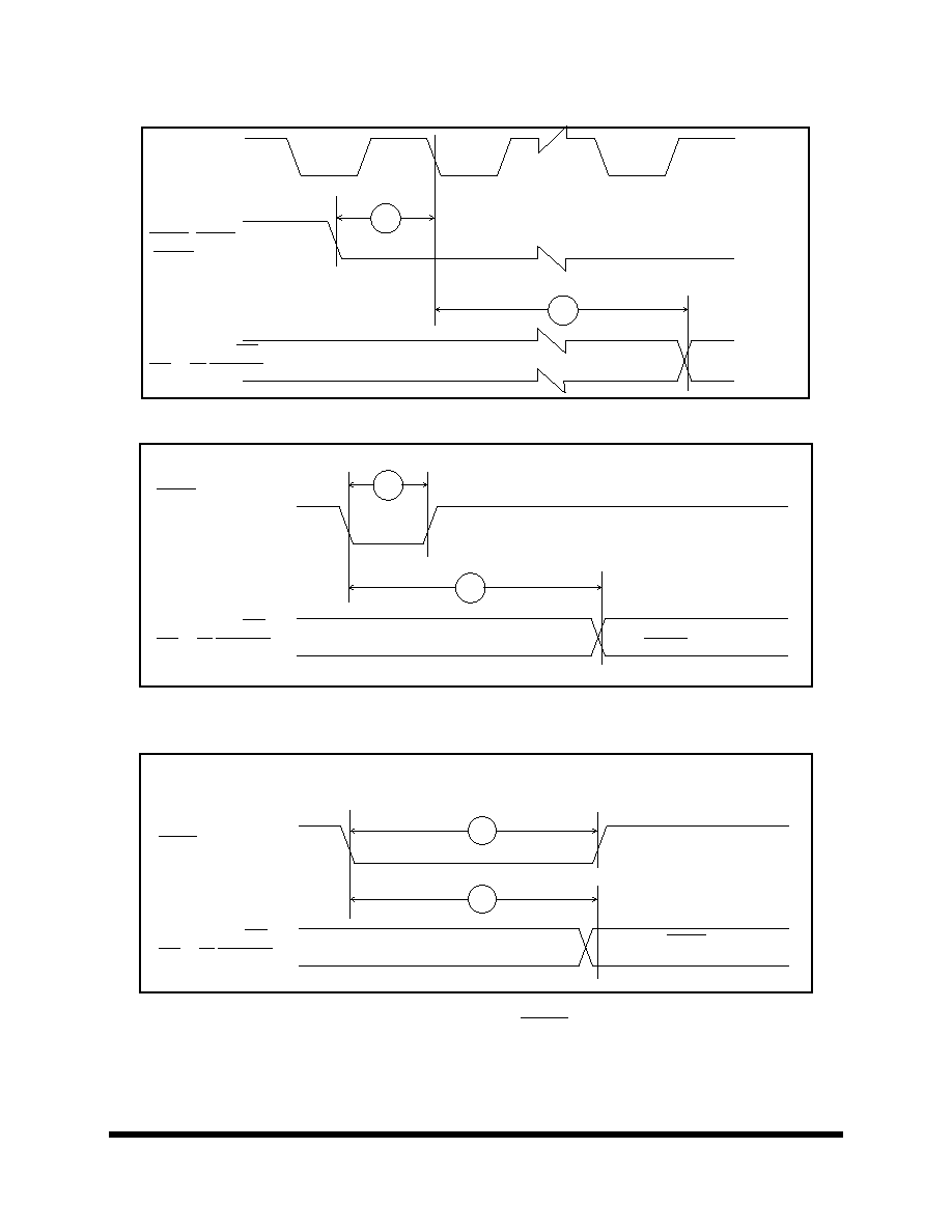
Interrupt Figure 1. Asynchronous Reset Timing
Interrupt Figure 2. Synchronous Reset Timing
Interrupt Figure 3. Operating Mode Select Timing
RESET
D0-D15,
A0-A15,PS/DS
R/W,BS,PEREN
10
11
12
First Fetch
VIHR
CLKO
RESET
A0-A15,
PS/DS, BS,
R/W,PEREN
14
13
RESET
MODA, MODB,
MODC
VIHR
IRQA, IRQB
IRQC
VIHM
VILM
VIH
VIL
16
15

PRELIMINARY - 6/15/93
17
DSP56166 Technical Data Sheet
MOTOROLA
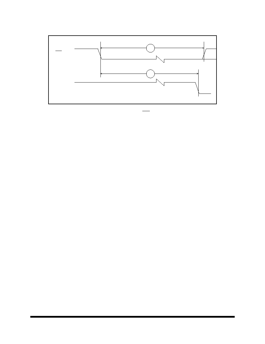
Interrupt Figure 4. External Interrupt Timing (Negative Edge-Triggered)
Interrupt Figure 5. External Level-Sensitive Fast Interrupt Timing
IRQA, IRQB,
IRQC
17
First Interrupt Instruction Execution
A0-A15
PS/DS
BS,
R/W
PEREN
IRQA
IRQB,
IRQC
20
18
a) First Interrupt Instruction Execution
General
Purpose
I/O
IRQA
IRQB,
IRQC
19
21
b) General Purpose I/O
PRELIMINARY - 6/15/93
MOTOROLA
DSP56166 Technical Data Sheet
18
Wait and Stop 1. Synchronous Interrupt from Wait State Timing
Wait and Stop 2.
Recovery from STOP State using Asynchronous Interrupt Timing
Wait and Stop 3.
Recovery from Stop State Using IRQA Interrupt Service
CLKO
IRQA, IRQB,
IRQC
A0-A15, PD/DS
BS,R/W,PEREN
22
23
T0, T2
phi0
Instruction Fetch
First Interrupt
T1, T3
phi1
IRQA
A0-A15, PD/DS
BS,R/W,PEREN
24
25
First Instruction Fetch
Not IRQA Interrupt Vector
IRQA
A0-A15, PD/DS
BS,R/W,PEREN
First IRQA Interrupt
Instruction Fetch
28
29

PRELIMINARY - 6/15/93
19
DSP56166 Technical Data Sheet
MOTOROLA
Wait and Stop 4.
Recovery from WAIT State Using DR Pin-- Synchronous Timing
Num
Characteristics
60MHz
Unit
Min
Max
30
DR Asserted to CLK low (Setup
Time for Synchronous Recovery
from Wait State)
8
cyc+8
ns
31
CLK low to DSO (ACK) Valid
(Enter Debug Mode) After Syn-
chronous Recovery from Wait
State
18cyc
--
ns
AC Electrical Characteristics -- Wait and Stop Timings
(Continued)
CLKO
(output)
DR
(input)
DSO
(output)
31
T0, T2
T1, T3
30
33
PRELIMINARY - 6/15/93
MOTOROLA
DSP56166 Technical Data Sheet
20
Wait and Stop 5.
Recovery from WAIT/STOP State Using DR Pin-- Asynchronous Timing
DR
(input)
DSO
(output)
33
32
33

PRELIMINARY - 6/15/93
21
DSP56166 Technical Data Sheet
MOTOROLA
AC Electrical Characteristics
Capacitance Derating --External Bus Synchronous Timing
VCC = 5.0 Vdc +/- 10%, T
J
= -40 to +125∞ C, CL = 50 pF + 1 TTL Load.
The DSP56166 External Bus Timing Specifications are designed and tested at the maximum capacitive
load of 50 pF, including stray capacitance. Typically, the drive capability of the External Bus pins (A0-A15,
D0-D23, PS/DS, RD, WR, R/W, BS, PEREN) derates linearly at 1 ns per 12 pF of additional capacitance
from 50 pF to 250 pF of loading. Port B and C pins derate linearly at 1 ns per 5 pF of additional capacitance
from 50 pF to 250 pF of loading.
When an internal memory access follows an external memory access, the PS/DS, R/W, RD, WR, BS and
PEREN strobes remain deasserted and A0-A15 do not change from their previous state.

PRELIMINARY - 6/15/93
MOTOROLA
DSP56166 Technical Data Sheet
22
Num
Characteristic
60MHz
Unit
Min
Max
34
CLK in (EXTAL) High to CLKO High
ns
35
CLKO High to
a. A0-A15 Valid
b. PS/DS, PEREN Assertion, R/W Valid
c. BS Assertion
d. RD Assertion
5.8
8.7
8.7
8.3
ns
ns
ns
ns
36
BS Width Deassertion
14.6
--
ns
37
CLKO High to WR Assertion Low
T+
6.0
ns
38
39
40
CLKO High to BS Deassertion
1.5
ns
41
a.TA Assertion to CLKO High (Setup)
b.TA Deassertion to CLKO High (Setup)
5.9
--
--
ns
ns
42
a. CLKO High to TA Assertion (Hold)
b. CLKO High to TA Deassertion (Hold)
8.3
--
--
ns
ns
43
CLKO High to D0-D15 Out Valid
8.8
ns
44
CLKO High to D0-D15 Out Invalid (Hold)
1.6
--
ns
45
D0-D15 In Valid to CLKO Low (Setup)
2.5
--
ns
46
CLKO Low to D0-D15 In Invalid (Hold)
0.1
--
ns
47
CLKO Low to
a. WR Deassertion
b. RD Deassertion
--
--
4.8
4.0
ns
ns
48
a. WR Hold Time from CLKO Low
b. RD Hold Time from CLKO Low
1.6
0.5
--
--
ns
ns
49
CLKO High to D0-D15 Three-state
TBD
ns
50
CLKO High to D0-D15 Out Active
TBD
ns
51
CLKO High to
a. A0-A15 Invalid
b. PS/DS, PEREN ,R/W Invalid
1.1
2.2
ns
ns

PRELIMINARY - 6/15/93
23
DSP56166 Technical Data Sheet
MOTOROLA
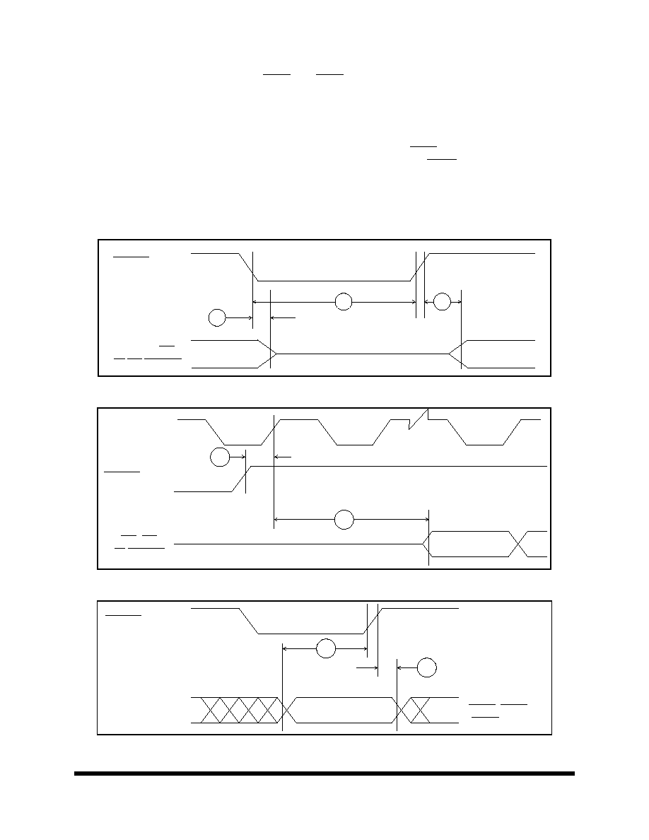
External Bus Figure 1. External Bus Synchronous Timing -- No Wait States
Note 1: During Read-Modify-Write instructions and internal instructions, the address lines do not
change state
EXTAL
(Input)
CLKO
(Output)
A0-A15,
PS/DS,R/W
PEREN
Note 1
BS
(Output)
WR
(Output)
RD
(Output)
TA
(Input)
D0-D15
(Output)
D0-D15
(Input)
T0
T1
T2
T3
T0
T1
T2
Data In
37
35
35
41
43
44
Data Out
34
36
40
42
47
48
51
50
46
49
45
35
47
48
41

PRELIMINARY - 6/15/93
MOTOROLA
DSP56166 Technical Data Sheet
24
External Bus Figure 2. External Bus Synchronous Timing ≠ Two Wait States
EXTAL
(Input)
CLKO
(Output)
A0-A15,
PS/DS,R/W
PEREN
(Outputs)
BS
(Output)
WR
(Output)
RD
(Output)
TA
(Input)
D0-D15
(Output)
D0-D15
(Input)
T0
T1
T2
Tw
T2
Tw
T2
T3
T0
Data In
37
35
35
41
43
44
Data Out
34
36
40
42
47
48
51
50
46
49
45
35
47
48
42
41
PRELIMINARY - 6/15/93
25
DSP56166 Technical Data Sheet
MOTOROLA
AC Electrical Characteristics
External Bus Asynchronous Timing
VCC = 5.0 Vdc +/- 10%, T
J
= -40 to +125∞ C, CL = 50 pF + 1 TTL Load.
cyc = Clock cycle = 1/2 instruction cycle = 2 T cycles
WS = Number of Wait States, Determined by BCR Register (WS = 0 to 31)
WT = WS*cyc=2T*WS
Num
Characteristic
60MHz
Unit
Min
Max
52
WR and RD Deassertion High to BS
Assertion Low (2 Successive Bus Cycles)
TBD
TBD
ns
53
Address Valid to WR Assertion
TBD
TBD
ns
54
WR Width Assertion
WS=0
WS>0
TBD
--
--
ns
55
WR Deassertion to R/W, Address Invalid
TBD
--
ns
56
WR Assertion to D0-D15 Out Valid
TBD
TBD
ns
57
Data Out Hold Time from WR Deassertion
TBD
TBD
ns
58
Data Out Set up Time to WR
WS=0
Deassertion
WS>0
TBD
--
--
ns
59
RD Deassertion to Adress not valid
TBD
--
ns
60
Address valid to RD Deassertion
TBD
--
ns
61
Input data hold to RD Deassertion
TBD
--
ns
62
RD Assertion width
WS=0
WS>0
TBD
--
--
ns
63
Address valid to input data valid WS=0
WS>0
--
--
TBD
ns
64
Address valid to RD Assertion
TBD
ns
65
RD Assertion to input data valid WS=0
WS>0
--
--
TBD
ns
66
WR Deassertion to RD Assertion
TBD
--
ns
67
RD Deassertion to RD Assertion
TBD
--
ns
68
WR Deassertion to WR Assertion
TBD
--
ns
69
RD Deassertion toWR Assertion
TBD
--
ns
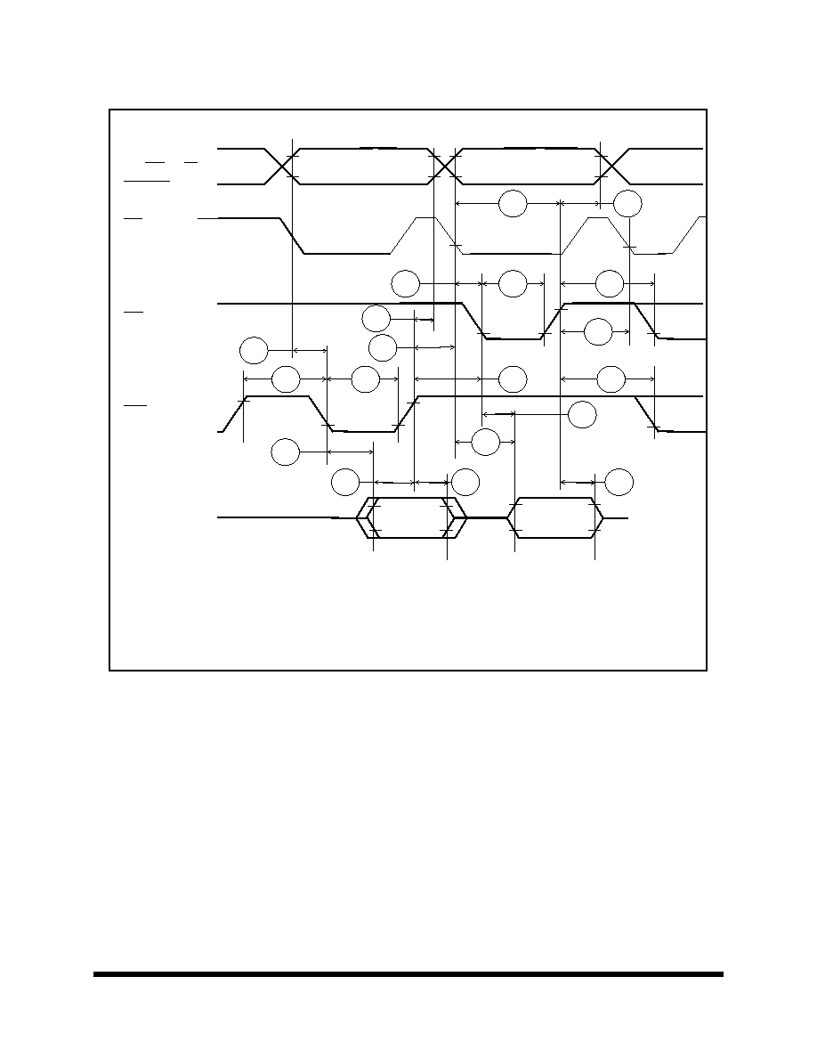
PRELIMINARY - 6/15/93
MOTOROLA
DSP56166 Technical Data Sheet
26
External Bus Figure 3. External Bus Asynchronous Timing
Data In
64
59
Data Out
62
67
68
54
66
69
58
57
63
65
61
55
A0-A15,
PS/DS, R/W
PEREN
BS
RD
WR
D0-D15
53
60
56
Note:
1. During Read-Modify-Write instructions and internal instructions,
the address lines do not change state.
52
52

PRELIMINARY - 6/15/93
27
DSP56166 Technical Data Sheet
MOTOROLA
AC Electrical Characteristics -- Bus Arbitration Timing -- Slave Mode
VCC = 5.0 Vdc +/- 10%, T
J
= -40 to +125∞ C, CL = 50 pF + 1 TTL Load.
cyc = Clock cycle = 1/2 instruction cycle = 2 T cycles
WS = Number of Wait States for X or P external memory , Determined by BCR or BCR2 Registers (WS = 0 to 31)
WT = WS*cyc=2T*WS
Wx = Number of Wait States for X external memory, Determined by BCR or BCR2 Registers (WS = 0 to 31)
Wp = Number of Wait States for P external memory, Determined by BCR Register (WS = 0 to 31)
Num
Characteristics
60 MHz
Unit
Min
Max
70
BR Input to CLKO low setup time
2.8
ns
71
Delay from BR Input Assertion
(See note 1)
to BG Output Assertion
(See note 2)
(See note 3)
(See note 4)
(See note 5)
TBD
TBD
TBD
TBD
TBD
ns
ns
ns
ns
ns
72
CLKO high to BG Output Assertion
7.2
ns
73
BG Output Deassertion duration (See note 1)
for two consecutive BR
(See note 2)
(See note 3)
(See note 4)
(See note 5)
(See note 7)
TBD
TBD
TBD
TBD
TBD
TBD
--
--
--
--
--
--
ns
ns
ns
ns
ns
ns
74
CLKO High to Control Bus high impedance
TBD
ns
75
CLKO High to BB Output Deassertion
10.3
ns
76
CLKO High to BB Output (Three-state)
TBD
ns
77
BR Input Deassertion to
(See note 1)
BG Output Deassertion
(See note 5)
(See note 7)
TBD
TBD
TBD
ns
ns
ns
78
CLKO High to BG Deassertion
2.0
ns
79
CLKO High to BB Output Active
TBD
ns
80
CLKO High to BB Output Assertion
8.5
ns
81
CLKO High to Address and Control Bus Active
TBD
ns
82
CLKO High to Address and Control Bus Valid
8.5
ns

PRELIMINARY - 6/15/93
MOTOROLA
DSP56166 Technical Data Sheet
28
NOTES:
1. With no external access from the DSP56166
2. During external read or write access
3. During external read-modify-write access
4. During STOP mode -- external bus is released and BG is always low
5. During WAIT mode
7. With external accesses pending by the DSP56166
8. Slave mode, when bus is still busy after bus request has been deasserted
Num
Characteristics
60 MHz
Unit
Min
Max
83
BR Assertion to
(See note 1)
BB Deassertion
(See note 2)
(See note 3)
(See note 4)
(See note 5)
TBD
TBD
TBD
TBD
TBD
ns
ns
ns
ns
ns
84
BR Assertion to
(See note 1)
Addr/Data/Control Three-state
(See note 2)
(See note 3)
(See note 4)
(See note 5)
TBD
TBD
TBD
TBD
TBD
ns
ns
ns
ns
ns
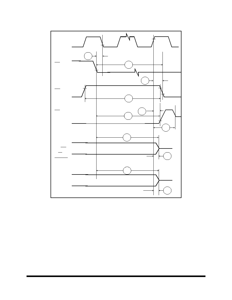
PRELIMINARY - 6/15/93
29
DSP56166 Technical Data Sheet
MOTOROLA
External Bus Figure 4. Bus Arbitration Timing -- Slave Mode -- Bus Release.
72
74
70
71
74
76
75
CLKO
(Output)
BR
(Input)
BG
(Output)
BB
(I/O)
A0-A15,
PS/DS
R/W
PEREN
D0-D15
73
83
84
84
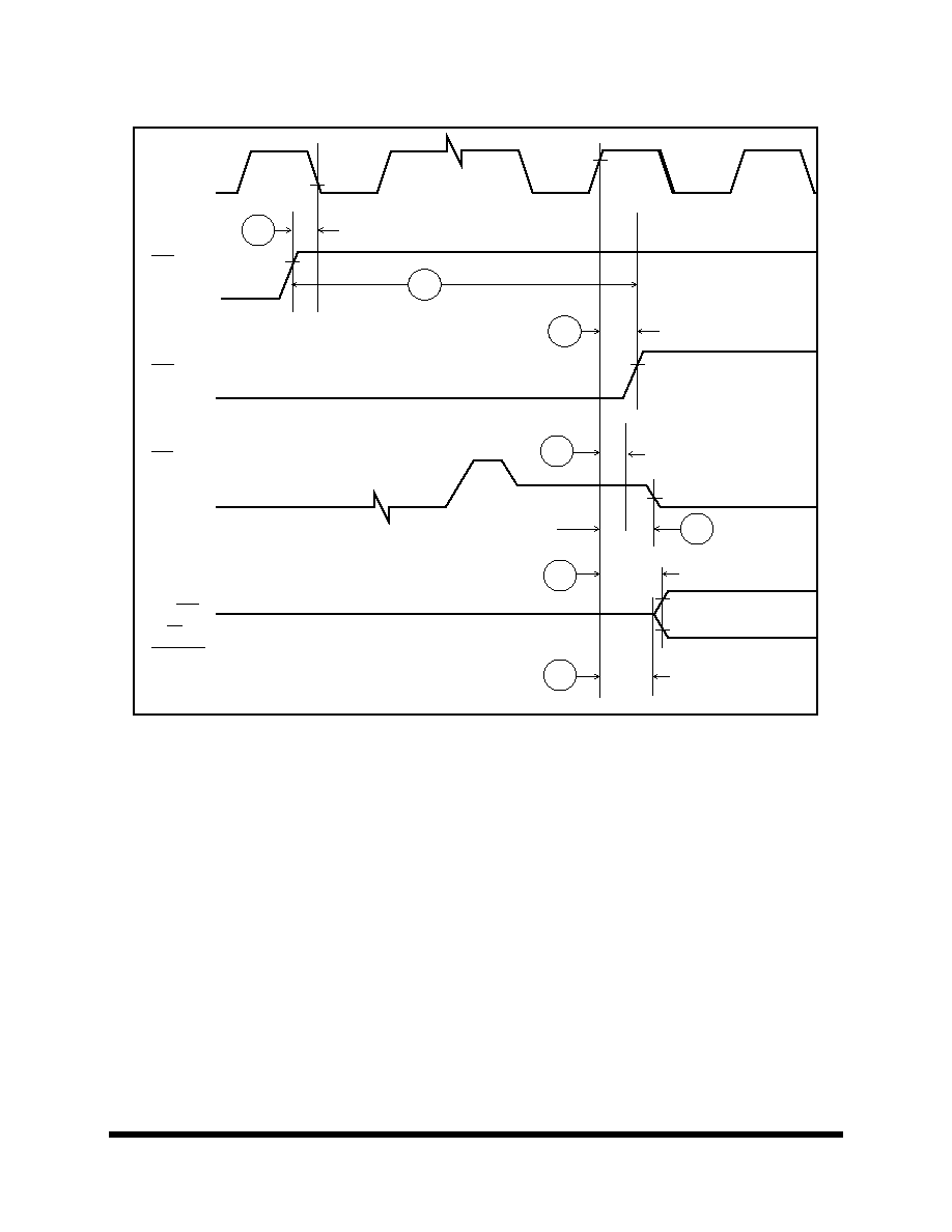
PRELIMINARY - 6/15/93
MOTOROLA
DSP56166 Technical Data Sheet
30
External Bus Figure 5.
Bus Arbitration Timing -- Slave Mode -- Bus Acquisition.
70
78
80
79
77
CLKO
(Output)
BR
(Input)
BG
(Output)
BB
(I/O)
A0-A15,
PS/DS
R/W
PEREN
81
82
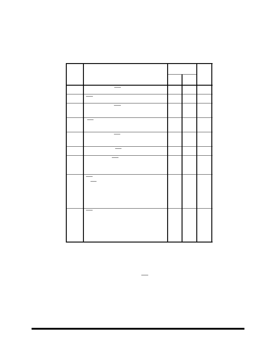
PRELIMINARY - 6/15/93
31
DSP56166 Technical Data Sheet
MOTOROLA
AC Electrical Characteristics -- Bus Arbitration Timing -- Master Mode
VCC = 5.0 Vdc +/- 10%, T
J
= -40 to +125∞ C, CL = 50 pF + 1 TTL Load.
NOTES:
1. With no external access from the DSP56166
2. During external read or write access
3. During external read-modify-write access
4. During STOP mode -- external bus is released and BG is always low
5. During WAIT mode
Num
Characteristic
60MHz
Unit
Min
Max
85
CLKO high to BR Output Valid
7.3
ns
86
BG Input Valid to CLKO Low (Setup)
1.7
--
ns
87
CLKO Low to BG Input Deassertion
(Hold)
TBD
--
ns
88
BB Input Deassertion to CLKO Low
(Setup)
1.5
--
ns
89
CLKO Low to BB Input Deassertion
(Hold)
TBD
--
ns
90
CLKO High to BB Output Assertion
8.0
ns
91
CLKO Low to BG Input Assertion
(See note 1)
(See note 2)
TBD
TBD
--
--
ns
ns
92
BG Deassertion
to BB Deassertion
(See note 1)
(See note 2)
(See note 3)
(See note 4)
(See note 5)
TBD
TBD
TBD
TBD
TBD
ns
ns
ns
ns
ns
93
BG Deassertion to
Addr/Data/Control
(See note 1)
Three-state
(See note 2)
(See note 3)
(See note 4)
(See note 5)
TBD
TBD
TBD
TBD
TBD
ns
ns
ns
ns
ns

PRELIMINARY - 6/15/93
MOTOROLA
DSP56166 Technical Data Sheet
32
External Bus Figure 6.
Bus Arbitration Timing -- Master Mode -- Bus Acquisition.
86
85
89
88
CLKO
(Output)
BR
(Output)
BG
(Input)
BB
(I/O)
A0-A15,
PS/DS
R/W
PEREN
87
90
81
82
Three-state

PRELIMINARY - 6/15/93
33
DSP56166 Technical Data Sheet
MOTOROLA
External Bus Figure 7.
Bus Arbitration Timing -- Master Mode -- Bus Release.
85
86
91
74
CLKO
(Output)
BR
(Output)
BG
(Input)
BB
(I/O)
A0-A15,
D0-D15,
PS/DS, BS,
R/W, RD,
WR,
PEREN
76
75
92
93
Output

PRELIMINARY - 6/15/93
MOTOROLA
DSP56166 Technical Data Sheet
34
HOST PORT USAGE CONSIDERATIONS
Careful synchronization is required when reading multibit registers that are written by another asynchronous
system. This is a common problem when two asynchronous systems are connected. The situation exists in
the Host port. The considerations for proper operation are discussed below.
Host Programmer Considerations
1.
Unsynchronized Reading of Receive Byte Registers
When reading receive byte registers, RXH or RXL, the Host programmer should use interrupts or poll
the RXDF flag which indicates that data is available. This assures that the data in the receive byte
registers will be stable.
2.
Overwriting Transmit Byte Registers
The Host programmer should not write to the transmit byte registers, TXH or TXL, unless the TXDE bit
is set indicating that the transmit byte registers are empty. This guarantees that the transmit byte
registers will transfer valid data to the HRX register.
3.
Synchronization of Status Bits from DSP to Host
HC, HREQ, DMA, HF3, HF2, TRDY, TXDE, and RXDF (refer to DSP56166 User's Manual, I/O Interface
section, Host/DMA Interface Programming Model for descriptions of these status bits) status bits are
set or cleared from inside the DSP and read by the Host processor. The Host can read these status bits
very quickly without regard to the clock rate used by the DSP, but the possibility exists that the state of
the bit could be changing during the read operation. This is generally not a system problem, since the
bit will be read correctly in the next pass of any Host polling routine.
However, if the Host asserts the HEN for more than timing number 101 (T101), with a minimum cycle
time of timing number 103 (T103), then the status is guaranteed to be stable
A potential problem exists when reading status bits HF3 and HF2 as an encoded pair. If the DSP
changes HF3 and HF2 from 00 to 11, there is a small probability that the Host could read the bits during
the transition and receive 01 or 10 instead of 11. If the combination of HF3 and HF2 has significance,
the Host could read the wrong combination.
Solution:
a. Read the bits twice and check for consensus.
b. Assert HEN access for T101a so that status bit transitions are stabilized.
4.
Overwriting the Host Vector
The Host programmer should change the Host Vector register only when the Host Command bit (HC)
is clear. This change will guarantee that the DSP interrupt control logic will receive a stable vector.
5.
Cancelling a Pending Host Command Exception
The Host processor may elect to clear the HC bit to cancel the Host Command Exception request at
any time before it is recognized by the DSP. Because the Host does not know exactly when the
exception will be recognized (due to exception processing synchronization and pipeline delays), the
DSP may execute the Host exception after the HC bit is cleared. For these reasons, the HV bits must
not be changed at the same time the HC bit is cleared.
DSP Programmer Considerations
1.
Reading HF0 and HF1 as an Encoded Pair
DMA, HF1, HF0, and HCP, HTDE, and HRDF (refer to DSP56166User's Manual, I/O Interface section,
Host/DMA Interface Programming Model for descriptions of these status bits) status bits are set or
cleared by the Host processor side of the interface. These bits are individually synchronized to the DSP
clock.
A potential problem exists when reading status bits HF1 and HF2 as an encoded pair, i.e., the four
combinations 00, 01, 10, and 11 each have significance. A very small probability exists that the DSP
will read the status bits synchronized during transition. The solution to this potential problem is to read
the bits twice for consensus.
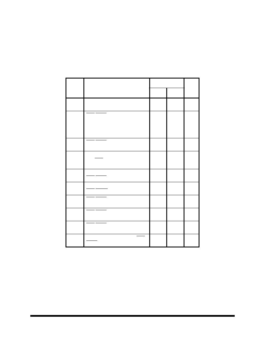
PRELIMINARY - 6/15/93
35
DSP56166 Technical Data Sheet
MOTOROLA
AC Electrical Characteristics -- Host I/O Timing
(VCC = 5.0 Vdc +/- 10%, TJ = -40
∞
to +125
∞
C, CL = 50 pF + 1 TTL Load, see Host Figures 1 through 6)
T = Icyc / 4
cyc=Clock cycle =1/2 instruction cycle= 2 T cycle
tHSDL = Host Synchronization Delay Time
t
suh
: Host processor data setup time
Active low lines should be "pulled up" in a manner consistent with the AC and DC specifications
Num
Characteristic
60MHz
Unit
Min
Max
100
Host Synchronous Delay
(see Note 1)
T
3T
ns
101
HEN/HACK Assertion Width
a.CVR,ICR, ISR Read
(see Note 2,4)
b.Read
c.Write
2T+
30
16+t
suh
8.0
--
--
--
ns
102
HEN/HACK Deassertion Width
(see Note 2)
27
--
ns
103
Minimum Cycle Time Between
Two HEN Assertion for Consecu-
tive CVR, ICR, ISR reads
4T+
30
--
ns
104
Host Data Input Setup Time Before
HEN/HACK Deassertion
3
--
ns
105
Host Data Input Hold Time After
HEN/HACK Deassertion
9
--
ns
106
HEN/HACK Assertion to Output
Data Active from High Impedance
0
--
ns
107
HEN/HACK Assertion to Output
Data Valid
--
24
ns
108
HEN/HACK Deassertion to Output
Data High Impedance
--
17
ns
109
Output Data Hold Time After HEN/
HACK Deassertion
5
--
ns

PRELIMINARY - 6/15/93
MOTOROLA
DSP56166 Technical Data Sheet
36
NOTES:
1. "Host synchronization delay (tHSDL)" is the time period required for the DSP56166 to
sample any external asynchronous input signal, determine whether it is high or low, and
synchronize it to the internal clock.
2. See HOST PORT USAGE CONSIDERATIONS.
3. HREQ is pulled up by 1k
.
4. Only if two consecutive reads from one of these registers are executed.
Num
Characteristic
60MHz
Unit
Min
Max
110
HR/W Low Setup Time Before HEN Asser-
tion
4
--
ns
111
HR/W Low Hold Time After HEN Deasser-
tion
4
--
ns
112
HR/W High Setup Time to HEN Assertion
4
--
ns
113
HR/W High Hold Time After HEN/HACK
Deassertion
3
--
ns
114
HA0-HA2 Setup Time Before HEN Asser-
tion
0
--
ns
115
HA0-HA2 Hold Time After HEN Deassertion
6
--
ns
116
DMA HACK Assertion to HREQ Deasser-
tion(see Note 3)
4
2T+
35
ns
117
DMA HACK Deassertion to HREQ
Assertion(see Note 3)
for DMA RXL Read
for DMA TXL Write
for All Other Cases
t
HSDL
+3T+4
t
HSDL
+2T+4
4
--
--
--
ns
ns
ns
118
Delay from HEN Deassertion to HREQ
Assertion for RXL Read (see Note 3)
t
HSDL
+3T+4
--
ns
119
Delay from HEN Deassertion to HREQ
Assertion for TXL Write (see Note 3)
t
HSDL
+2T+4
--
ns
120
Delay from HEN Assertion to HREQ Deas-
sertion for RXL Read, TXL Write
( see Note 3)
13.7
2T+
16.4
ns
AC Electrical Characteristics -- Host I/O Timing (Continued)

PRELIMINARY - 6/15/93
37
DSP56166 Technical Data Sheet
MOTOROLA
Host Figure 1. Host Synchronization Delay
Host Figure 2. Host Interrupt Vector Register (IVR) Read
EXTERNAL
INTERNAL
100
100
HREQ
(OUTPUT)
HACK
(INPUT)
HR/W
(INPUT)
H0-H7
(OUTPUT)
102
103
112
113
108
107
106
109
Data Valid
101

PRELIMINARY - 6/15/93
MOTOROLA
DSP56166 Technical Data Sheet
38
Host Figure 3. Host Read Cycle (Non-DMA Mode)
Host Figure 4. Host Write Cycle (Non-DMA Mode)
HREQ
(OUTPUT)
HEN
(INPUT)
HA2-HA0
(INPUT)
HR/W
(INPUT)
H0-H7
(OUTPUT)
118
120
103
101
102
114
115
112
113
107
108
106
109
RXL
Read
RXH
Read
Address
Valid
Address
Valid
Data
Valid
Data
Valid
119
120
103
101
102
114
115
TXL
Write
TXH
Write
Address
Valid
Address
Valid
Data
Valid
Data
Valid
HREQ
(OUTPUT)
HEN
(INPUT)
HA2-HA0
(INPUT)
HR/W
(INPUT)
H0-H7
(INPUT)
110
111
104
105
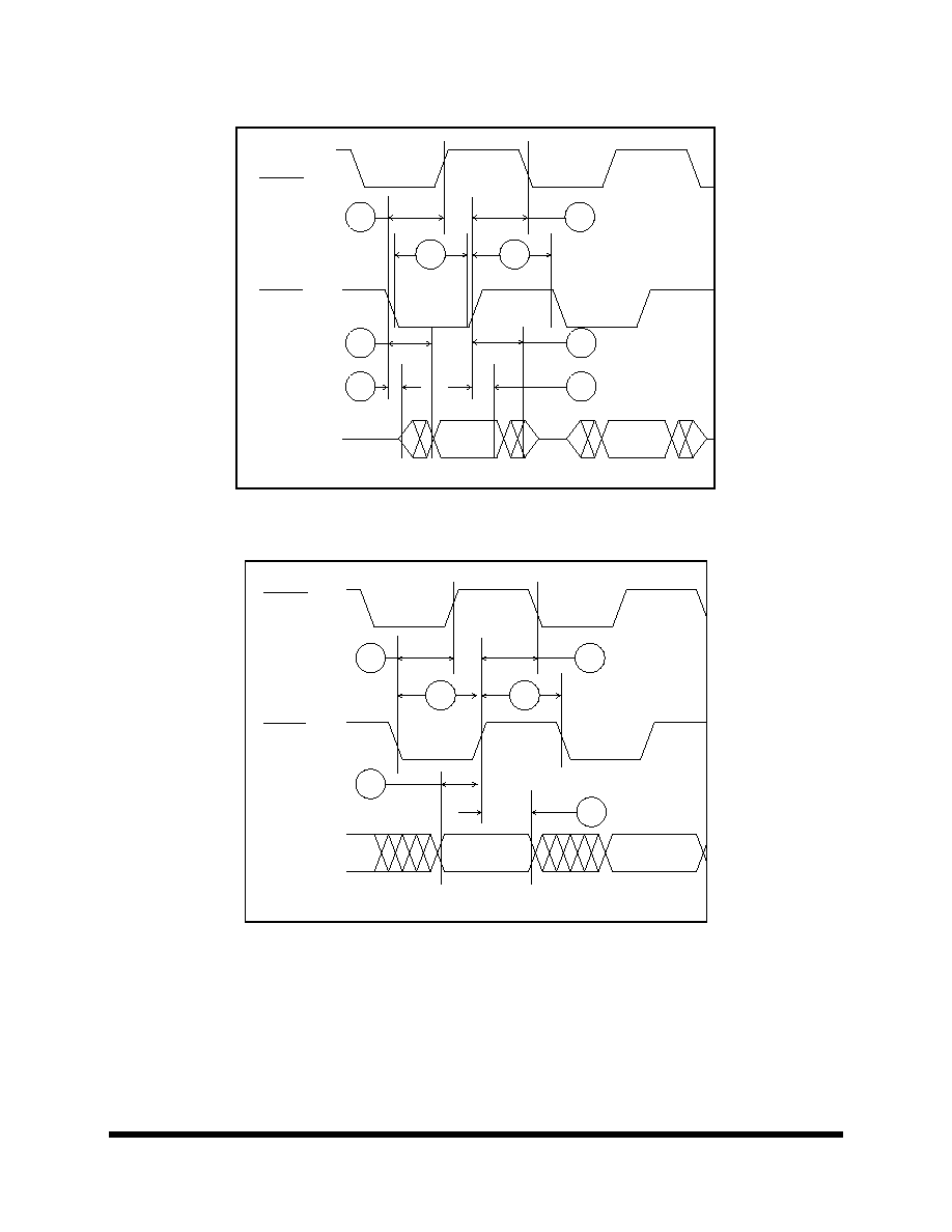
PRELIMINARY - 6/15/93
39
DSP56166 Technical Data Sheet
MOTOROLA
Host Figure 5. Host DMA Read Cycle
Host Figure 6. Host DMA Write Cycle
Data
Valid
Data
Valid
RXL
Read
RXH
Read
HREQ
(OUTPUT)
HACK
(INPUT)
H0-H7
(OUTPUT)
101
102
116
117
107
106
108
109
HREQ
(OUTPUT)
HACK
(INPUT)
H0-H7
(INPUT)
101
102
116
117
104
105
Data
Valid
Data
Valid
TXL
Write
TXH
Write
PRELIMINARY - 6/15/93
MOTOROLA
DSP56166 Technical Data Sheet
40
AC Electrical Characteristics -- RSSI Timing
(VCC = 5.0 Vdc +/- 10%, TJ = -40
∞
to + 125
∞
C, CL = 50 pF + 1 TTL Load, see RSSI Figure 1 and 2)
T = Icyc / 4
SCK Pin = Serial Clock
SFS Pin = Transmit/Receive Frame Sync
i ck = Internal Clock and Frame Sync
x ck = External Clock and Frame Sync
bl = bit length
wl = word length
NOTE:
All the timings for the RSSI are given for a non-inverted serial clock polarity (SCKP=0 in CRB) and a non-
inverted frame sync (FSI=0 in CRB). If the polarity of the clock and/or the frame sync have been inverted,
all the timings remain valid by inverting the clock signal SCK and/or the frame sync SFS in the tables and
in the figures.
Num
Characteristic
60MHz
Case
Unit
Min
Max
130
SCK Clock Cycle (see Note 1)
TBD
--
i ck
ns
131
SCK Clock High Period
TBD
--
i ck
ns
132
SCK Clock Low Period
TBD
--
i ck
ns
133
SCK Clock Rise/Fall Time
--
TBD
i ck
ns
134
SCK Rising Edge to SFS In (bl)
High
--
TBD
i ck
ns
135
SCK Rising Edge to SFS In (bl)
Low
--
TBD
i ck
ns
136
SCK Rising Edge to SFS In
(wl) High
--
TBD
i ck
ns
137
SCK Rising Edge to SFS In
(wl) Low
--
TBD
i ck
ns
138
Data In Setup Time Before
SCK Falling Edge
TBD
--
i ck
ns
139
Data In Hold Time After SCK
Falling Edge
TBD
--
i ck
ns

PRELIMINARY - 6/15/93
41
DSP56166 Technical Data Sheet
MOTOROLA
NOTES:
1. For internal clock, Serial Clock Cycle is defined by Icyc and RSSI control register.
Num
Characteristic
60MHz
Case
Unit
Min
Max
140
SCK Rising Edge to SFS Out (bl)
High
--
TBD
i ck
ns
141
SCK Rising Edge to SFS Out
(wl) High
--
TBD
i ck
ns
142
SCK Rising Edge to SFS Out
Low
--
TBD
i ck
ns
143
SCK Rising Edge to Data Out
Enable from High Impedance
--
TBD
i ck
ns
144
SCK Rising Edge to Data Out
Valid
--
TBD
i ck
ns
145
SCK Rising Edge to Data Out
Invalid
--
TBD
i ck
ns
146
SCK Rising Edge to Data Out
High Impedance
--
TBD
i ck
ns
AC Electrical Characteristics -- RSSI Timing (Continued)
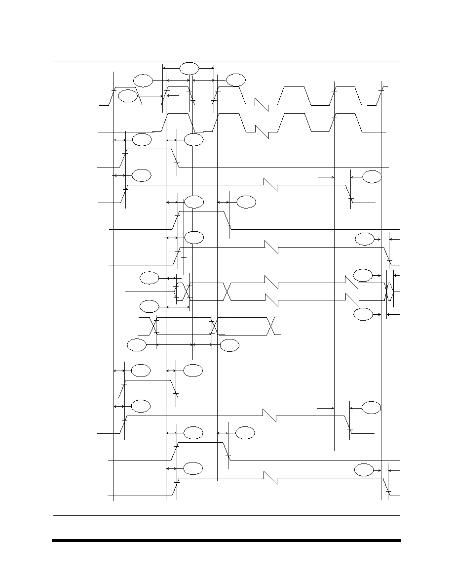
PRELIMINARY - 6/15/93
MOTOROLA
DSP56166 Technical Data Sheet
42
RSSI Figure 1. RSSI Internal ClockTiming
SCK Continuous
(Output)
SCK Gated
(Output)
SFS(Bit Early)
(Input)
SFS (Word Early)
(Input)
SFS(Bit )
(Input)
SFS (Word )
(Input)
STD (Output)
SRD (Input)
SFS(Bit Early)
(Output)
SFS (Word Early)
(Output)
SFS(Bit )
(Output)
SFS (Word )
(Output)
131
132
133
130
134
139
136
134
135
136
137
143
144
146
145
140
142
141
142
140
142
141
142
135
138
137
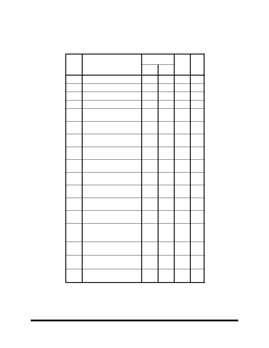
PRELIMINARY - 6/15/93
43
DSP56166 Technical Data Sheet
MOTOROLA
Num
Characteristic
60MHz
Case
Unit
Min
Max
150
SCK Clock Cycle (see Note 1)
TBD
--
x ck
ns
151
SCK Clock High Period
TBD
--
x ck
ns
152
SCK Clock Low Period
TBD
--
x ck
ns
153
SCK Clock Rise/Fall Time
--
TBD
x ck
ns
154
SCK Rising Edge to SFS Out
(bl) High
--
TBD
x ck
ns
155
SCK Rising Edge to SFS Out
(bl) Low
--
TBD
x ck
ns
156
SCK Rising Edge to SFS Out
(wl) High
--
TBD
x ck
ns
157
SCK Rising Edge to SFS Out
(wl) Low
--
TBD
x ck
ns
158
Data In Setup Time Before
SCK Falling Edge
TBD
--
x ck
ns
159
Data In Hold Time After SCK
Falling Edge
TBD
--
x ck
ns
160
SCK Rising Edge to SFS In (bl)
High
--
TBD
x ck
ns
161
SCK Rising Edge to SFS In (bl)
Low
--
TBD
x ck
ns
162
SCK Rising Edge to SFS In
(wl) High
--
TBD
x ck
ns
163
SCK Rising Edge to Data
Out Enable from High
Impedance
--
TBD
x ck
ns
164
SCK Rising Edge to Data
Out Valid
--
TBD
x ck
ns
165
SCK Rising Edge to Data
Out Invalid
--
TBD
x ck
ns
166
SCK Rising Edge to Data
Out High Impedance
--
TBD
x ck
ns
AC Electrical Characteristics -- RSSI Timing (Continued)

PRELIMINARY - 6/15/93
MOTOROLA
DSP56166 Technical Data Sheet
44
RSSI Figure 2. RSSI External ClockTiming
SCK Continuous
(Input)
SCK Gated
(Input)
SFS(Bit Early)
(Output)
SFS (Word Early)
(Output)
SFS(Bit )
(Output)
SFS (Word )
(Output)
STD (Output)
SRD (Input)
SFS(Bit Early)
(Input)
SFS (Word Early)
(Input)
SFS(Bit )
(Input)
SFS (Word )
(Input)
151
152
153
150
154
159
156
154
155
156
157
163
164
166
165
160
162
161
162
160
162
161
162
155
158
157

PRELIMINARY - 6/15/93
45
DSP56166 Technical Data Sheet
MOTOROLA
AC Electrical Characteristics -- Timer Timing
(VCC = 5.0 Vdc +/- 10%, TJ = -40 to +125
∞
C, CL = 50 pF + 1 TTL Load).
Timer Figure 1. Timer Timing
Num
Characteristic
60MHz
Unit
Min
Max
170
TIN Valid to CLKO low (Setup time)
6
--
ns
171
CLKO Low to TIN Invalid (Hold time)
0
--
ns
172
CLKO High to TOUT Asserted
3.5
14
ns
173
CLKO High to TOUT Deasserted
5.1
20.7
ns
174
Tin Period
8T
--
ns
175
Tin High/Low Period
4T
--
ns
173
170
172
171
CLKO
(Output)
TIN
(Input)
TOUT
(Output)
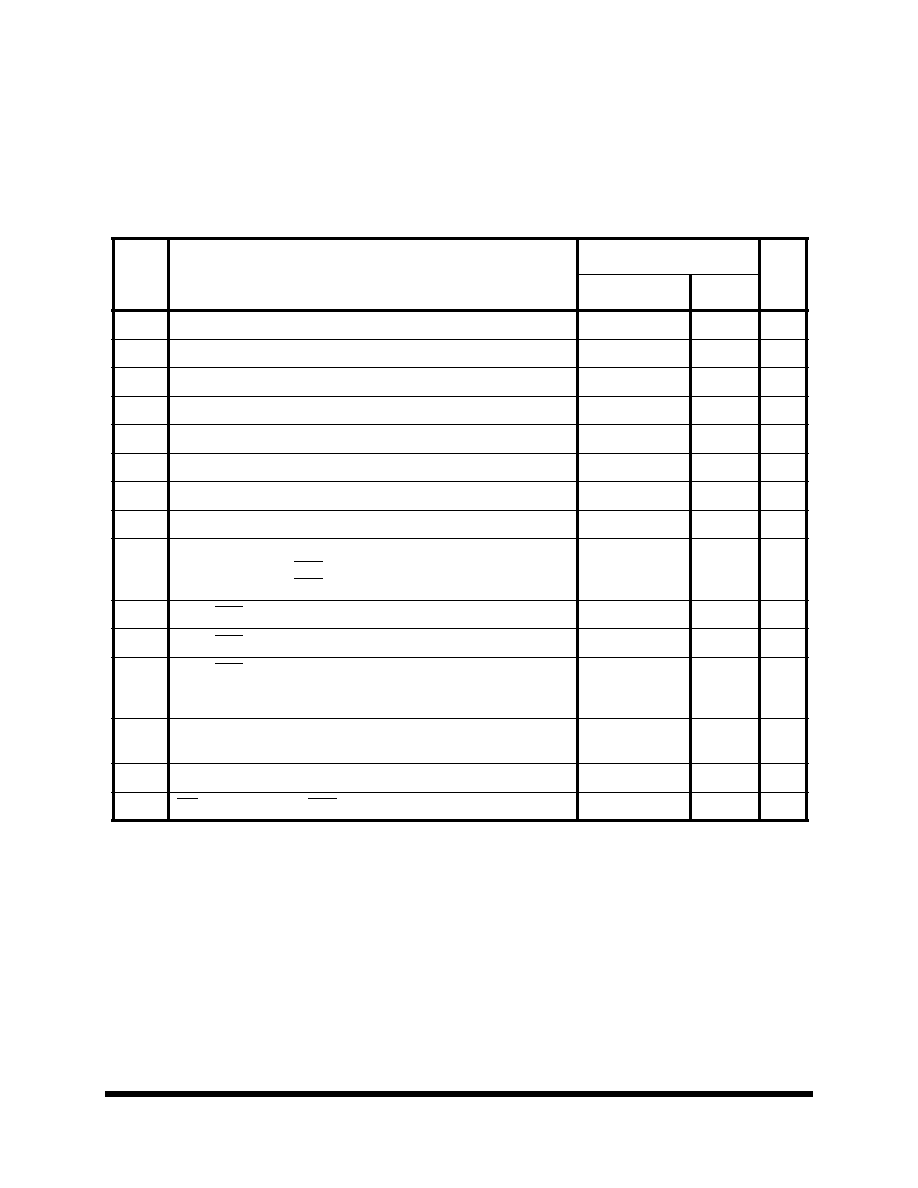
PRELIMINARY - 6/15/93
MOTOROLA
DSP56166 Technical Data Sheet
46
AC Electrical Characteristics -- OnCE Timing
VCC = 5.0 Vdc +/- 10%, TJ = -40
∞
to +125
∞
C, CL = 50 pF + 1 TTL Load).
NOTES:
1. 45%-55% duty cycle
2. Td=DSCK High (183)
Num
Characteristic
60 MHz
Unit
Min
Max
180
DSCK High to DSO Valid
--
27.6
ns
181
DSI Valid to DSCK Low (Setup)
1
--
ns
182
DSCK Low to DSI Invalid (Hold)
0.9
--
ns
183
DSCK High (See note 1)
2Tc
--
ns
184
DSCK Low (See note 1)
2Tc
--
ns
185
DSCK Cycle Time (See note 1)
4Tc
--
ns
186
CLKO High to OS0-OS1 Valid
14.5
ns
187
CLKO High to OS0-OS1 Invalid
--
--
ns
188
Last DSCK High to OS0-OS1(See note 2)
Last DSCK High to ACK Active (data)(See note 2)
Last DSCK High to ACK Active (command)(See note 2)
10T+Td+14.5
10T+Td+13.5
21T+Td+13.5
--
--
ns
189
DSO (ACK) Asserted to OS0-OS1 Three-state
--
TBD
ns
190
DSO (ACK) Asserted to First DSCK High
3Tc
--
ns
191
DSO (ACK) Width Asserted:
a. when entering debug mode
b. when acknowledging command/data transfer
8T+1.1
9T+1.1
8T+4.1
9T+4.1
ns
ns
192
Last DSCK Low of Read Register to First
DSCK High of Next Command
6Tc
--
ns
193
DSCK High to DSO Invalid (See note 2)
10.9
--
ns
194
DR asserted to DSO (ACK) Asserted
11T+19.5
--
ns

PRELIMINARY - 6/15/93
47
DSP56166 Technical Data Sheet
MOTOROLA
OnCE Figure 1. OnCE Serial Clock Timing
OnCE Figure 2. OnCE Acknowledge Timing
OnCE Figure 3. OnCE Data I/O To Status Timing
DSCK
(Input)
185
183
184
194
ACK
DR
(Input)
DSO
(Output)
188
(ACK)
(OS0)
(OS1)
(Last)
DSCK
(Input)
DSO
(Output)
DSI
(Input)
193
180
181
182
Note 1
Note 1: Three-state, external pull-down resistor

PRELIMINARY - 6/15/93
MOTOROLA
DSP56166 Technical Data Sheet
48
OnCE Figure 4. OnCE Data I/O To Status Timing
OnCE Figure 5. OnCE CLK To Status Timing
OnCE Figure 6. OnCE DSCK Next Command After Read Register Timing
191
190
180
(Note 1)
Note 1: Three-state, external pull-down resistor
OS1
(Output)
DSO
(Output)
OS0
(Output)
(DSCK input)
182
181
189
(DSO Output)
(DSI input)
CLKO
(Output)
OS0-1
(Output)
187
186
192
(Read Register)
(Next Command)
DSCK
(Input)

PRELIMINARY - 6/15/93
49
DSP56166 Technical Data Sheet
MOTOROLA
AC Electrical Characteristics -- General Purpose I/O (GPIO) Timing
(VCC = 5.0 Vdc +/- 10%, TJ = -40 to +125
∞
C, CL = 50 pF + 1 TTL Load).
GPIO Figure 1. GPIO Timing
Num
Characteristic
60 MHz
Unit
Min
Max
201
CLKO Edge to GPIO Out Valid
(GPIO Out Delay Time)
TBD
TBD
ns
202
CLKO Edge to GPIO Out Not Valid
(GPIO Out Hold Time)
TBD
TBD
ns
203
GPIO In Valid to CLKO Edge
(GPIO In Set-upTime)
TBD
TBD
ns
204
CLKO Edge to GPIO In Not Valid
(GPIO In Hold Time)
TBD
TBD
ns
204
CLKO
(Output)
GPIO
(Output)
GPIO
(Input)
201
202
203
VALID

MOTOROLA
TECHNICAL DATA
SEMICONDUCTOR
MOTOROLA
The DSP56166ROM is the second member of Motorola's DSP56100 family of HCMOS, low power, 16-bit general purpose Digital
Signal Processors (DSP). Designed primarily for speech coding and digital communications, the DSP56166ROM has a built-in
codec and phase locked loop (PLL). This MPU-style DSP also contains, memories, peripherals, and provides a cost effective, high
performance solution to many DSP applications. On-Chip Emulation (OnCE
TM
) circuitry provides convenient and inexpensive debug
facilities normally available only through expensive external hardware. Development costs are reduced and in-field testing is greatly
simplified by using the OnCE. The DSP56166 ROM based part contains a 12K ROM (8K x 16 program ROM and 4K x 16 data ROM).
The Central Processing Unit (CPU) consists of three execution units operating in parallel allowing up to six operations to occur in an
instruction cycle. This parallelism greatly increases the effective processing speed of the DSP56166ROM. The MPU-style program-
ming model and instruction set allow straightforward generation of efficient, compact code. The basic architectures and development
tools of the DSP56100, DSP56000, and DSP96000 families are so similar that learning to design and program one greatly reduces
the time needed to learn the others.
Advance Information
16-bit General Purpose
Digital Signal Processor
DSP56166ROM
Ceramic Quad Flat Pack (CQFP)
Available in a 112 pin, small footprint,
surface mount package.
∑ Up to 30 Million Instructions per Second (MIPS) at 60
MHz.≠ 33.3 ns Instruction cycle
∑ Single-cycle 16 x 16-bit parallel Multiply-Accumulate
∑ 2 x 40-bit accumulators with extension byte
∑ Fractional and integer arithmetic with support for
multiprecision arithmetic
∑ Highly parallel instruction set with unique DSP
addressing modes
∑ Nested hardware DO loops including infinite loops and
DO zero loop
∑ Two instruction LMS adaptive filter loop
∑ Fast auto-return interrupts
∑ Three external interrupt request pins
∑ Three 16-bit internal data and three 16-bit internal
address buses
∑ Individual programmable wait states on the external bus
for program, data, and peripheral memory spaces
∑ Off-chip memory-mapped peripheral space with
programmable access time and separate peripheral
enable pin
∑ On-chip memory-mapped peripheral registers
∑ Low Power Wait and Stop modes
∑ On-Chip Emulation (OnCE
)
for unobtrusive, processor
speed independent debugging
∑ Operating frequency down to DC
∑ 5V single power supply
∑ Low power (HCMOS)
∑ 4K x 16 on-chip data RAM
∑ 4K x 16 on-chip data ROM
∑ 256 x 16 on-chip program RAM
∑ 8K x 16 on-chip program ROM
∑ One external 16-bit address bus
∑ One external 16-bit data bus
∑ On-chip
voice band codec (A/D-D/A)
≠ Internal voltage reference (2/5 of positive power
supply)
≠ No off-chip components required
∑ 25 general purpose I/O pins
∑ On-chip, programmable PLL
∑ Byte-wide Host Interface with DMA support
∑ Two independent reduced synchronous serial
interfaces
∑ One 16-bit timer
∑ 112 pin quad flat pack packaging
∑ XROM can only be accessed during a single read or the
first read of a dual parallel read instruction (see note on
back.
∑ No bootstrap ROM
∑ Reset mode 1 vectors to P:$0100
∑ PROM area P:$2080 -- P:$20FF is reserved and
should not be programmed or accessed by the user
DSP56166ROM Feature List
DSP56166ROM On-chip Resources
Operational Differences Of The ROM Based Part From The RAM Based Part
DSP56100 Family Features
This document contains information on a new product. Specifications and information herein are subject to change without notice.
Order this document
by DSP56166ROM/D
©
MOTOROLA INC., 1993
July 14, 1993

Literature Distribution Centers
USA:
Motorola Literature Distribution; P.O. Box 20912; Phoenix, Arizona 85036.
EUROPE: Motorola Ltd.; European Literature Centre; 88 Tanners Drive, Blakelands, Milton Keynes, MK14 5BP, United Kingdom.
JAPAN:
Nippon Motorola Ltd.; 4-32-1, Nishi-Gotanda, Shinagawa-ku, Tokyo 141 Japan.
ASIA-PACIFIC: Motorola Semiconductors H.K. Ltd.; Silicon Harbor Center, No. 2 Dai King Street, Tai Po Industrial
Estate, Tai Po, N.T., Hong Kong.
Motorola reserves the right to make changes without further notice to any products herein. Motorola makes no warranty, repre-
sentation or guarantee regarding the suitability of its products for any particular purpose, nor does Motorola assume any liability
arising out of the application or use of any product or circuit, and specifically disclaims any and all liability, including without limi-
tation consequential or incidental damages. "Typical" parameters can and do vary in different applications. All operating param-
eters, including "Typical", must be validated for each customer application by customer's technical experts. Motorola does not
convey any license under its patent rights nor the rights of others. Motorola products are not designed, intended, or authorized
for use as components in systems intended for surgical implant into the body, or other applications intended to support or sustain
life, or for any other application in which the failure of the Motorola product could create a situation where personal injury or death
may occur. Should Buyer purchase or use Motorola products for any such unintended or unauthorized application, Buyer shall
indemnify and hold Motorola and its officers, employees, subsidiaries, affiliates, and distributors harmless against all claims,
costs, damages, and expenses, and reasonable attorney fees arising out of, directly or indirectly, any claim of personal injury or
death associated with such unintended or unauthorized use, even if such claim alleges that Motorola was negligent regarding the
design or manufacture of the part.
Motorola and
b
are registered trademarks of Motorola, Inc.
Motorola, Inc. is an Equal Opportunity/Affirmative Action Employer.
OnCE is a trademark of Motorola, Inc.
All product and brand names appearing herein are trademarks or registered trademarks of their respective holders.

MOTOROLA
DSP56166ROM Block Diagram
Note
: Since the on-chip XROM is only connected to the XAB1 address bus (see the block diagram above), the data located in this
ROM is only accessible by the
first
read of a single read instruction or the
first
read of a dual parallel read instruction.
Therefore, during development using the RAM based part, the data to be mapped in the on-chip XROM on the ROM based
part
should not
be accessed with a
second
read during a dual parallel read instruction.
XDB
PDB
GDB
4
7+10
ADDRESS
POR
T A
PROGRAM CONTROL UNIT
MODA/IRQA
MODB/IRQB
ON-CHIP
PERIPHERALS
HOST, RSSI0,
RSSI1, TIMER
GPI/O, CODEC
INTERNAL DATA
BUS SWITCH
AND BIT
MANIPULATION
UNIT
EXTERNAL
ADDRESS
BUS
SWITCH
BUS
CONTROL
EXTERNAL
DATA BUS
SWITCH
PRAM
256 x 16
PROGRAM
ADDRESS
GENERATOR
PROGRAM
DECODE
CONTROLLER
PROGRAM
INTERRUPT
CONTROLLER
DATA ALU
16x16+40 - 40-BIT MAC
TWO 40-BIT ACCUMULATORS
CLOCK
AND PLL
EXTAL
PORT B
OR
HOST
15
CODEC,
PORT C
AND/OR
RSSI0,
RSSI1,
TIMER
RESET
16 BITS
DATA
10
OnCE
SXFC
CLKO
XAB1
XAB2
PAB
ADDRESS
GENERATION
UNIT
16
16
MODC/IRQC
PROM
8K x 16
DATA
RAM
4Kx16
DATA
ROM
4Kx16
PROGRAM
DATA MEMORY
MEMORY
In the USA:
For technical assistance call:
DSP Applications Helpline (512) 891-3230
For availability and literature call your local Motorola Sales Office or Authorized Distributor.
For free application software and information call the Dr. BuB electronic bulletin board:
9600/4800/2400/1200/300 baud
(512) 891-3771
(8 data bits, no parity, 1 stop)
In Europe, Japan and Asia Pacific
Contact your regional sales office or Motorola distributor.
Literature Distribution Centers:
USA: Motorola Literature Distribution; P.O. Box 20912; Phoenix, Arizona 85036.
EUROPE: Motorola Ltd.; European Literature Center; 88 Tanners Drive, Blakelands, Milton Keynes, MK14 5BP, England.
JAPAN: Nippon Motorola Ltd.; 4-32-1, Nishi-Gotanda, Shinagawa-ku, Tokyo 141 Japan.
ASIA-PACIFIC: Motorola Semiconductors H.K. Ltd.; Silicon Harbor Center, No. 2 Dai King Street, Tai Po Industrial Estate, Tai Po, N.T.,
Hong Kong.
Motorola reserves the right to make changes without further notice to any products herein. Motorola makes no warranty, representation or guarantee regarding
the suitability of its products for any particular purpose, nor does Motorola assume any liability arising out of the application or use of any product or circuit, and
specifically disclaims any and all liability, including without limitation consequential or incidental damages. "Typical" parameters can and do vary in different
applications. All operating parameters, including "Typicals" must be validated for each customer application by customer's technical experts. Motorola does not
convey any license under its patent rights nor the rights of others. Motorola products are not designed, intended, or authorized for use as components in systems
intended for surgical implant into the body, or other applications intended to support or sustain life, or for any other application in which the failure of the Motorola
product could create a situation where personal injury or death may occur. Should Buyer purchase or use Motorola products for any such unintended or unau-
thorized application, Buyer shall indemnify and hold Motorola and its officers, employees, subsidiaries, affiliates, and distributors harmless against all claims,
costs, damages, and expenses, and reasonable attorney fees arising out of, directly or indirectly, any claim of personal injury or death associated with such
unintended or unauthorized use, even if such claim alleges that Motorola was negligent regarding the design or manufacture of the part. Motorola and M are
registered trademarks of Motorola, Inc. Motorola, Inc. is an Equal Opportunity/Affirmative Action Employer.

Corrections to the DSP56166 Data Sheet Dated 6/15/93
1. Remove the entry for the BIAS pin (page 9 of the 6/15/93 data sheet)