
HC05
MC68HC05X16/D
Rev. 1
MC68HC05X16
MC68HC05X32
MC68HC705X32
TECHNICAL
DATA
MC68HC05X16
TECHNICAL DATA

1
2
3
4
5
6
7
8
9
10
11
12
13
14
15
1
INTRODUCTION
MODES OF OPERATION AND PIN DESCRIPTIONS
MEMORY AND REGISTERS
INPUT/OUTPUT PORTS
MOTOROLA CAN MODULE (MCAN)
PROGRAMMABLE TIMER
SERIAL COMMUNICATIONS INTERFACE
PULSE LENGTH D/A CONVERTERS
ANALOG TO DIGITAL CONVERTER
RESETS AND INTERRUPTS
CPU CORE AND INSTRUCTION SET
ELECTRICAL SPECIFICATIONS
MECHANICAL DATA
ORDERING INFORMATION
APPENDICES

1
2
3
4
5
6
7
8
9
10
11
12
13
14
15
INTRODUCTION
MODES OF OPERATION AND PIN DESCRIPTIONS
MEMORY AND REGISTERS
INPUT/OUTPUT PORTS
MOTOROLA CAN MODULE (MCAN)
PROGRAMMABLE TIMER
SERIAL COMMUNICATIONS INTERFACE
PULSE LENGTH D/A CONVERTERS
ANALOG TO DIGITAL CONVERTER
RESETS AND INTERRUPTS
CPU CORE AND INSTRUCTION SET
ELECTRICAL SPECIFICATIONS
MECHANICAL DATA
ORDERING INFORMATION
APPENDICES
2

All products are sold on Motorola's Terms & Conditions of Supply. In ordering a product covered by this document the
Customer agrees to be bound by those Terms & Conditions and nothing contained in this document constitutes or forms part
of a contract (with the exception of the contents of this Notice). A copy of Motorola's Terms & Conditions of Supply is available
on request.
Motorola reserves the right to make changes without further notice to any products herein. Motorola makes no warranty,
representation or guarantee regarding the suitability of its products for any particular purpose, nor does Motorola assume any
liability arising out of the application or use of any product or circuit, and specifically disclaims any and all liability, including
without limitation consequential or incidental damages. "Typical" parameters can and do vary in different applications. All
operating parameters, including "Typicals", must be validated for each customer application by customer's technical experts.
Motorola does not convey any license under its patent rights nor the rights of others. Motorola products are not designed,
intended, or authorized for use as components in systems intended for surgical implant into the body, or other applications
intended to support or sustain life, or for any other application in which the failure of the Motorola product could create a
situation where personal injury or death may occur. Should Buyer purchase or use Motorola products for any such unintended
or unauthorized application, Buyer shall indemnify and hold Motorola and its officers, employees, subsidiaries, affiliates, and
distributors harmless against all claims, costs, damages, and expenses, and reasonable attorney fees arising out of, directly
or indirectly, any claim of personal injury or death associated with such unintended or unauthorized use, even if such claim
alleges that Motorola was negligent regarding the design or manufacture of the part. Motorola and
are registered
trademarks of Motorola, Inc. Motorola, Inc. is an Equal Opportunity/Affirmative Action Employer.
The Customer should ensure that it has the most up to date version of the document by contacting its local Motorola office.
This document supersedes any earlier documentation relating to the products referred to herein. The information contained
in this document is current at the date of publication. It may subsequently be updated, revised or withdrawn.
©
MOTOROLA LTD., 1997
All Trade Marks recognized. This document contains information on new products. Specifications and information herein are
subject to change without notice.
MC68HC05X16
MC68HC05X32
MC68HC705X32
High-density complementary
metal oxide semiconductor
(HCMOS) microcontroller unit
3

4
Conventions
Where abbreviations are used in the text, an explanation can be found in the
glossary, at the back of this manual. Register and bit mnemonics are defined in the
paragraphs describing them.
An overbar is used to designate an active-low signal, eg: RESET.
Unless otherwise stated, a shaded cell in a register diagram indicates that the bit is
either unused or reserved; `u' is used to indicate an undefined state (on reset).
Unless otherwise stated, a pin labelled as `NU' should be tied to V
SS
in an electrically
noisy environment. Pins labelled `NC' can be left floating, since they are not bonded
to any part of the device.

CUSTOMER FEEDBACK QUESTIONNAIRE (MC68HC05X16/D)
Motorola wishes to continue to improve the quality of its documentation. We would welcome your feedback on the publication you
have just received. Having used the document, please complete this card (or a photocopy of it, if you prefer).
1.
How would you rate the quality of the document? Check one box in each category.
Excellent
Poor
Excellent
Poor
Organization
t t t t
Tables
t t t t
Readability
t t t t
Table of contents
t t t t
Understandability
t t t t
Index
t t t t
Accuracy
t t t t
Page size/binding
t t t t
Illustrations
t t t t
Overall impression
t t t t
Comments:
2.
What is your intended use for this document? If more than one option applies, please rank them (1, 2, 3).
Selection of device for new application
t
Other
t
Please specify:
System design
t
Training purposes
t
3.
How well does this manual enable you to perform the task(s) outlined in question 2?
Completely
Not at all
Comments:
t t t t
4.
How easy is it to find the information you are looking for?
Easy
Difficult
Comments:
t t t t
5.
Is the level of technical detail in the following sections sufficient to allow you to understand how the device functions?
Too little detail
Too much detail
t t t t t
t t t t t
t t t t t
t t t t t
t t t t t
t t t t t
t t t t t
t t t t t
t t t t t
t t t t t
t t t t t
t t t t t
t t t t t
t t t t t
t t t t t
Comments:
6.
Have you found any errors? If so, please comment:
7.
From your point of view, is anything missing from the document? If so, please say what:
≠ Cut along this line to remo
v
e
≠
¢
SECTION 1
INTRODUCTION
SECTION 2
MODES OF OPERATION AND PIN DESCRIPTIONS
SECTION 3
MEMORY AND REGISTERS
SECTION 4
INPUT/OUTPUT PORTS
SECTION 5
MOTOROLA CAN MODULE (MCAN)
SECTION 6
PROGRAMMABLE TIMER
SECTION 7
SERIAL COMMUNICATIONS INTERFACE
SECTION 8
PULSE LENGTH D/A CONVERTERS
SECTION 9
ANALOG TO DIGITAL CONVERTER
SECTION 10
RESETS AND INTERRUPTS
SECTION 11
CPU CORE AND INSTRUCTION SET
SECTION 12
ELECTRICAL SPECIFICATIONS
SECTION 13
MECHANICAL DATA
SECTION 14
ORDERING INFORMATION
SECTION 15
APPENDICES
5

13. Currently there is some discussion in the semiconductor industry regarding a move towards providing data sheets in electronic
form. If you have any opinion on this subject, please comment.
14. We would be grateful if you would supply the following information (at your discretion), or attach your card.
Name:
Phone No:
Position:
FAX No:
Department:
Company:
Address:
Thank you for helping us improve our documentation,
Graham Forbes, Technical Publications Manager, Motorola Ltd., Scotland
.
≠ Cut along this line to remo
v
e
≠
≠ Third fold back along this line ≠
8.
How could we improve this document?
9.
How would you rate Motorola's documentation?
Excellent
Poor
≠ In general
t t t t
≠ Against other semiconductor suppliers
t t t t
10. Which semiconductor manufacturer provides the best technical documentation?
11. Which company (in any field) provides the best technical documentation?
12. How many years have you worked with microprocessors?
Less than 1 year
t
1≠3
years
t
3≠5 years
t
More than 5 years
t
By air mail
Par avion
NE PAS AFFRANCHIR
IBRS NUMBER PHQ-B/207/G
CCRI NUMERO PHQ-B/207/G
REPONSE PAYEE
GRANDE-BRETAGNE
Motorola Ltd.,
Colvilles Road,
Kelvin Industrial Estate,
EAST KILBRIDE,
G75 8BR.
GREAT BRITAIN.
F.A.O. Technical Publications Manager
(re: MC68HC05X16/D)
NO STAMP REQUIRED
≠ First f
old bac
k along this line ≠
Semiconductor Products Sector
≠ Second fold back along this line ≠
≠ Finally, tuck this edge into opposite flap ≠
¢
6

MC68HC05X16
Rev. 1
MOTOROLA
i
TABLE OF CONTENTS
Paragraph
Number
Page
Number
TITLE
TABLE OF CONTENTS
1
INTRODUCTION
1.1
Features ................................................................................................................ 1-2
1.2
Mask options for the MC68HC05X16 .................................................................... 1-3
2
MODES OF OPERATION AND
PIN DESCRIPTIONS
2.1
Modes of operation................................................................................................ 2-1
2.1.1
Single-chip mode ............................................................................................. 2-1
2.1.2
Bootstrap mode ............................................................................................... 2-2
2.1.2.1
Serial RAM loader ...................................................................................... 2-3
2.1.2.2
Jump to RAM + 1 ....................................................................................... 2-3
2.1.2.3
`Jump to any address' ................................................................................ 2-3
2.2
Low power modes ................................................................................................. 2-6
2.2.1
STOP mode ..................................................................................................... 2-6
2.2.2
WAIT mode ...................................................................................................... 2-7
2.2.2.1
Power consumption during WAIT mode ..................................................... 2-8
2.2.3
SLOW mode .................................................................................................... 2-8
2.2.3.1
Miscellaneous register .............................................................................. 2-10
2.3
Pin descriptions ..................................................................................................... 2-11
2.3.1
VDD and VSS .................................................................................................. 2-11
2.3.2
IRQ .................................................................................................................. 2-11
2.3.3
RESET ............................................................................................................. 2-11
2.3.4
MDS ................................................................................................................. 2-12
2.3.5
TCAP1 ............................................................................................................. 2-12
2.3.6
TCAP2 ............................................................................................................. 2-12
2.3.7
TCMP1............................................................................................................. 2-12
2.3.8
TCMP2............................................................................................................. 2-12
2.3.9
RDI (Receive data in)....................................................................................... 2-12
2.3.10
TDO (Transmit data out) .................................................................................. 2-12
2.3.11
SCLK ............................................................................................................... 2-13
7

MOTOROLA
ii
MC68HC05X16
Rev. 1
TABLE OF CONTENTS
Paragraph
Number
Page
Number
TITLE
2.3.12
OSC1, OSC2 ................................................................................................... 2-13
2.3.12.1
Crystal........................................................................................................ 2-13
2.3.12.2
Ceramic resonator ..................................................................................... 2-13
2.3.12.3
External clock............................................................................................. 2-13
2.3.12.4
Oscillator division ....................................................................................... 2-15
2.3.13
PLMA ............................................................................................................... 2-15
2.3.14
PLMB ............................................................................................................... 2-15
2.3.15
VPP1 ............................................................................................................... 2-16
2.3.16
VRH ................................................................................................................. 2-16
2.3.17
VRL.................................................................................................................. 2-16
2.3.18
PA0 ≠ PA7/PB0 ≠ PB7/PC0 ≠ PC7 .................................................................. 2-16
2.3.19
NWOI ............................................................................................................... 2-16
2.3.20
PD0/AN0≠PD7/AN7......................................................................................... 2-16
2.3.21
VDD1 ............................................................................................................... 2-17
2.3.22
VSS1 ............................................................................................................... 2-17
2.3.23
VDDH .............................................................................................................. 2-17
2.3.24
RX0/RX1.......................................................................................................... 2-17
2.3.25
TX0/TX1 .......................................................................................................... 2-17
3
MEMORY AND REGISTERS
3.1
Registers ............................................................................................................... 3-1
3.2
RAM ...................................................................................................................... 3-1
3.3
ROM ...................................................................................................................... 3-1
3.4
Bootstrap ROM...................................................................................................... 3-3
3.5
EEPROM............................................................................................................... 3-4
3.5.1
EEPROM control register ................................................................................ 3-4
3.5.2
EEPROM read operation ................................................................................. 3-6
3.5.3
EEPROM erase operation ............................................................................... 3-6
3.5.4
EEPROM programming operation ................................................................... 3-7
3.5.5
Options register (OPTR) .................................................................................. 3-7
3.6
EEPROM during STOP mode ............................................................................... 3-8
3.7
EEPROM during WAIT mode ................................................................................ 3-8
3.8
Miscellaneous register.......................................................................................... 3-11
4
INPUT/OUTPUT PORTS
4.1
Input/output programming ..................................................................................... 4-1
4.2
Ports A and B ........................................................................................................ 4-2
4.3
Port C .................................................................................................................... 4-3
4.4
Port D .................................................................................................................... 4-4
4.5
Port registers ......................................................................................................... 4-4
8

MC68HC05X16
Rev. 1
MOTOROLA
iii
TABLE OF CONTENTS
Paragraph
Number
Page
Number
TITLE
4.5.1
Port data registers A and B (PORTA and PORTB) .......................................... 4-4
4.5.2
Port data register C (PORTC).......................................................................... 4-5
4.5.3
Port data register D (PORTD).......................................................................... 4-5
4.5.4
A/D status/control register ............................................................................... 4-5
4.5.5
Data direction registers (DDRA, DDRB and DDRC)........................................ 4-6
4.6
Other port considerations ...................................................................................... 4-6
5
MOTOROLA CAN MODULE (MCAN)
5.1
TBF ≠ Transmit buffer ............................................................................................ 5-4
5.2
RBF ≠ Receive buffer ............................................................................................ 5-4
5.3
Interface to the MC68HC05X16 CPU .................................................................... 5-4
5.3.1
MCAN control register (CCNTRL) ................................................................... 5-6
5.3.2
MCAN command register (CCOM) .................................................................. 5-7
5.3.3
MCAN status register (CSTAT) ........................................................................ 5-10
5.3.4
MCAN interrupt register (CINT) ....................................................................... 5-12
5.3.5
MCAN acceptance code register (CACC)........................................................ 5-13
5.3.6
MCAN acceptance mask register (CACM) ...................................................... 5-14
5.3.7
MCAN bus timing register 0 (CBT0) ................................................................ 5-14
5.3.8
MCAN bus timing register 1 (CBT1) ................................................................ 5-16
5.3.9
MCAN output control register (COCNTRL)...................................................... 5-18
5.3.10
Transmit buffer identifier register (TBI)............................................................. 5-20
5.3.11
Remote transmission request and data length code register (TRTDL)............ 5-20
5.3.12
Transmit data segment registers (TDS) 1 ≠ 8 .................................................. 5-21
5.3.13
Receive buffer identifier register (RBI) ............................................................. 5-21
5.3.14
Remote transmission request and data length code register (RRTDL) ........... 5-22
5.3.15
Receive data segment registers (RDS) 1 ≠ 8 .................................................. 5-22
5.4
Interface to the MCAN bus .................................................................................... 5-22
5.4.1
Single wire operation ....................................................................................... 5-24
5.5
Sleep mode ........................................................................................................... 5-24
5.5.1
Sleep comparator reference ............................................................................ 5-25
6
PROGRAMMABLE TIMER
6.1
Counter.................................................................................................................. 6-1
6.1.1
Counter register and alternate counter register ............................................... 6-3
6.2
Timer control and status ........................................................................................ 6-4
6.2.1
Timer control register (TCR) ............................................................................ 6-4
6.2.2
Timer status register (TSR) ............................................................................. 6-6
6.3
Input capture.......................................................................................................... 6-7
6.3.1
Input capture register 1 (ICR1) ........................................................................ 6-7
6.3.2
Input capture register 2 (ICR2) ........................................................................ 6-8
9

MOTOROLA
iv
MC68HC05X16
Rev. 1
TABLE OF CONTENTS
Paragraph
Number
Page
Number
TITLE
6.4
Output compare..................................................................................................... 6-9
6.4.1
Output compare register 1 (OCR1) ................................................................. 6-9
6.4.2
Output compare register 2 (OCR2) ................................................................. 6-10
6.4.3
Software force compare................................................................................... 6-11
6.5
Pulse length modulation (PLM) ............................................................................. 6-11
6.5.1
Pulse length modulation registers A and B (PLMA/PLMB).............................. 6-11
6.6
Timer during STOP mode ..................................................................................... 6-12
6.7
Timer during WAIT mode ...................................................................................... 6-12
6.8
Timer state diagrams............................................................................................. 6-12
7
SERIAL COMMUNICATIONS INTERFACE
7.1
SCI two-wire system features................................................................................ 7-1
7.2
SCI receiver features............................................................................................. 7-3
7.3
SCI transmitter features......................................................................................... 7-3
7.4
Functional description ........................................................................................... 7-3
7.5
Data format............................................................................................................ 7-5
7.6
Receiver wake-up operation.................................................................................. 7-5
7.6.1
Idle line wake-up.............................................................................................. 7-6
7.6.2
Address mark wake-up .................................................................................... 7-6
7.7
Receive data in (RDI) ............................................................................................ 7-6
7.8
Start bit detection .................................................................................................. 7-6
7.9
Transmit data out (TDO) ........................................................................................ 7-8
7.10
SCI synchronous transmission.............................................................................. 7-9
7.11
SCI registers.......................................................................................................... 7-10
7.11.1
Serial communications data register (SCDR) .................................................. 7-10
7.11.2
Serial communications control register 1 (SCCR1) ......................................... 7-10
7.11.3
Serial communications control register 2 (SCCR2) ......................................... 7-14
7.11.4
Serial communications status register (SCSR) ............................................... 7-16
7.11.5
Baud rate register (BAUD) ............................................................................... 7-18
7.12
Baud rate selection................................................................................................ 7-20
7.13
SCI during STOP mode......................................................................................... 7-21
7.14
SCI during WAIT mode.......................................................................................... 7-21
8
PULSE LENGTH D/A CONVERTERS
8.1
Miscellaneous register........................................................................................... 8-3
8.2
PLM clock selection............................................................................................... 8-4
8.3
PLM during STOP mode ....................................................................................... 8-4
8.4
PLM during WAIT mode ........................................................................................ 8-4
10

MC68HC05X16
Rev. 1
MOTOROLA
v
TABLE OF CONTENTS
Paragraph
Number
Page
Number
TITLE
9
ANALOG TO DIGITAL CONVERTER
9.1
A/D converter operation......................................................................................... 9-1
9.2
A/D registers.......................................................................................................... 9-3
9.2.1
Port D data register (PORTD).......................................................................... 9-3
9.2.2
A/D result data register (ADDATA) ................................................................... 9-3
9.2.3
A/D status/control register (ADSTAT)............................................................... 9-4
9.3
A/D converter during STOP mode ......................................................................... 9-5
9.4
A/D converter during WAIT mode.......................................................................... 9-6
9.5
Port D analog input................................................................................................ 9-6
10
RESETS AND INTERRUPTS
10.1
Resets ................................................................................................................. 10-1
10.1.1
Power-on reset............................................................................................... 10-2
10.1.2
Miscellaneous register .................................................................................. 10-2
10.1.3
RESET pin ..................................................................................................... 10-3
10.1.4
Computer operating properly (COP) watchdog reset .................................... 10-3
10.1.4.1
COP watchdog during STOP mode ......................................................... 10-5
10.1.4.2
COP watchdog during WAIT mode .......................................................... 10-5
10.1.5
Functions affected by reset............................................................................ 10-5
10.2
Interrupts ............................................................................................................. 10-7
10.2.1
Interrupt priorities........................................................................................... 10-9
10.2.2
Nonmaskable software interrupt (SWI) .......................................................... 10-9
10.2.3
Maskable hardware interrupts........................................................................ 10-9
10.2.3.1
Miscellaneous register ............................................................................. 10-10
10.2.3.2
External interrupts.................................................................................... 10-11
10.2.3.3
MCAN interrupt (CIRQ) ............................................................................ 10-11
10.2.3.4
Timer interrupts ........................................................................................ 10-12
10.2.3.5
Serial communications interface (SCI) interrupts..................................... 10-12
10.2.4
Hardware controlled interrupt sequence ........................................................ 10-13
11
CPU CORE AND INSTRUCTION SET
11.1
Registers ............................................................................................................. 11-1
11.1.1
Accumulator (A) ............................................................................................. 11-1
11.1.2
Index register (X) ........................................................................................... 11-2
11.1.3
Program counter (PC).................................................................................... 11-2
11.1.4
Stack pointer (SP).......................................................................................... 11-2
11.1.5
Condition code register (CCR)....................................................................... 11-2
11.2
Instruction set ...................................................................................................... 11-3
11

MOTOROLA
vi
MC68HC05X16
Rev. 1
TABLE OF CONTENTS
Paragraph
Number
Page
Number
TITLE
11.2.1
Register/memory Instructions........................................................................ 11-4
11.2.2
Branch instructions ........................................................................................ 11-4
11.2.3
Bit manipulation instructions.......................................................................... 11-4
11.2.4
Read/modify/write instructions....................................................................... 11-4
11.2.5
Control instructions........................................................................................ 11-4
11.2.6
Tables ............................................................................................................ 11-4
11.3
Addressing modes............................................................................................... 11-11
11.3.1
Inherent ......................................................................................................... 11-11
11.3.2
Immediate ...................................................................................................... 11-11
11.3.3
Direct ............................................................................................................. 11-11
11.3.4
Extended ....................................................................................................... 11-12
11.3.5
Indexed, no offset .......................................................................................... 11-12
11.3.6
Indexed, 8-bit offset ....................................................................................... 11-12
11.3.7
Indexed, 16-bit offset ..................................................................................... 11-12
11.3.8
Relative.......................................................................................................... 11-13
11.3.9
Bit set/clear .................................................................................................... 11-13
11.3.10
Bit test and branch......................................................................................... 11-13
12
ELECTRICAL SPECIFICATIONS
12.1
Absolute maximum ratings .................................................................................. 12-1
12.2
DC electrical characteristics ............................................................................... 12-2
12.3
A/D converter characteristics .............................................................................. 12-4
12.4
Control timing ...................................................................................................... 12-5
12.5
MCAN bus interface DC electrical characteristics ............................................... 12-6
12.6
MCAN bus interface control timing characteristics .............................................. 12-6
13
MECHANICAL DATA
13.1
64-pin quad flat pack (QFP) pinout ..................................................................... 13-1
13.2
64-pin quad flat pack (QFP) mechanical dimensions.......................................... 13-2
14
ORDERING INFORMATION
14.1
EPROMS............................................................................................................. 14-2
14.2
Verification media ................................................................................................ 14-2
14.3
ROM verification units (RVU) .............................................................................. 14-2
12

MC68HC05X16
Rev. 1
MOTOROLA
vii
TABLE OF CONTENTS
Paragraph
Number
Page
Number
TITLE
A
MC68HC05X32
A.1
Features ................................................................................................................A-1
A.2
Memory map, register outline and block diagram..................................................A-2
A.3
Electrical specifications .........................................................................................A-6
A.3.1
Maximum ratings..............................................................................................A-6
A.3.2
DC electrical characteristics ...........................................................................A-7
A.3.3
A/D converter characteristics ...........................................................................A-9
A.3.4
Control timing...................................................................................................A-10
A.3.5 MCAN bus interface DC electrical characteristics .................................................A-11
A.3.6 MCAN bus interface control timing characteristics ................................................A-12
B
MC68HC705X32
B.1
Features ................................................................................................................B-2
B.2
VPP6 .....................................................................................................................B-2
B.3
CANE.....................................................................................................................B-2
B.4
Block diagram, memory map and register outline .................................................B-3
B.5
EPROM .................................................................................................................B-7
B.5.1
EPROM read operation....................................................................................B-7
B.5.2
EPROM program operation .............................................................................B-8
B.5.3
EPROM/EEPROM/ECLK control register ........................................................B-8
B.6
EEPROM options register (OPTR) ........................................................................B-11
B.7
Mask option register (MOR) ..................................................................................B-12
B.8
Bootstrap mode .....................................................................................................B-14
B.8.1
Erased EPROM verification and EEPROM erasure ........................................B-17
B.8.2
EPROM/EEPROM parallel bootstrap...............................................................B-17
B.8.3
Serial RAM loader............................................................................................B-20
B.8.3.1
Jump to start of RAM ($0051) ....................................................................B-20
B.9
Electrical specifications .........................................................................................B-23
B.9.1
Maximum ratings..............................................................................................B-23
B.9.2
DC electrical characteristics ............................................................................B-24
B.9.3
EPROM electrical characteristics ....................................................................B-26
B.9.4
Control timing...................................................................................................B-27
B.9.5
A/D converter characteristics ...........................................................................B-28
B.9.6
MCAN bus interface DC electrical characteristics ...........................................B-29
B.9.7
MCAN bus interface control timing characteristics ..........................................B-29
13

MOTOROLA
viii
MC68HC05X16
Rev. 1
TABLE OF CONTENTS
Paragraph
Number
Page
Number
TITLE
C
MC68HC05X32
HIGH SPEED OPERATION
C.1
DC electrical characteristics ..................................................................................C-1
C.2
Control Timing .......................................................................................................C-2
14

MC68HC05X16
Rev. 1
MOTOROLA
ix
LIST OF FIGURES
Figure
Number
Page
Number
TITLE
LIST OF FIGURES
1-1
MC68HC05X16 block diagram ............................................................................... 1-4
2-1
Bootstrap mode function selection flow chart......................................................... 2-2
2-2
MC68HC05X16 `jump to any address' schematic diagram..................................... 2-4
2-3
MC68HC05X16 `load program in RAM and execute' schematic diagram............... 2-5
2-4
STOP and WAIT flow charts................................................................................... 2-9
2-5
Slow mode divider block diagram ........................................................................... 2-10
2-6
Oscillator connections ............................................................................................ 2-14
2-7
Oscillator divider block diagram.............................................................................. 2-15
3-1
Memory map of the MC68HC05X16 ...................................................................... 3-2
3-2
MCAN module memory map .................................................................................. 3-3
4-1
Standard I/O port structure..................................................................................... 4-2
4-2
ECLK timing diagram ............................................................................................. 4-3
4-3
Port logic levels ...................................................................................................... 4-7
5-1
MCAN block diagram.............................................................................................. 5-1
5-2
MCAN frame formats.............................................................................................. 5-2
5-3
MCAN module memory map .................................................................................. 5-5
5-4
Oscillator block diagram ......................................................................................... 5-15
5-5
Segments within the bit time .................................................................................. 5-16
5-6
A typical physical interface between the MCAN and the MCAN bus lines ............. 5-23
6-1
16-bit programmable timer block diagram .............................................................. 6-2
6-2
Timer state timing diagram for reset....................................................................... 6-13
6-3
Timer state timing diagram for input capture .......................................................... 6-13
6-4
Timer state timing diagram for output compare...................................................... 6-14
6-5
Timer state timing diagram for timer overflow......................................................... 6-14
7-1
Serial communications interface block diagram ..................................................... 7-2
7-2
SCI rate generator division ..................................................................................... 7-4
7-3
Data format............................................................................................................. 7-5
7-4
SCI examples of start bit sampling technique ........................................................ 7-7
7-5
SCI sampling technique used on all bits ................................................................ 7-7
7-6
Artificial start following a framing error ................................................................... 7-8
7-7
SCI start bit following a break................................................................................. 7-8
7-8
SCI example of synchronous and asynchronous transmission .............................. 7-9
7-9
SCI data clock timing diagram (M=0) ..................................................................... 7-12
15

MOTOROLA
x
MC68HC05X16
Rev. 1
LIST OF FIGURES
Figure
Number
Page
Number
TITLE
7-10
SCI data clock timing diagram (M=1) ......................................................................7-13
8-1
PLM system block diagram .....................................................................................8-1
8-2
PLM output waveform examples .............................................................................8-2
8-3
PLM clock selection ................................................................................................8-4
9-1
A/D converter block diagram ...................................................................................9-2
9-2
Electrical model of an A/D input pin ........................................................................9-6
10-1
Reset timing diagram ............................................................................................10-1
10-2
RESET external RC pull-down ..............................................................................10-3
10-3
Watchdog system block diagram...........................................................................10-4
10-4
Interrupt flow chart ................................................................................................10-8
11-1
Programming model ..............................................................................................11-1
11-2
Stacking order .......................................................................................................11-2
12-1
Timer relationship..................................................................................................12-5
13-1
64-pin QFP pinout .................................................................................................13-1
13-2
64-pin QFP mechanical dimensions .....................................................................13-2
A-1
MC68HC05X32 block diagram ............................................................................... A-2
A-2
Memory map of the MC68HC05X32 ...................................................................... A-3
A-3
Timer relationship................................................................................................... A-11
B-1
MC68HC705X32 block diagram ............................................................................. B-3
B-2
Memory map of the MC68HC705X32 .................................................................... B-5
B-3
Modes of operation flow chart ................................................................................ B-15
B-4
Timing diagram with handshake............................................................................. B-18
B-5
Parallel EPROM loader timing diagram.................................................................. B-18
B-6
EPROM parallel bootstrap schematic diagram ...................................................... B-19
B-7
RAM load and execute schematic diagram ............................................................ B-21
B-8
Parallel RAM loader timing diagram ....................................................................... B-22
B-9
Timer relationship................................................................................................... B-27
16

MC68HC05X16
Rev. 1
MOTOROLA
xi
LIST OF TABLES
Table
Number
Page
Number
TITLE
LIST OF TABLES
1-1
Data sheet appendices........................................................................................... 1-1
2-1
Mode of operation selection ................................................................................... 2-1
3-1
EEPROM control bits description ........................................................................... 3-6
3-2
MC68HC05X16 register outline.............................................................................. 3-9
3-3
MCAN register outline ............................................................................................ 3-10
3-4
IRQ and WOI sensitivity ......................................................................................... 3-11
4-1
I/O pin states .......................................................................................................... 4-2
5-1
Synchronization jump width.................................................................................... 5-15
5-2
Baud rate prescaler ................................................................................................ 5-15
5-3
Time segment values ............................................................................................. 5-17
5-4
Output control modes ............................................................................................. 5-18
5-5
MCAN driver output levels ...................................................................................... 5-19
5-6
Data length codes .................................................................................................. 5-21
7-1
Method of receiver wake-up ................................................................................... 7-11
7-2
SCI clock on SCLK pin ........................................................................................... 7-13
7-3
First prescaler stage............................................................................................... 7-18
7-4
Second prescaler stage (transmitter) ..................................................................... 7-18
7-5
Second prescaler stage (receiver) ......................................................................... 7-19
7-6
SCI baud rate selection with CPU clock frequency = f
OSC
/2.................................. 7-20
7-7
SCI baud rate selection with CPU clock frequency = f
OSC
/8.................................. 7-20
7-8
SCI baud rate selection with CPU clock frequency = f
OSC
/10................................ 7-20
7-9
SCI transmit baud rate output for a given prescaler output .................................... 7-21
9-1
A/D clock selection ................................................................................................. 9-4
9-2
A/D channel assignment ........................................................................................ 9-5
10-1
Effect of RESET, POR, STOP and WAIT.............................................................. 10-6
10-2
Interrupt priorities ................................................................................................. 10-9
10-3
IRQ and WOI sensitivity ....................................................................................... 10-10
11-1
MUL instruction .................................................................................................... 11-5
11-2
Register/memory instructions............................................................................... 11-5
11-3
Branch instructions............................................................................................... 11-6
11-4
Bit manipulation instructions................................................................................. 11-6
11-5
Read/modify/write instructions ............................................................................. 11-7
11-6
Control instructions............................................................................................... 11-7
17

MOTOROLA
xii
MC68HC05X16
Rev. 1
LIST OF TABLES
Table
Number
Page
Number
TITLE
11-7
Instruction set........................................................................................................11-8
11-8
M68HC05 opcode map .........................................................................................11-10
12-1
Absolute maximum ratings ....................................................................................12-1
12-2
DC electrical characteristics..................................................................................12-2
12-3
A/D characteristics ................................................................................................12-4
12-4
Control timing ........................................................................................................12-5
12-5
MCAN bus interface DC electrical characteristics.................................................12-6
12-6
MCAN bus interface control timing characteristics................................................12-6
14-1
MC order numbers ................................................................................................14-1
14-2
EPROMs for pattern generation ............................................................................14-2
A-1
Register outline ...................................................................................................... A-5
A-2
Maximum ratings .................................................................................................... A-6
A-3
DC electrical characteristics................................................................................... A-7
A-4
A/D characteristics ................................................................................................. A-9
A-5
Control timing ......................................................................................................... A-10
1-6
MCAN bus interface DC electrical characteristics.................................................. A-11
1-7
MCAN bus interface control timing characteristics................................................. A-12
B-1
Register outline ...................................................................................................... B-4
B-2
EPROM control bits description ............................................................................. B-9
B-3
EEPROM1 control bits description ......................................................................... B-10
B-4
Clock divide ratio selection..................................................................................... B-12
B-5
Mode of operation selection ................................................................................... B-14
B-6
Bootstrap vector targets in RAM ............................................................................ B-20
B-7
Maximum ratings .................................................................................................... B-23
B-8
DC electrical characteristics................................................................................... B-24
B-9
EPROM electrical characteristics........................................................................... B-26
B-10
Control timing ......................................................................................................... B-27
B-11
A/D characteristics ................................................................................................. B-28
B-12
MCAN bus interface DC electrical characteristics.................................................. B-29
B-13
MCAN bus interface control timing characteristics................................................. B-29
C-1
DC electrical characteristics................................................................................... C-1
C-2
Control timing ......................................................................................................... C-2
18

MC68HC05X16
Rev. 1
MOTOROLA
1-1
INTRODUCTION
1
1
INTRODUCTION
The MC68HC05X16 microcomputer (MCU) is a member of Motorola's MC68HC05 family of
low-cost single chip microcomputers. This 8-bit MCU contains an on-board controller area network
module (MCAN), complete with interface circuitry, comprising output drivers, input comparators
and a V
DD
/2 generator. In addition, the device contains an on-chip oscillator, CPU, RAM, ROM,
EEPROM, A/D converter, pulse length modulated outputs, I/O, serial communications interface,
programmable timer system and watchdog. The fully static design allows operation at frequencies
down to dc, reducing power consumption to a few micro-amps.
This data sheet is structured such that devices similar to the MC68HC05X16 are described in a
set of appendices (see
Table 1-1
).
Note:
Appendix C
contains only electrical characteristics exclusive to the high speed
operation of the MC68HC05X32. For all other information concerning this device, refer
to
Appendix A
.
Table 1-1 Data sheet appendices
Device
Appendix
Differences from MC68HC05X16
MC68HC05X32
A
32K bytes ROM; increased RAM
MC68HC705X32
B
32K bytes EPROM; increased RAM; bootstrap firmware
replaced
MC68HC05X32
C
32K bytes ROM; increased RAM; high speed operation
19

MOTOROLA
1-2
MC68HC05X16
Rev. 1
INTRODUCTION
1
1.1
Features
Hardware features
∑
Fully static design featuring the industry standard M68HC05 family CPU core
∑
On chip crystal oscillator with divide-by -2, -4, -8 or -10, or a software selectable divide-by -32,
-64, -128 or -160 option (SLOW mode)
∑
352 bytes of RAM
∑
15102 bytes of user ROM plus 16 bytes of user vectors
∑
256 bytes of byte erasable EEPROM with internal charge pump and security bit
∑
Write/erase protect bit for 224 of the 256 bytes EEPROM
∑
Bootstrap firmware
∑
Power saving STOP, WAIT and SLOW modes
∑
Three 8-bit parallel I/O ports and one 8-bit input-only port; wired-OR interrupt capability on all
port B pins
∑
Motorola controller area network (MCAN) with line interface circuitry
∑
Software option available to output the internal E-clock to port pin PC2
∑
16-bit timer with 2 input captures and 2 output compares
∑
Computer operating properly (COP) watchdog timer
∑
Serial communications interface system (SCI) with independent transmitter/receiver baud rate
selection; receiver wake-up function for use in multi-receiver systems
∑
8 channel A/D converter
∑
2 pulse length modulation systems which can be used as D/A converters
∑
One interrupt request input plus 4 on-board hardware interrupt sources
∑
2.2 MHz bus speed
∑
≠40 to +125
∞
C temperature range
∑
Available in 64-pin quad flat pack (QFP) package
∑
Complete development system support available using the MMDS05 or M68MMPFB0508
development station with the M68EML05X32 emulation module or the M68HC05XEVS
evaluation system
20

MC68HC05X16
Rev. 1
MOTOROLA
1-3
INTRODUCTION
1
1.2
Mask options for the MC68HC05X16
The MC68HC05X16 has six mask options that are programmed during manufacture and must be
specified on the order form.
∑
Oscillator division ratio selection (divide-by-2, -4, -8 or -10)
∑
Oscillator start-up delay following power-on or STOP (t
PORL
) = 16 or 4064 cycles
∑
Automatic watchdog enable/disable following a power-on or external reset
∑
Watchdog enable/disable during WAIT mode
∑
Wired-OR interrupt enable
∑
Resistive pull-downs on ports B and/or C
Note:
It is recommended that an external clock is always used if t
PORL
is set to 16 cycles. This
will prevent any problems arising from oscillator stability when the device is put into
STOP mode.
21

MOTOROLA
1-4
MC68HC05X16
Rev. 1
INTRODUCTION
1
Figure 1-1 MC68HC05X16 block diagram
Po
r
t
A
PA0
PA1
PA2
PA3
PA4
PA5
PA6
PA7
Po
r
t
B
PB0
PB1
PB2
PB3
PB4
PB5
PB6
PB7
Po
r
t
C
PC0
PC1
PC2/ECLK
PC3
PC4
PC5
PC6
PC7
16-bit
programmable
timer
Po
r
t
D
PD0/AN0
PD1/AN1
PD2/AN2
PD3/AN3
PD4/AN4
PD5/AN5
PD6/AN6
PD7/AN7
Oscillator
352 bytes
RAM
COP watchdog
RESET
IRQ
VDD
VSS
OSC1
OSC2
M68HC05
CPU
SCI
A/D converter
PLM
TCAP1
TCAP2
TCMP1
TCMP2
VRH
VRL
RDI
SCLK
TDO
VPP1
256 bytes
EEPROM
Charge pump
˜
2 /
˜
4 /
˜
8 /
˜
10
PLMA D/A
PLMB D/A
8-bit
576 bytes
user ROM
15118 bytes
bootstrap ROM
(including 16 bytes
user vectors)
Line
interface
MCAN
VDDH
TX0
TX1
RX0
RX1
VDD1
VSS1
MDS
NWOI
22

MC68HC05X16
Rev. 1
MOTOROLA
2-1
MODES OF OPERATION AND PIN DESCRIPTIONS
2
2
MODES OF OPERATION AND
PIN DESCRIPTIONS
2.1
Modes of operation
The MC68HC05X16 MCU has two modes of operation, single-chip mode and bootstrap mode. In
the MC68HC05X16 the single-chip mode is the normal user operating frequency
Table 2-1
shows
the conditions required to enter each mode on the rising edge of RESET.
Note:
On the rising edge of RESET, holding the IRQ pin at 2 x V
DD
is equivalent to holding
the MDS pin at V
DD
. The device cannot enter single-chip mode unless MDS is tied to
V
SS
(or left floating) and IRQ is below V
DD
.
2.1.1
Single-chip mode
This is the normal user operating mode of the MC68HC05X16. In this mode the device functions
as a self-contained microcomputer (MCU) with all on-board peripherals, including the three 8-bit
I/O ports and the 8-bit input-only port, available to the user. All address and data activity occurs
within the MCU.
Table 2-1 Mode of operation selection
MDS
IRQ
TCAP1
TCAP2
PD3
PD4
Mode
V
SS
AND
V
SS
to V
DD
V
SS
to V
DD
X
X
X
Single-chip
V
DD
OR
2V
DD
V
SS
X
0
0
Reserved for Motorola use
Bootstrap mode:
V
DD
OR
2V
DD
V
DD
V
SS
1
1
Serial RAM loader
V
DD
OR
2V
DD
V
DD
V
SS
1
0
Jump to RAM + 1
V
DD
OR
2V
DD
V
DD
V
SS
0
1
Jump to any address
23

MOTOROLA
2-2
MC68HC05X16
Rev. 1
MODES OF OPERATION AND PIN DESCRIPTIONS
2
2.1.2
Bootstrap mode
To place the part in bootstrap mode, the following conditions must be met during transition of the
RESET pin from low to high:
1) IRQ pin at 2xV
DD
OR MDS pin at V
DD
2) TCAP1 pin at V
DD
3) TCAP2 pin at V
SS
PD4 and PD3 are connected according to the values given in
Table 2-1
to select the device's
function from the following three functions:
∑
Execute serial RAM loader program
∑
Jump to RAM + 1
∑
Jump to any address
If the SEC bit in the option register is set, on first entering bootstrap mode the RAM and the EEPROM
are completely erased. The option register which contains the security bit is erased last, before any
program can be executed. The bootstrap software is implemented in the following locations:
∑
RAM load and execute from $03B0 to $03FD
∑
Vectors and program select from $7F80 to $7FEF
Figure 2-1 Bootstrap mode function selection flow chart
Save PD in RAM. Erase
whole EEPROM + RAM
and check EPROM +
SEC bit.
ENTRY
PD4 set
?
PD3 set
?
SEC bit active?
Jump to address
defined by ports A, B
and C.
NO
YES
YES
NO
NO
PD4 set
?
Reserved for
Motorola use.
Serial RAM bootstrap
loader.
Jump to RAM + 1.
YES
NO
YES
24

MC68HC05X16
Rev. 1
MOTOROLA
2-3
MODES OF OPERATION AND PIN DESCRIPTIONS
2
Note:
Oscillator divide-by-two is forced in bootstrap mode; all other mask options are selected
by the customer (see
Section 1.2
).
2.1.2.1
Serial RAM loader
In the `load program in RAM and execute' routine, user programs are loaded into MCU RAM via
the SCI port and then executed. Data is loaded sequentially, starting at RAM location $0050, until
the last byte is loaded. The first byte loaded is the count of the total number of bytes in the program
plus the count byte. After completion of RAM loading, control can be transferred either to the
second byte in RAM, $0051, by executing a jump to RAM + 1 function, or it can be transferred to
any address by executing a jump to any address function. During the firmware initialization stage,
the SCI is configured for the NRZ data format (idle line, start bit, eight data bits and stop bit). The
baud rate is 9600 with a 4 MHz crystal. A program to convert ASCII S-records to the format
required by the RAM loader is available from Motorola.
When the last byte is loaded, the firmware halts operation expecting additional data to arrive. At
this point, the reset switch is placed in the reset position which resets the MCU, but keeps the RAM
program intact. All routines loaded in RAM can now be entered from this state, including the one
which executes the program in RAM (see
Section 2.1.2.2
and
Section 2.1.2.3
).
To load a program in the EEPROM, the `load program in RAM and execute' function is also used.
In this instance the process involves two distinct steps. Firstly, the RAM is loaded with a program
which controls the loading of the EEPROM, and when the RAM contents are executed, the MCU
is instructed to load the EEPROM.
The erased state of the EEPROM is $FF.
Figure 2-3
shows the schematic diagram of the circuit required for the serial RAM loader.
2.1.2.2
Jump to RAM + 1
After the serial RAM loader program is completed this function can be used to execute a program
loaded in RAM starting at the second RAM address, $0051. It must be noted that the lowest RAM
address, $0050, is used by the RAM loader program to store the total number of bytes in the
program.
2.1.2.3
`Jump to any address'
This function allows execution of programs previously loaded in RAM or EEPROM using the
methods outlined in
Section 2.1.2.1
.
To execute the `jump to any address' function, data input at port A has to be $CC and data input at
port B and port C should represent the MSB and LSB respectively, of the address to jump to for
execution of the user program. A schematic diagram of the circuit required is shown in
Figure 2-2
.
25

MOTOROLA
2-4
MC68HC05X16
Rev. 1
MODES OF OPERATION AND PIN DESCRIPTIONS
2
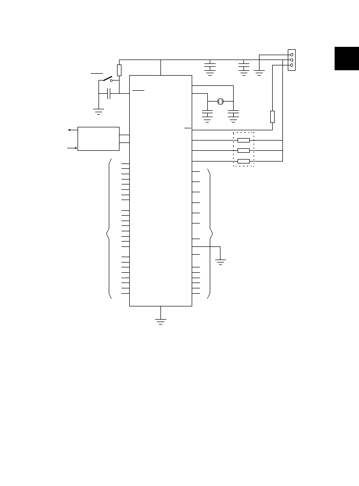
Figure 2-2 MC68HC05X16 `jump to any address' schematic diagram
OSC1
OSC2
IRQ
TCAP2
TCMP2
TCAP1
PB7
PB6
PB5
PB4
PB3
PB2
PB1
PB0
PC7
PC6
PC5
PC4
PC3
PC2
PC1
PC0
VSS
PD7
PD6
PD5
PD4
PD3
PD2
PD1
PD0
PA7
PA6
PA5
PA4
PA3
PA2
PA1
PA0
RESET
VDD
10 k
0.01 mF
10 nF
47 mF
4 MHz
22 pF
10 k
22 pF
P1
GND
+5V
2xV
DD
RESET
VRH
VRL
VPP1
PLMA
PLMB
TCMP1
RDI
TDO
SCLK
10 k
10 k
10 k
optional
3 x 10 k
Connect as required
for the application
8 x 10 k
optional (see note)
8 x 10 k
8 x 10 k
MSB
LSB
Select required address
Note:
These eight resistors are optional; direct connection is possible if pins PA0-PA7, PB0-PB7 and PC0-PC7 are
kept in input mode during application.
MC68HC05X16
26
MC68HC05X16
Rev. 1
MOTOROLA
2-5
MODES OF OPERATION AND PIN DESCRIPTIONS
2
Figure 2-3 MC68HC05X16 `load program in RAM and execute' schematic diagram
OSC1
OSC2
IRQ
TCAP2
TCMP2
TCAP1
PB7
PB6
PB5
PB4
PB3
PB2
PB1
PB0
PC7
PC6
PC5
PC4
PC3
PC2
PC1
PC0
VSS
PD7
PD6
PD5
PD4
PD3
PD2
PD1
PD0
PA7
PA6
PA5
PA4
PA3
PA2
PA1
PA0
RESET
VDD
10 k
0.01 mF
10 nF
47 mF
4 MHz
22 pF
10 k
22 pF
P1
GND
+5V
2xV
DD
RESET
VRH
VRL
VPP1
PLMA
PLMB
TCMP1
RDI
TDO
RS232 level translator
suggested:
MC145406 or MAX232
9600 Bd
RS232
SCLK
10 k
10 k
10 k
optional
3 x 10 k
Connect as required
for the application
Connect as required
for the application
MC68HC05X16
27

MOTOROLA
2-6
MC68HC05X16
Rev. 1
MODES OF OPERATION AND PIN DESCRIPTIONS
2
2.2
Low power modes
The STOP and WAIT instructions have different effects on the programmable timer, the serial
communications interface, the watchdog system, the EEPROM and the A/D converter. These
different effects are described in the following sections.
2.2.1
STOP mode
The STOP instruction places the MCU in its lowest power consumption mode. In STOP mode, the
internal oscillator is turned off (providing the MCAN is `asleep', see
Section 5.5
) halting all internal
processing including timer, serial communications interface and the A/D converter (see flow chart
in
Figure 2-4
). The MCU will wake up from STOP mode only by receipt of an MCAN external
interrupt or by the detection of a reset (logic low on RESET pin or a power-on reset.
The STOP instruction can be executed (i.e. the oscillator can be turned off) only when the MCAN
module is in SLEEP mode. See
Section 5.5
.
During STOP mode, the I-bit in the CCR is cleared to enable external interrupts (see
Section 11.1.5
). The SM bit is cleared to allow nominal speed operation for the 4064 cycles count
while exiting STOP mode (see
Section 2.2.3
).
All other registers and memory remain unaltered and all input/output lines remain unchanged. This
continues until a MCAN interrupt, wired-OR interrupt, external interrupt (IRQ) or reset is sensed,
at which time the internal oscillator is turned on. The interrupt or reset causes the program counter
to vector to the corresponding locations ($3FFA, B and $3FFE, F respectively).
When leaving STOP mode, a t
PORL
internal cycles delay is provided to give the oscillator time to
stabilise before releasing CPU operation. This delay is selectable via a mask option to be either 16
or 4064 cycles. The CPU will resume operation by servicing the interrupt that wakes it up, or by
fetching the reset vector, if reset wakes it up.
Note:
If t
PORL
is selected to be 16 cycles, it is recommended that an external clock signal is
used to avoid problems with oscillator stability while the device is in STOP mode.
The stacking corresponding to an eventual interrupt to go out of STOP mode will only
be executed when going out of STOP mode.
The following list summarizes the effect of STOP mode on the modules of the MC68HC05X16.
≠
The watchdog timer is reset; see
Section 10.1.4.1
≠
The EEPROM acts as read-only memory (ROM); see
Section 3.6
≠
All SCI activity stops; see
Section 7.13
≠
The timer stops counting; see
Section 6.6
≠
The PLM outputs remain at current levels; see
Section 8.3
≠
The A/D converter is disabled; see
Section 9.3
≠
The I-bit in the CCR is cleared
28

MC68HC05X16
Rev. 1
MOTOROLA
2-7
MODES OF OPERATION AND PIN DESCRIPTIONS
2
2.2.2
WAIT mode
The WAIT instruction places the MCU in a low power consumption mode, but WAIT mode
consumes more power than STOP mode. All CPU action is suspended and the watchdog is
disabled, but the timer, A/D and SCI and MCAN systems remain active and operate as normal (see
flow chart in
Figure 2-4
). All other memory and registers remain unaltered and all parallel
input/output lines remain unchanged. The programming or erase mechanism of the EEPROM is
also unaffected, as well as the charge pump high voltage generator.
During WAIT mode the I-bit in the CCR is cleared to enable all interrupts. The INTE bit in the
miscellaneous register (
Section 2.2.3.1
) is not affected by WAIT mode. When any interrupt or reset
is sensed, the program counter vectors to the locations containing the start address of the interrupt
or reset service routine.
Any interrupt or reset condition causes the processor to exit WAIT mode.
If an interrupt exit from WAIT mode is performed, the state of the remaining systems will be
unchanged.
If a reset exit from WAIT mode is performed the entire system reverts to the disabled reset state.
Note:
The stacking corresponding to an eventual interrupt to leave WAIT mode will only be
executed when leaving WAIT mode.
29

MOTOROLA
2-8
MC68HC05X16
Rev. 1
MODES OF OPERATION AND PIN DESCRIPTIONS
2
The following list summarizes the effect of WAIT mode on the modules of the MC68HC05X16.
≠
The watchdog timer functions according to the mask option selected; see
Section 10.1.4.2
≠
The EEPROM is not affected; see
Section 3.7
≠
The SCI is not affected; see
Section 7.14
≠
The timer is not affected; see
Section 6.7
≠
The PLM is not affected; see
Section 8.4
≠
The A/D converter is not affected; see
Section 9.4
≠
The I-bit in the CCR is cleared
≠
The MCAN module is unaffected
2.2.2.1
Power consumption during WAIT mode
Power consumption during WAIT mode depends on how many systems are active. The power
consumption will be highest when all the systems (A/D, timer, EEPROM, SCI and MCAN) are
active, and lowest when the EEPROM erase and programming mechanism, SCI and A/D are
disabled and the MCAN is in SLEEP mode. The timer cannot be disabled in WAIT mode. It is
important that before entering WAIT mode, the programmer sets the relevant control bits for the
individual modules to reflect the desired functionality during WAIT mode.
Power consumption may be further reduced by the use of SLOW mode. (See
Section 2.2.3
).
2.2.3
SLOW mode
The SLOW mode function is controlled by the SM bit in the miscellaneous register at location
$000C. It allows the user to insert, under software control, an extra divide-by-16 between the
oscillator and the internal clock driver (see
Figure 2-5
). This feature allows all the internal
operations to slow down and thus reduces power consumption.
Warning: The SLOW mode function should not be enabled while using the A/D converter or while
erasing/programming the EEPROM unless the internal A/D RC oscillator is turned on.
30
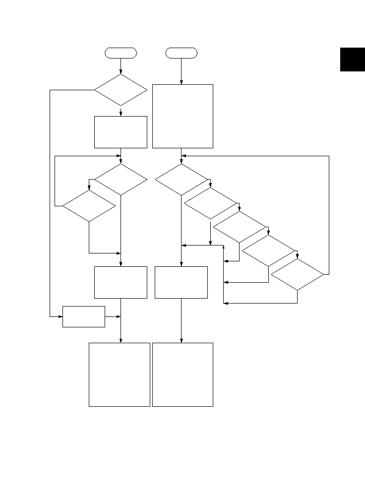
MC68HC05X16
Rev. 1
MOTOROLA
2-9
MODES OF OPERATION AND PIN DESCRIPTIONS
2
Figure 2-4 STOP and WAIT flow charts
Generate watchdog
interrupt
Timer interrupt ?
SCI ?
Stop oscillator and all
clocks.
Clear I bit.
STOP
WAIT
Reset ?
CIRQ,
wired-OR, external
interrupt?
Reset ?
Watchdog active?
(1) Fetch reset vector or
(2) Service interrupt:
a. stack
b. set I-bit
c. vector to interrupt
routine
(1) Fetch reset vector or
(2) Service interrupt:
a. stack
b. set I-bit
c. vector to interrupt
routine
Turn on oscillator.
Wait for time delay to
stabilise
Restart processor clock
YES
NO
YES
YES
YES
YES
YES
YES
NO
NO
NO
NO
NO
NO
Oscillator active. Timer,
SCI, A/D, EEPROM clocks
active. Processor clocks
stopped. Clear I-bit
WOI ?
CIRQ ?
YES
NO
31

MOTOROLA
2-10
MC68HC05X16
Rev. 1
MODES OF OPERATION AND PIN DESCRIPTIONS
2
2.2.3.1
Miscellaneous register
SM -- Slow mode
1 (set)
≠
The system runs at a bus speed 16 times lower than normal (f
OSC
/32,
/64, /128 or /160). SLOW mode affects all sections of the device
(including SCI, A/D and timer) except for the MCAN module.
0 (clear) ≠
The system runs at normal bus speed (f
OSC
/2, /4, /8 or /10).
The SM bit is cleared by external or power-on reset. The SM bit is automatically cleared when
entering STOP mode.
Note:
The bits shown shaded in the above representation are explained individually in the
relevant sections of this manual. The complete register plus an explanation of each bit
can be found in
Section 3.8
.
Figure 2-5 Slow mode divider block diagram
Address
bit 7
bit 6
bit 5
bit 4
bit 3
bit 2
bit 1
bit 0
State
on reset
Miscellaneous
$000C
POR
INTP
INTN
INTE
SFA
SFB
SM
WDOG u001 000u
OSC1
pin
OSC2
pin
Oscillator
f
OSC
Control logic
SM≠bit
˜
2, 4,
Main internal clock
(bit 1, $000C)
MCAN
Note:
The MCAN module clock is unaffected during SLOW mode.
8 and 10
˜
2
˜
16
32

MC68HC05X16
Rev. 1
MOTOROLA
2-11
MODES OF OPERATION AND PIN DESCRIPTIONS
2
2.3
Pin descriptions
2.3.1
VDD and VSS
Power is supplied to the microcontroller using these two pins. VDD is the positive supply and VSS
is ground.
It is in the nature of CMOS designs that very fast signal transitions occur on the MCU pins. These
short rise and fall times place very high short-duration current demands on the power supply. To
prevent noise problems, special care must be taken to provide good power supply bypassing at
the MCU. Bypass capacitors should have good high-frequency characteristics and be as close to
the MCU as possible. Bypassing requirements vary, depending on how heavily the MCU pins are
loaded.
2.3.2
IRQ
This is an input-only pin for external interrupt sources. Interrupt triggering is selected using the
INTP and INTN bits in the miscellaneous register, to be one of four options detailed in
Table 10-3
.
In addition, the external interrupt facility (IRQ) can be disabled using the INTE bit in the
Miscellaneous register (see
Section 3.8
). It is only possible to change the interrupt option bits in
the miscellaneous register while the I-bit is set. Selecting a different interrupt option will
automatically clear any pending interrupts. Further details of the external interrupt procedure can
be found in
Section 10.2.3.2
.
The IRQ pin contains an internal Schmitt trigger as part of its input to improve noise immunity. A
high voltage detector is provided on this pin to select modes of operation other than single-chip
mode. See
Section 2.1
.
2.3.3
RESET
This active low I/O pin is used to reset the MCU. Applying a logic zero to this pin forces the device
to a known start-up state. An external RC-circuit can be connected to this pin to generate a
power-on reset (POR) if required. In this case, the time constant must be great enough (at least
100ms) to allow the oscillator circuit to stabilise. This input has an internal Schmitt trigger to
improve noise immunity. When a reset condition occurs internally, i.e. from the COP watchdog, the
RESET pin provides an active-low open drain output signal that may be used to reset external
hardware.
33

MOTOROLA
2-12
MC68HC05X16
Rev. 1
MODES OF OPERATION AND PIN DESCRIPTIONS
2
2.3.4
MDS
A pull-down device is activated on this pin each time the RESET pin is pulled low. Even after the
RESET pin is pulled high, the pull-down on the MDS pin will remain active until the pin is pulled
high. In single-chip mode MDS can be connected to VSS or left floating. When MDS is tied to V
DD
at the end of reset, it is used to select any mode of operation other than single-chip mode. This
has the same effect as tying IRQ to 2V
DD
. See
Section 2.1
.
Note:
Although this pin can be left floating to select single-chip mode, it is advisable to
hard-connect it to VSS, especially in an electrically noisy environment.
2.3.5
TCAP1
The TCAP1 input controls the input capture 1 function of the on-chip programmable timer system.
2.3.6
TCAP2
The TCAP2 input controls the input capture 2 function of the on-chip programmable timer system.
2.3.7
TCMP1
The TCMP1 pin is the output of the output compare 1 function of the timer system.
2.3.8
TCMP2
The TCMP2 pin is the output of the output compare 2 function of the timer system.
2.3.9
RDI (Receive data in)
The RDI pin is the input pin of the SCI receiver.
2.3.10
TDO (Transmit data out)
The TDO pin is the output pin of the SCI transmitter.
34

MC68HC05X16
Rev. 1
MOTOROLA
2-13
MODES OF OPERATION AND PIN DESCRIPTIONS
2
2.3.11
SCLK
The SCLK pin is the clock output pin of the SCI transmitter.
2.3.12
OSC1, OSC2
These pins provide control input for an on-chip oscillator circuit. A crystal, ceramic resonator or
external clock signal connected to these pins supplies the oscillator clock. The oscillator frequency
(f
OSC
) is divided by two, four, eight or ten to give the internal bus frequency (f
OP
). There is also a
software option which introduces an additional divide by 16 into the oscillator clock, giving an
internal bus frequency of f
OSC
/32, /64, /128 or /160.
2.3.12.1
Crystal
The circuit shown in
Figure 2-6
(a) is recommended when using either a crystal or a ceramic
resonator. An internal feedback resistor is provided on-chip between OSC1 and OSC2.
Figure 2-6
(d) lists the recommended capacitance values. The internal oscillator is designed to
interface with an AT-cut parallel-resonant quartz crystal resonator in the frequency range specified
for f
OSC
(see
Section 12.4
). Use of an external CMOS oscillator is recommended when crystals
outside the specified ranges are to be used. The crystal and associated components should be
mounted as close as possible to the input pins to minimise output distortion and start-up
stabilization time. The manufacturer of the particular crystal being considered should be consulted
for specific information.
2.3.12.2
Ceramic resonator
A ceramic resonator may be used instead of a crystal in cost sensitive applications for frequencies up
to 8MHz external. The circuit shown in
Figure 2-6
(a) is recommended when using either a crystal or a
ceramic resonator.
Figure 2-6
(d) lists the recommended capacitance and feedback resistance values.
The manufacturer of the particular ceramic resonator being considered should be consulted for specific
information. This option is recommended only for applications that operate at an external clock
frequency of 8MHz or less. Any application requiring an external operating frequency greater that
8MHz should use either a crystal oscillator or an external CMOS compatible clock source.
2.3.12.3
External clock
When using an external clock the OSC1 and OSC2 pins should be driven in antiphase, as shown
in
Figure 2-6
(c). The t
OXOV
or t
ILCH
specifications (see
Section 12.4
) do not apply when using an
external clock input. The equivalent specification of the external clock source should be used in
lieu of t
OXOV
or t
ILCH
.
35

MOTOROLA
2-14
MC68HC05X16
Rev. 1
MODES OF OPERATION AND PIN DESCRIPTIONS
2
Figure 2-6 Oscillator connections
Ceramic resonator
2 ≠ 4MHz
Unit
R
S
(typ)
10
W
C
0
40
pF
C
1
4.3
pF
C
OSC1
30
pF
C
OSC2
30
pF
Q
1250
--
Crystal
2MHz
4MHz
Unit
R
S
(max)
400
75
W
C
0
5
7
pF
C
1
8
12
F
C
OSC1
15 ≠ 40
15 ≠ 30
pF
C
OSC2
15 ≠ 30
15 ≠ 25
pF
Q
30 000
40 000
--
OSC1
OSC2
MCU
COSC2
COSC1
OSC1
OSC2
MCU
NC
External
clock
OSC1
OSC2
RS
C1
L
C0
(d) Typical crystal and ceramic resonator parameters
(c) External clock source connections
(b) Crystal equivalent circuit
(a) Crystal/ceramic resonator
oscillator connections
36

MC68HC05X16
Rev. 1
MOTOROLA
2-15
MODES OF OPERATION AND PIN DESCRIPTIONS
2
2.3.12.4
Oscillator division
The external oscillator can run up to 22MHz. For this reason an additional clock predivider is
provided; its division ratio is selected via a mask option (see
Section 1.2
). This allows a CPU clock
two, four, eight or ten times slower than the external clock, provided that SLOW mode has not been
entered. If the device is in SLOW mode, a further divide-by-16 oscillator predivider reduces the
CPU clock frequency to a frequency 32, 64, 128 or 160 times slower than the oscillator clock. The
MCAN is directly clocked with the external oscillator frequency divided by two. A block diagram of
the oscillator divider circuit is given in
Figure 2-7
.
2.3.13
PLMA
The PLMA pin is the output of pulse length modulation converter A.
2.3.14
PLMB
The PLMB pin is the output of pulse length modulation converter B.
Figure 2-7 Oscillator divider block diagram
OSC1
pin
OSC2
pin
Oscillator
MCAN module
˜
16
Control logic
˜
2
SM bit
˜
1
,
˜
2,
˜
4, or
˜
5
f
OSC
/2, /4, /8 or /10
f
OSC
/32, /64,
/128 or /160
MCAN clock
Main internal clock
Mask option
˜
2
37

MOTOROLA
2-16
MC68HC05X16
Rev. 1
MODES OF OPERATION AND PIN DESCRIPTIONS
2
2.3.15
VPP1
The VPP1 pin is the output of the charge pump for the EEPROM1 array.
2.3.16
VRH
The VRH pin is the positive reference voltage for the A/D converter.
2.3.17
VRL
The VRL pin is the negative reference voltage for the A/D converter.
2.3.18
PA0 ≠ PA7/PB0 ≠ PB7/PC0 ≠ PC7
These 24 I/O lines comprise ports A, B and C. The state of any pin is software programmable, and
all the pins are configured as inputs during power-on or reset.
Under software control the PC2 pin can output the internal E-clock (see
Section 4.2
).
Resistive pull downs are provided on port B and/or port C and can be enabled via a mask option
(see
Section 1.2
). Wired-OR interrupt capability is provided on all pins of port B (see
Section 10.2.3.3
).
2.3.19
NWOI
This pin provides another wired-OR interrupt capability in addition to port B. Wired-OR interrupts
are requested when this pin is pulled high (if wired-OR interrupts are enabled), i.e. interrupt
sensitivity on this pin is complementary to sensitivity on the IRQ pin (see
Table 10-3
in
Section 10.2.3.1
). When this pin is not in use it is recommended that it be tied to V
SS
in noisy
conditions. It is not necessary to tie NWOI to V
SS
when there is a negligible amount of noise
present.
2.3.20
PD0/AN0≠PD7/AN7
This 8-bit input only port (D) shares its pins with the A/D converter. When enabled, the A/D
converter uses pins PD0/AN0 ≠ PD7/AN7 as its analog inputs. On reset, the A/D converter is
disabled which forces the port D pins to be input only port pins (see
Section 9.5
).
38

MC68HC05X16
Rev. 1
MOTOROLA
2-17
MODES OF OPERATION AND PIN DESCRIPTIONS
2
2.3.21
VDD1
This pin is the power input for the input comparator of the MCAN module.
2.3.22
VSS1
This pin is the ground connection for the input comparator of the MCAN bus.
2.3.23
VDDH
This pin provides the high voltage reference output for the MCAN bus. The output voltage is equal
to VDD
˜
2.
2.3.24
RX0/RX1
These input pins connect the physical bus lines to the input comparator (receive). When the MCAN
is in SLEEP mode, a dominant level on these pins will wake it up.
2.3.25
TX0/TX1
These output pins connect the output drivers of the MCAN bus to the physical bus lines (transmit).
MCAN bus lines. The bus can have one of two complementary values: dominant or recessive.
During simultaneous transmission of dominant and recessive bits the resulting bus value will be
dominant. For example with a positive logic wired-AND implementation of the bus, the dominant
level would correspond to a logic 0 and the recessive level to a logic 1.
39

MOTOROLA
2-18
MC68HC05X16
Rev. 1
MODES OF OPERATION AND PIN DESCRIPTIONS
2
THIS PAGE LEFT BLANK INTENTIONALLY
40

MC68HC05X16
Rev. 1
MOTOROLA
3-1
MEMORY AND REGISTERS
3
3
MEMORY AND REGISTERS
The MC68HC05X16 MCU is capable of addressing 16384 bytes of memory and registers with its
program counter. The memory map includes 15118 bytes of user ROM (including user vectors),
576 bytes of bootstrap ROM, 352 bytes of RAM and 256 bytes of EEPROM.
3.1
Registers
All the I/O, control and status registers of the MC68HC05X16 are contained within the first 32-byte
block of the memory map, as shown in
Figure 3-1
. MCAN registers are contained in the next 30
bytes of memory.
The miscellaneous register is shown in
Section 3.8
as this register contains bits which are relevant
to several modules.
3.2
RAM
The user RAM comprises 176 bytes of memory, from $0050 to $00FF. This is shared with a 64 byte
stack area. The stack begins at $00FF and may extend down to $00C0. The user RAM also
comprises 176 bytes from $0250 to $02FF which is completely free for the user.
Note:
Using the stack area for data storage or temporary work locations requires care to prevent
the data from being overwritten due to stacking from an interrupt or subroutine call.
3.3
ROM
The user ROM consists of 15118 bytes of ROM mapped as follows:
∑
15102 bytes of user ROM from $0300 to $3DFD
∑
16 bytes of user vectors from $3FF0 to $3FFF
41

MOTOROLA
3-2
MC68HC05X16
Rev. 1
MEMORY AND REGISTERS
3
Figure 3-1 Memory map of the MC68HC05X16
User
Vectors
Port B data register
Port C data register
Port D input data register
Port A data register
$0000
Compare low register 2
A/D data register
Port A data direction register
Port B data direction register
Port C data direction register
E/EEPROM/ECLK control register
A/D status/control register
Pulse length modulation A
Pulse length modulation B
Miscellaneous register
SCI baud rate register
SCI control register 1
SCI control register 2
SCI status register
SCI data register
Timer control register
Timer status register
Capture high register 1
Capture low register 1
Compare high register 1
Compare low register 1
Counter high register
Counter low register
Alternate counter high register
Alternate counter low register
Capture high register 2
Capture low register 2
Compare high register 2
$0001
$0002
$0003
$0004
$0005
$0006
$0007
$0008
$0009
$000A
$000B
$000C
$000D
$000E
$000F
$0010
$0011
$0012
$0013
$0014
$0015
$0016
$0017
$0018
$0019
$001A
$001B
$001C
$001D
$001E
$001F
$0100
Options register
Reserved
Registers
$3FFE≠F
$3FF6≠7
$0000
I/O
(32 bytes)
$0020
$00C0
$0100
$3FF0≠1
Stack
RAM I
(176 bytes)
$0250
$0200
$3DFE
$003E
Bootstrap ROM I
(80 bytes)
ROM
(15102 bytes)
Bootstrap ROM II
(498 bytes)
$0300
$3FF2≠3
OPTR (1 byte)
Non protected (31 bytes)
Protected (224 bytes)
EEPROM
(256 bytes)
$0101
$0120
MC68HC05X16
SCI
Timer overflow
Timer output compare 1& 2
Timer input capture 1& 2
WOI, External IRQ
SWI
Reset/power-on reset
$3FF4≠5
$3FF8≠9
$3FFA≠B
$3FFC≠D
RAM II
176 bytes
MCAN
registers
$0050
CIRQ
MCAN
control registers
10 bytes
MCAN
transmit buffer
10 bytes
MCAN
receive buffer
10 bytes
Ports
7 bytes
EEPROM/ECLK
control
1 byte
PLM system
2 bytes
A/D
converter
2 bytes
Miscellaneous
1 byte
SCI
5 bytes
Timer
14 bytes
$3DFE
Mask options register
$3E00
42
MC68HC05X16
Rev. 1
MOTOROLA
3-3
MEMORY AND REGISTERS
3
3.4
Bootstrap ROM
There are two areas of bootstrap ROM (ROMI and ROMII) located from $0200 to $024F (80 bytes)
and $3DFE to $3FEF (498 bytes) respectively.
Figure 3-2 MCAN module memory map
MCAN
control registers
10 bytes
MCAN
transmit buffer
10 bytes
MCAN
receive buffer
10 bytes
Command register
Status register
Interrupt register
Control register
$0020
Output control register
Acceptance code register
Acceptance mask register
Bus timing register 1
Bus timing register 2
Test register
Identifier
RTR-bit, data length code
Data segment byte 1
Data segment byte 2
Data segment byte 3
Data segment byte 4
Data segment byte 5
Data segment byte 6
Data segment byte 7
Data segment byte 8
$0021
$0022
$0023
$0024
$0025
$0026
$0027
$0028
$0029
$002A
$002B
$002C
$002D
$002E
$002F
$0030
$0031
$0032
$0033
Identifier
RTR-bit, data length code
Data segment byte 1
Data segment byte 2
Data segment byte 3
Data segment byte 4
Data segment byte 5
Data segment byte 6
Data segment byte 7
Data segment byte 8
$0034
$0035
$0036
$0037
$0038
$0039
$003A
$003B
$003C
$003D
MCAN registers
MCAN register blocks
$0020
$0029
$002A
$0033
$0034
$003D
43

MOTOROLA
3-4
MC68HC05X16
Rev. 1
MEMORY AND REGISTERS
3
3.5
EEPROM
The user EEPROM consists of 256 bytes of memory located from address $0100 to $01FF. 255
bytes are general purpose and 1 byte is used by the option register. The non-volatile EEPROM is
byte erasable.
An internal charge pump provides the EEPROM voltage (V
PP1
), which removes the need to supply
a high voltage for erase and programming functions. The charge pump is a capacitor/diode ladder
network which will give a very high impedance output of around 20-30 M
. The voltage of the
charge pump is visible at the VPP1 pin. During normal operation of the device, where
programming/erasing of the EEPROM array will occur, VPP1 should never be connected to either
VDD or VSS as this could prevent the charge pump reaching the necessary programming voltage.
Where it is considered dangerous to leave VPP1 unconnected for reasons of excessive noise in a
system, it may be tied to V
DD
; this will protect the EEPROM data but will also increase power
consumption, and therefore it is recommended that the protect bit function is used for regular
protection of EEPROM data (see
Section 3.5.5
).
In order to achieve a higher degree of security for stored data, there is no capability for bulk or row
erase operations.
The EEPROM control register ($0007) provides control of the EEPROM programming and erase
operations.
Warning: The VPP1 pin should never be connected to VSS, as this could cause permanent
damage to the device.
3.5.1
EEPROM control register
WOIE -- Wired-OR interrupt enable
This bit is used to enable wired-OR interrupts on the NWOI pin and on all port B pins which have
been programmed as inputs. Wired-OR interrupts can only be enabled if the WOI mask option is
selected (see
Section 1.2
). WOIE is forced to zero if this mask option is not selected. Power-on
reset clears the WOIE bit.
1 (set)
≠
Wired-OR interrupts are enabled (provided that wired-OR interrupts
have been selected as a mask option).
0 (clear) ≠
Wired-OR interrupts are disabled.
Address
bit 7
bit 6
bit 5
bit 4
bit 3
bit 2
bit 1
bit 0
State
on reset
EEPROM/ECLK control
$0007
WOIE
CAF
0
0
ECLK E1ERA E1LAT E1PGM 0000 0000
44

MC68HC05X16
Rev. 1
MOTOROLA
3-5
MEMORY AND REGISTERS
3
CAF -- MCAN asleep flag
This flag is set by the MCU when the MCAN module enters SLEEP mode. This is the only
indication that the MCAN is asleep (see
Section 5.5
). The bit is cleared when the MCAN wakes up.
1 (set)
≠
The MCAN module is in SLEEP mode.
0 (clear) ≠
The MCAN module is not in SLEEP mode.
ECLK -- External clock option bit
See
Section 4.3
for a description of this bit.
E1ERA -- EEPROM erase/programming bit
Providing the E1LAT and E1PGM bits are at logic one, this bit indicates whether the access to the
EEPROM is for erasing or programming purposes.
1 (set)
≠
An erase operation will take place.
0 (clear) ≠
A programming operation will take place.
Once the program/erase EEPROM address has been selected, E1ERA cannot be changed.
E1LAT -- EEPROM programming latch enable bit
1 (set)
≠
Address and data can be latched into the EEPROM for further
program or erase operations, providing the E1PGM bit is cleared.
0 (clear) ≠
Data can be read from the EEPROM. The E1ERA bit and the E1PGM
bit are reset to zero when E1LAT is `0'.
STOP, power-on and external reset clear the E1LAT bit.
Note:
After the t
ERA1
erase time or t
PROG1
programming time, the E1LAT bit has to be reset
to zero in order to clear the E1ERA bit and the E1PGM bit.
E1PGM -- EEPROM charge pump enable/disable
1 (set)
≠
Internal charge pump generator switched on.
0 (clear) ≠
Internal charge pump generator switched off.
When the charge pump generator is on, the resulting high voltage is applied to the EEPROM array.
This bit cannot be set before the data is selected, and once this bit has been set it can only be
cleared by clearing the E1LAT bit.
A summary of the effects of setting/clearing bits 0, 1 and 2 of the control register are give in
Table 3-1
.
Note:
Not all combinations are shown in
Table 3-1
, since the E1PGM and E1ERA bits are
cleared when the E1LAT bit is at zero, resulting in a read condition.
45

MOTOROLA
3-6
MC68HC05X16
Rev. 1
MEMORY AND REGISTERS
3
3.5.2
EEPROM read operation
To be able to read from EEPROM, the E1LAT bit has to be at logic zero, as shown in
Table 3-1
.
While this bit is at logic zero, the E1PGM bit and the E1ERA bit are permanently reset to zero and
the 256 bytes of EEPROM may be read as if it were a normal ROM area. The internal charge pump
generator is automatically switched off since the E1PGM bit is reset.
If a read operation is executed while the E1LAT bit is set (erase or programming sequence), data
resulting from the operation will be $FF.
Note:
When not performing any programming or erase operation, it is recommended that
EEPROM should remain in the read mode (E1LAT = 0)
3.5.3
EEPROM erase operation
To erase the contents of a byte of the EEPROM, the following steps should be taken:
1
Set the E1LAT bit.
2
Set the E1ERA bit (1& 2 may be done simultaneously with the same
instruction).
3
Write address/data to the EEPROM address to be erased.
4
Set the E1PGM bit.
5
Wait for a time t
ERA1
.
6
Reset the E1LAT bit (to logic zero).
While an erase operation is being performed, any access of the EEPROM array will not be
successful.
The erased state of the EEPROM is $FF and the programmed state is $00.
Note:
Data written to the address to be erased is not used, therefore its value is not significant.
Table 3-1 EEPROM control bits description
E1ERA
E1LAT
E1PGM
Description
0
0
0
Read condition
0
1
0
Ready to load address/data for program/erase
0
1
1
Byte programming in progress
1
1
0
Ready for byte erase (load address)
1
1
1
Byte erase in progress
46

MC68HC05X16
Rev. 1
MOTOROLA
3-7
MEMORY AND REGISTERS
3
If a second word is to be erased, it is important that the E1LAT bit be reset before restarting the
erasing sequence, otherwise any write to a new address will have no effect. This condition provides
a higher degree of security for the stored data.
User programs must be running from the RAM or ROM as the EEPROM will have its address and
data buses latched.
3.5.4
EEPROM programming operation
To program a byte of EEPROM, the following steps should be taken:
1
Set the E1LAT bit.
2
Write address/data to the EEPROM address to be programmed.
3
Set the E1PGM bit.
4
Wait for time t
PROG1
.
5
Reset the E1LAT bit (to logic zero).
While a programming operation is being performed, any access of the EEPROM array will not be
successful.
Warning: To program a byte correctly, it has to have been previously erased.
If a second word is to be programmed, it is important that the E1LAT bit be reset before restarting
the programming sequence otherwise any write to a new address will have no effect. This condition
provides a higher degree of security for the stored data.
User programs must be running from the RAM or ROM as the EEPROM will have its address and
data buses latched.
Note:
224 bytes of EEPROM (address $0120 to $01FF) can be program and erase protected
under the control of bit 1 of the OPTR register detailed in
Section 3.5.5
.
3.5.5
Options register (OPTR)
This register (OPTR), located at $0100, contains the secure and protect functions for the EEPROM
and allows the user to select options in a non-volatile manner. The contents of the OPTR register
are loaded into data latches with each power-on or external reset.
(1) This register is implemented in EEPROM; therefore reset has no effect on the individual bits.
Address
bit 7
bit 6
bit 5
bit 4
bit 3
bit 2
bit 1
bit 0
State
on reset
Options (OPTR)
(1)
$0100
EE1P
SEC Not affected
47

MOTOROLA
3-8
MC68HC05X16
Rev. 1
MEMORY AND REGISTERS
3
EE1P ≠ EEPROM protect bit
In order to achieve a higher degree of protection, the EEPROM is effectively split into two parts,
both working from the VPP1 charge pump. Part 1 of the EEPROM array (32 bytes from $0100 to
$011F) cannot be protected; part 2 (224 bytes from $0120 to $01FF) is protected by the EE1P bit
of the options register.
1 (set)
≠
Part 2 of the EEPROM array is not protected; all 256 bytes of EEPROM
can be accessed for any read, erase or programming operations
0 (clear) ≠
Part 2 of the EEPROM array is protected; any attempt to erase or
program a location will be unsuccessful
When this bit is set (erased), the protection will remain until the next power-on or external reset.
EE1P can only be written to `0' when the ELAT bit in the EEPROM control register is set.
SEC ≠ Security bit
This high security bit allows the user to secure the EEPROM data from external accesses. When
the SEC bit is at `0', the EEPROM contents are secured by preventing any entry to test mode. The
only way to erase the SEC bit to `1' externally is to enter bootstrap mode, at which time the entire
EEPROM contents will be erased. When the SEC bit is changed, its new value will have no effect
until the next external or power-on reset.
3.6
EEPROM during STOP mode
When entering STOP mode, the EEPROM is automatically set to the read mode and the VPP1
high voltage charge pump generator is automatically disabled.
3.7
EEPROM during WAIT mode
The EEPROM is not affected by WAIT mode. Any program/erase operation will continue as in
normal operating mode. The charge pump is not affected by WAIT mode, therefore it is possible to
wait the t
ERA1
erase time or t
PROG1
programming time in WAIT mode.
Under normal operating conditions, the charge pump generator is driven by the internal CPU
clocks. When the operating frequency is low, e.g. during slow mode (see
Figure 3.8
) or during
WAIT mode, the clocking should be done by the internal A/D RC oscillator. The RC oscillator is
enabled by setting the ADRC bit of the A/D status/control register at $0009.
48

MC68HC05X16
Rev. 1
MOTOROLA
3-9
MEMORY AND REGISTERS
3
(1)
The POR bit is set each time there is a power-on reset.
(2)
The state of the WDOG bit after reset is dependent on the mask option selected; 1=watchdog enabled, 0=watchdog disabled.
(3)
This register is implemented in EEPROM; therefore reset has no effect on the individual bits.
Table 3-2 MC68HC05X16 register outline
Register name
Address
bit 7
bit 6
bit 5
bit 4
bit 3
bit 2
bit 1
bit 0
State on
reset
Port A data (PORTA)
$0000
Undefined
Port B data (PORTB)
$0001
Undefined
Port C data (PORTC)
$0002
PC2/
ECLK
Undefined
Port D data (PORTD)
$0003
PD7
PD6
PD5
PD4
PD3
PD2
PD1
PD0
Undefined
Port A data direction (DDRA)
$0004
0000 0000
Port B data direction (DDRB)
$0005
0000 0000
Port C data direction (DDRC)
$0006
0000 0000
EEPROM/ECLK control
$0007
WOIE
CAF
0
0
ECLK E1ERA E1LAT E1PGM 0000 0000
A/D data (ADDATA)
$0008
0000 0000
A/D status/control (ADSTAT)
$0009
COCO ADRC ADON
0
CH3
CH2
CH1
CH0
0000 0000
Pulse length modulation A (PLMA)
$000A
0000 0000
Pulse length modulation B (PLMB)
$000B
0000 0000
Miscellaneous
$000C
POR
(1)
INTP
INTN
INTE
SFA
SFB
SM
WDOG
(2)
u001 000u
SCI baud rate (BAUD)
$000D
SPC1
SPC0
SCT1
SCT0
SCT0
SCR2
SCR1
SCR0
00uu uuuu
SCI control 1 (SCCR1)
$000E
R8
T8
M
WAKE CPOL
CPHA
LBCL
Undefined
SCI control 2 (SCCR2)
$000F
TIE
TCIE
RIE
ILIE
TE
RE
RWU
SBK
0000 0000
SCI status (SCSR)
$0010
TDRE
TC
RDRF
IDLE
OR
NF
FE
1100 000u
SCI data (SCDR)
$0011
0000 0000
Timer control (TCR)
$0012
ICIE
OCIE
TOIE
FOLV2 FOLV1
OLV2
IEDG1 OLVL1 0000 00u0
Timer status (TSR)
$0013
ICF1
OCF1
TOF
ICF2
OCF2
Undefined
Input capture high 1
$0014
Undefined
Input capture low 1
$0015
Undefined
Output compare high 1
$0016
Undefined
Output compare low 1
$0017
Undefined
Timer counter high
$0018
1111 1111
Timer counter low
$0019
1111 1100
Alternate counter high
$001A
1111 1111
Alternate counter low
$001B
1111 1100
Input capture high 2
$001C
Undefined
Input capture low 2
$001D
Undefined
Output compare high 2
$001E
Undefined
Output compare low 2
$001F
Undefined
Options (OPTR)
(3)
$0100
EE1P
SEC
Not affected
49

MOTOROLA
3-10
MC68HC05X16
Rev. 1
MEMORY AND REGISTERS
3
(1)
These registers can only be accessed when the reset request bit in the control register is set.
Table 3-3 MCAN register outline
Register name
Address
bit 7
bit 6
bit 5
bit 4
bit 3
bit 2
bit 1
bit 0
State on
reset
Control (CCNTRL)
$0020
MODE
SPD
OIE
EIE
TIE
RIE
RR
0u - u uuu1
Command (CCOM)
$0021
RX0
RX1
COMPSEL
SLEEP
COS
RRB
AT
TR
00u0 0000
Status (CSTAT)
$0022
BS
ES
TS
RS
TCS
TBA
DO
RBS
uu00 1100
Interrupt (CINT)
$0023
WIF
OIF
EIF
TIF
RIF
- - - 0 0000
Acceptance code (CACC)
(1)
$0024
AC7
AC6
AC5
AC4
AC3
AC2
AC1
AC0
Undefined
Acceptance mask (CACM)
(1)
$0025
AM7
AM6
AM5
AM4
AM3
AM2
AM1
AM0
Undefined
Bus timing 0 (CBT0)
(1)
$0026
SJW1
SJW0
BRP5
BRP4
BRP3
BRP2
BRP1
BRP0
Undefined
Bus timing 1 (CBT1)
(1)
$0027
SAMP TSEG22TSEG21TSEG20TSEG13TSEG12TSEG11TSEG10 Undefined
Output control (COCNTRL)
(1)
$0028
OCTP1 OCTN1
OCPOL1
OCTP0 OCTN0
OCPOL0
OCM1 OCM0 Undefined
(reserved)
$0029
Transmit buffer identifier (TBI)
$002A
ID10
ID9
ID8
ID7
ID6
ID5
ID4
ID3
Undefined
RTR-bit, data length code (TRTDL)
$002B
ID2
ID1
ID0
RTR
DLC3
DLC2
DLC1
DLC0
Undefined
Transmit data segment 1 (TDS1)
$002C
DB7
DB6
DB5
DB4
DB3
DB2
DB1
DB0
Undefined
Transmit data segment 2 (TDS2)
$002D
DB7
DB6
DB5
DB4
DB3
DB2
DB1
DB0
Undefined
Transmit data segment 3 (TDS3)
$002E
DB7
DB6
DB5
DB4
DB3
DB2
DB1
DB0
Undefined
Transmit data segment 4 (TDS4)
$002F
DB7
DB6
DB5
DB4
DB3
DB2
DB1
DB0
Undefined
Transmit data segment 5 (TDS5)
$0030
DB7
DB6
DB5
DB4
DB3
DB2
DB1
DB0
Undefined
Transmit data segment 6 (TDS6)
$0031
DB7
DB6
DB5
DB4
DB3
DB2
DB1
DB0
Undefined
Transmit data segment 7 (TDS7)
$0032
DB7
DB6
DB5
DB4
DB3
DB2
DB1
DB0
Undefined
Transmit data segment 8 (TDS8)
$0033
DB7
DB6
DB5
DB4
DB3
DB2
DB1
DB0
Undefined
Receive buffer identifier (RBI)
$0034
ID10
ID9
ID8
ID7
ID6
ID5
ID4
ID3
Undefined
RTR-bit, data length code (RRTDL)
$0035
ID2
ID1
ID0
RTR
DLC3
DLC2
DLC1
DLC0
Undefined
Receive data segment 1 (RDS1)
$0036
DB7
DB6
DB5
DB4
DB3
DB2
DB1
DB0
Undefined
Receive data segment 2 (RDS2)
$0037
DB7
DB6
DB5
DB4
DB3
DB2
DB1
DB0
Undefined
Receive data segment 3 (RDS3)
$0038
DB7
DB6
DB5
DB4
DB3
DB2
DB1
DB0
Undefined
Receive data segment 4 (RDS4)
$0039
DB7
DB6
DB5
DB4
DB3
DB2
DB1
DB0
Undefined
Receive data segment 5 (RDS5)
$003A
DB7
DB6
DB5
DB4
DB3
DB2
DB1
DB0
Undefined
Receive data segment 6 (RDS6)
$003B
DB7
DB6
DB5
DB4
DB3
DB2
DB1
DB0
Undefined
Receive data segment 7 (RDS7)
$003C
DB7
DB6
DB5
DB4
DB3
DB2
DB1
DB0
Undefined
Receive data segment 8 (RDS8)
$003D
DB7
DB6
DB5
DB4
DB3
DB2
DB1
DB0
Undefined
50

MC68HC05X16
Rev. 1
MOTOROLA
3-11
MEMORY AND REGISTERS
3
3.8
Miscellaneous register
POR -- Power-on reset bit (see
Section 10.1
)
This bit is set each time the device is powered on. Therefore, the state of the POR bit allows the
user to make a software distinction between a power-on and an external reset. This bit cannot be
set by software and is cleared by writing it to zero.
1 (set)
≠
A power-on reset has occurred.
0 (clear) ≠
No power-on reset has occurred.
INTP, INTN -- External interrupt sensitivity options (see
Section 10.2
)
These two bits allow the user to select which edge the IRQ pin and WOI will be sensitive to (see
Table 3-4
). Both bits can be written to only while the I-bit is set, and are cleared by power-on or
external reset, thus the device is initialised with negative edge and low level sensitivity.
INTE -- External interrupt enable (see
Section 10.2
)
1 (set)
≠
External interrupt function (IRQ) enabled.
0 (clear) ≠
External interrupt function (IRQ) disabled.
The INTE bit can be written to only while the I-bit is set, and is set by power-on or external reset,
thus enabling the external interrupt function.
SFA -- Slow or fast mode selection for PLMA (see
Section 8.1
)
1 (set)
≠
Slow mode PLMA (4096 x timer clock period).
0 (clear) ≠
Fast mode PLMA (256 x timer clock period).
(1) The POR bit is set each time there is a power-on reset.
(2) The state of the WDOG bit after reset is dependent on the mask option selected; 1=watchdog enabled, 0=watchdog disabled.
Address
bit 7
bit 6
bit 5
bit 4
bit 3
bit 2
bit 1
bit 0
State
on reset
Miscellaneous
$000C
POR
(1)
INTP
INTN
INTE
SFA
SFB
SM
WDOG
(2)
u001 000u
Table 3-4 IRQ and WOI sensitivity
INTP
INTN
IRQ sensitivity
WOI interrupt options
0
0
Negative edge and low level sensitive
Positive edge and high level sensitive
0
1
Negative edge only
Positive edge only
1
0
Positive edge only
Negative edge only
1
1
Positive and negative edge sensitive
Positive and negative edge sensitive
51

MOTOROLA
3-12
MC68HC05X16
Rev. 1
MEMORY AND REGISTERS
3
SFB -- Slow or fast mode selection for PLMB (see
Section 8.1
)
1 (set)
≠
Slow mode PLMB (4096 x timer clock period).
0 (clear) ≠
Fast mode PLMB (256 x timer clock period).
Note:
The highest speed of the PLM system corresponds to the frequency of the TOF bit
being set, multiplied by 256. The lowest speed of the PLM system corresponds to the
frequency of the TOF bit being set, multiplied by 16.
Warning: Because the SFA bit and SFB bit are not double buffered, it is mandatory to set the SFA
bit and the SFB bit to the desired values before writing to the PLM registers; not doing
so could temporarily give incorrect values at the PLM outputs.
SM -- Slow mode (see
Section 2.2.3
)
1 (set)
≠
The system runs at a bus speed 16 times lower than normal
(f
OSC
/32). SLOW mode affects all sections of the device, including
SCI, A/D and timer.
0 (clear) ≠
The system runs at normal bus speed (f
OSC
/2).
The SM bit is cleared by external or power-on reset. The SM bit is automatically cleared when
entering STOP mode.
WDOG -- Watchdog enable/disable (see
Section 10.1.4
)
The WDOG bit can be used to enable the watchdog timer previously disabled by a mask option.
Following a watchdog reset the state of the WDOG bit is as defined by the mask option specified.
1 (set)
≠
Watchdog counter cleared and enabled.
0 (clear) ≠
The watchdog cannot be disabled by software; writing a zero to this
bit has no effect.
52

MC68HC05X16
Rev. 1
MOTOROLA
4-1
INPUT/OUTPUT PORTS
4
4
INPUT/OUTPUT PORTS
In single-chip mode, the MC68HC05X16 has a total of 24 I/O lines, arranged as three 8-bit ports
(A, B and C), and eight input-only lines, arranged as one 8-bit port (D). Each I/O line is individually
programmable as either input or output, under the software control of the data direction registers.
The 8-bit input-only port (D) shares its pins with the A/D converter, when the A/D converter is
enabled. To avoid glitches on the output pins, data should be written to the I/O port data register
before writing ones to the corresponding data direction register bits to set the pins to output mode.
4.1
Input/output programming
The bidirectional port lines may be programmed as inputs or outputs under software control. The
direction of each pin is determined by the state of the corresponding bit in the port data direction
register (DDR). Each port has an associated DDR. Any I/O port pin is configured as an output if
its corresponding DDR bit is set to a logic one. A pin is configured as an input if its corresponding
DDR bit is cleared to a logic zero.
At power-on or reset, all DDRs are cleared, thus configuring all port pins as inputs. The data
direction registers can be written to or read by the MCU. During the programmed output state, a
read of the data register actually reads the value of the output data latch and not the I/O pin. The
operation of the standard port hardware is shown schematically in
Figure 4-1
.
53

MOTOROLA
4-2
MC68HC05X16
Rev. 1
INPUT/OUTPUT PORTS
4
Table 4-1
shows the effect of reading from or writing to an I/O pin in various circumstances. Note
that the read/write signal shown is internal and not available to the user.
4.2
Ports A and B
These ports are standard M68HC05 bidirectional I/O ports, each comprising a data register and a
data direction register.
Reset does not affect the state of the data register, but clears the data direction register, thereby
returning all port pins to input mode. Writing a `1' to any DDR bit sets the corresponding port pin
to output mode.
Wired-OR interrupts are provided on all pins of port B. If WOIE is enabled, any combination of high
logic levels on port B pins which are programmed as inputs will trigger an external interrupt. See
Section 10.2.3.2
.
Figure 4-1 Standard I/O port structure
Table 4-1 I/O pin states
R/W
DDRn
Action of MCU write to/read of data bit
0
0
The I/O pin is in input mode. Data is written into the output data latch.
0
1
Data is written into the output data latch, and output to the I/O pin.
1
0
The state of the I/O pin is read.
1
1
The I/O pin is in output mode. The output data latch is read.
Latched data
register bit
DDRn
DATA
Input
buffer
Output
buffer
O/P
data
buffer
M68HC05 inter
nal connections
DDRn
DATA
I/O Pin
1
0
0
1
1
1
0
0
tristate
0
1
tristate
I/O
Pin
Output
Input
Data direction
register bit
54

MC68HC05X16
Rev. 1
MOTOROLA
4-3
INPUT/OUTPUT PORTS
4
A mask option is provided to enable resistive pull downs on all port B pins that are programmed
as inputs.
4.3
Port C
In addition to the standard port functions described for ports A and B, port C pin 2 can be
configured, using the ECLK bit of the EEPROM/ECLK control register, to output the CPU clock. If
this is selected the corresponding DDR bit is automatically set and bit 2 of port C will always read
the output data latch. The other port C pins are not affected by this feature.
A mask option is provided to enable resistive pull downs on all port C pins that are programmed
as inputs.
ECLK -- External clock option bit
1 (set)
≠
ECLK CPU clock is output on PC2.
0 (clear)
≠
ECLK CPU clock is not output on PC2; port C acts as a normal I/O port.
The ECLK bit is cleared by power-on or external reset. It is not affected by the execution of a STOP
or WAIT instruction.
The timing diagram of the clock output is shown in
Figure 4-2
.
Address
bit 7
bit 6
bit 5
bit 4
bit 3
bit 2
bit 1
bit 0
State
on reset
EEPROM/ECLK control
$0007
0
0
0
0
ECLK E1ERA E1LAT E1PGM 0000 0000
Figure 4-2 ECLK timing diagram
Internal clock (PHI2)
External clock (ECLK/PC2)
Output port (if write to output port)
55

MOTOROLA
4-4
MC68HC05X16
Rev. 1
INPUT/OUTPUT PORTS
4
4.4
Port D
This 8-bit input-only port shares its pins with the A/D converter subsystem. When the A/D
converter is enabled, pins PD0-PD7 read the eight analog inputs to the A/D converter. Port D can
be read at any time, however, if it is read during an A/D conversion sequence noise, may be
injected on the analog inputs, resulting in reduced accuracy of the A/D. Furthermore, performing
a digital read of port D with levels other than V
DD
or V
SS
on the port D pins will result in greater
power dissipation during the read cycle.
As port D is an input-only port there is no DDR associated with it. Also, at power up or external
reset, the A/D converter is disabled, thus the port is configured as a standard input-only port.
Note:
It is recommended that all unused input ports and I/O ports be tied to an appropriate
logic level (i.e. either V
DD
or V
SS
).
4.5
Port registers
The following sections explain in detail the individual bits in the data and control registers
associated with the ports.
4.5.1
Port data registers A and B (PORTA and PORTB)
Each bit can be configured as input or output via the corresponding data direction bit in the port
data direction register (DDRx).
The state of the port data registers following reset is not defined.
Address
bit 7
bit 6
bit 5
bit 4
bit 3
bit 2
bit 1
bit 0
State
on reset
Port A data (PORTA)
$0000
Undefined
Port B data (PORTB)
$0001
Undefined
56

MC68HC05X16
Rev. 1
MOTOROLA
4-5
INPUT/OUTPUT PORTS
4
4.5.2
Port data register C (PORTC)
Each bit can be configured as input or output via the corresponding data direction bit in the port
data direction register (DDRx).
In addition, bit 2 of port C is used to output the CPU clock if the ECLK bit in the EEPROM
CTL/ECLK register is set (see
Section 4.3
).
The state of the port data registers following reset is not defined.
4.5.3
Port data register D (PORTD)
All the port D bits are input-only and are shared with the A/D converter. The function of each bit is
determined by the ADON bit in the A/D status/control register.
The state of the port data registers following reset is not defined.
4.5.4
A/D status/control register
ADON -- A/D converter on
1 (set)
≠
A/D converter is switched on; all port D pins act as analog inputs for
the A/D converter.
0 (clear) ≠
A/D converter is switched off; all port D pins act as input only pins.
Reset clears the ADON bit, thus configuring port D as an input only port.
Address
bit 7
bit 6
bit 5
bit 4
bit 3
bit 2
bit 1
bit 0
State
on reset
Port C data (PORTC)
$0002
PC2/
ECLK
Undefined
Address
bit 7
bit 6
bit 5
bit 4
bit 3
bit 2
bit 1
bit 0
State
on reset
Port D data (PORTD)
$0003
PD7
PD6
PD5
PD4
PD3
PD2
PD1
PD0
Undefined
Address
bit 7
bit 6
bit 5
bit 4
bit 3
bit 2
bit 1
bit 0
State
on reset
A/D status/control
$0009
COCO ADRC ADON
0
CH3
CH2
CH1
CH0
0000 0000
57

MOTOROLA
4-6
MC68HC05X16
Rev. 1
INPUT/OUTPUT PORTS
4
4.5.5
Data direction registers (DDRA, DDRB and DDRC)
Writing a `1' to any bit configures the corresponding port pin as an output; conversely, writing any
bit to `0' configures the corresponding port pin as an input.
Reset clears these registers, thus configuring all ports as inputs.
4.6
Other port considerations
All output ports can emulate `open-drain' outputs. This is achieved by writing a zero to the relevant
output port latch. By toggling the corresponding data direction bit, the port pin will either be an
output zero or tri-state (an input). This is shown diagrammatically in
Figure 4-3
.
When using a port pin as an `open-drain' output, certain precautions must be taken in the user
software. If a read-modify-write instruction is used on a port where the `open-drain' is assigned and
the pin at this time is programmed as an input, it will read it as a `one'. The read-modify-write
instruction will then write this `one' into the output data latch on the next cycle. This would cause
the `open-drain' pin not to output a `zero' when desired.
Note:
`Open-drain' outputs should not be pulled above V
DD
.
Address
bit 7
bit 6
bit 5
bit 4
bit 3
bit 2
bit 1
bit 0
State
on reset
Port A data direction (DDRA)
$0004
0000 0000
Port B data direction (DDRB)
$0005
0000 0000
Port C data direction (DDRC)
$0006
0000 0000
58

MC68HC05X16
Rev. 1
MOTOROLA
4-7
INPUT/OUTPUT PORTS
4
Figure 4-3 Port logic levels
DDRn
A
Y
(b)
1
0
0
Normal operation ≠ tri state
1
1
1
0
0
tri state
0
1
tri state
1
0
low
`Open-drain'
1
1
--
0
0
high
0
1
high
Y
A
Read buffer output
Data direction register bit DDRn
Px0
VDD
V
DD
DDRx, bit 0 = 0
Portx, bit 0 = 0
DDRx, bit 0 = 0
Portx, bit 0 = 0
(c)
(a)
`Open-drain' output
59

MOTOROLA
4-8
MC68HC05X16
Rev. 1
INPUT/OUTPUT PORTS
4
THIS PAGE LEFT BLANK INTENTIONALLY
60

MC68HC05X16
Rev. 1
MOTOROLA
5-1
MOTOROLA CAN MODULE (MCAN)
5
5
MOTOROLA CAN MODULE (MCAN)
The MCAN includes all hardware modules necessary to implement the CAN transfer layer, which
represents the kernel of the CAN bus protocol as defined by BOSCH GmbH, the originators of the
CAN specification. For full details of the CAN protocol please refer to the published specifications.
Up to the message level, the MCAN is totally compatible with the full CAN implementation.
Functional differences are related to the object layer only. Whereas a full CAN controller provides
dedicated hardware for handling a set of messages, the MCAN is restricted to receiving and/or
transmitting messages on a message by message basis.
The MCAN will never initiate an overload frame. If the MCAN starts to receive a valid message
(one that passes the acceptance filter) and there is no receive buffer available for it then the
overrun flag in the CPU status register will be set. The MCAN will respond to overload frames
generated by other CAN nodes, as required by the CAN protocol. A summary of all the MCAN
frame formats is given in
Figure 5-2
for reference. A diagram of the major blocks of the MCAN is
shown in
Figure 5-1
.
Figure 5-1 MCAN block diagram
Interface
management
logic
Transmit
buffer
Receive
buffer 0
Receive
buffer 1
Bit timing
logic
Transceive
logic
Bit stream
processor
Error
management
logic
Line
interface
logic
Microprocessor related logic
Bus line related logic
MCAN
bus
line
61

MO
T
O
R
OLA
5-2
MC68HC05X16
Re
v
.
1
MOTOR
OLA CAN MODULE (MCAN)
5
Figure 5-2
MCAN fr
ame f
o
r
mats
Star
t of fr
ame
ID10
ID0 RT
R
RB1 RB0 DLC3
DLC0
CRC Del Ac
kno
wledge
Ac
k Del
d
d d d
r
r r r r r r r r
Identifier
Acceptance
Stored in buffers
Reser
v
ed bits
Data
Stored in transmit/receive buffers
Bit stuffing
Arbitration field
Control field
CRC field
CRC
End of frame
Data frame
(number of bits = 44 + 8N)
11
4
6
12
8
8
16
7
15
8N (0
N
8)
Data field
filtering
length
code
Star
t of fr
ame
ID10
ID0 RT
R
RB1 RB0 DLC3
DLC0
CRC Del Ac
kno
wledge
Ac
k Del
d
r d d
r
r r r r r r r r
Arbitration field
Control field
CRC field
CRC
End of frame
Remote frame
(number of bits = 44)
11
4
6
12
16
7
15
Note:
A remote frame is identical to a
data frame, except that the RTR
bit is recessive, and there is no
data field.
62

MC68HC05X16
Re
v
.
1
MO
T
O
R
OLA
5-3
MOTOR
OLA CAN MODULE (MCAN)
5
Figure 5-2
MCAN fr
ame f
o
r
mats (Contin
ued)
Error flag
Error frame
Note:
An error frame can start
anywhere in the middle of a
frame.
r r r r r r r r
d d d d d d d
d d
8
6
6
Echo
error flag
Error delimiter
Inter-frame space
or
overload frame
Data frame
or
remote frame
INT
Inter-frame space
r
r r r d
r r r r r r r r r r r r r
r
8
3
Suspend
transmit
Bus idle
r
r
r
r
r
Data frame
or
remote frame
Any frame
Star
t of fr
ame
Note:
INT = Intermission
Suspend transmission is only for
error passive nodes.
Overload flag
Overload frame
r r r
d d d d d d d r r r r r
8
6
Overload delimiter
Inter-frame space
or
error frame
End of frame
or
error delimiter
Note:
An overload frame can only start
at the end of a frame.
Maximum echo of overload flag
is one bit.
or
overload delimiter
63

MOTOROLA
5-4
MC68HC05X16
Rev. 1
MOTOROLA CAN MODULE (MCAN)
5
5.1
TBF ≠ Transmit buffer
The transmit buffer is an interface between the CPU and the bit stream processor (BSP) and is
able to store a complete message. The buffer is written by the CPU and read by the BSP. The CPU
may access this buffer whenever transmit buffer access is set to released. On requesting a
transmission (by setting transmission request in the MCAN command register to present) transmit
buffer access is set to locked, giving the BSP exclusive access to this buffer. The transmit buffer is
released after the message transfer has been completed or aborted.
The TBF is 10 bytes long and holds the identifier (1 byte), the control field (1 byte) and the data
field (maximum length 8 bytes). The buffer is implemented as a single-ported RAM, with mutually
exclusive access by the CPU and the BSP.
5.2
RBF ≠ Receive buffer
The receive buffer is an interface between the BSP and the CPU and stores a message received
from the bus line. Once filled by the BSP and allocated to the CPU (by the IML), the receive buffer
cannot be used to store subsequent received messages until the CPU has acknowledged the
reading of the buffer's contents. Thus, unless the CPU releases a receive buffer within a protocol
defined time frame, future messages to be received may be lost.
To reduce the requirements on the CPU, two receive buffers (RBF0 and RBF1) are implemented.
While one receive buffer is allocated to the CPU, the BSP may write to the other buffer. RBF0 and
RBF1 are each 10 bytes long and hold the identifier (1 byte), the control field (1 byte) and the data
field (maximum length 8 bytes). The buffers are implemented as single-ported RAMs with mutually
exclusive access from the CPU and the BSP. The BSP signals the MCU to read the receive buffer
only when the message being received has an identifier that passes the acceptance filter. Note
that a message being transmitted will be automatically written to the receive buffer if the identifier
passes the acceptance filter. This is because it cannot be known, until after the first byte has been
stored, whether or not the transmitting node will lose arbitration to another node.
5.3
Interface to the MC68HC05X16 CPU
The MCAN handles all the communication transactions flowing across the serial bus. For example,
the CPU merely places a message to be transmitted into the transmit buffer and sets the TR bit.
The MCAN will begin transmitting the message when it has determined that the bus is idle. In the
event of a transmission error, the MCAN will initiate a repeated transmission automatically.
64

MC68HC05X16
Rev. 1
MOTOROLA
5-5
MOTOROLA CAN MODULE (MCAN)
5
In a similar manner, the CPU module is notified that a message has been received only if it was
error free. If any error occurs, the MCAN signals the error within the CAN protocol without CPU
intervention.
The MCAN within the MC68HC05X16 is controlled using a block of 30 registers. This comprises
10 control registers, 10 Transmit buffer registers and 10 receive buffer registers. These registers
are memory mapped between $20 and $3D (see
Figure 5-3
).
Note:
There is an offset of $20 between the MC68HC05X16 addresses and the MCAN
internal addresses, i.e. MCAN addresses $00 to $1D, as defined in the BOSCH CAN
specification, are mapped to MC68HC05X16 addresses $20 to $3D.
Figure 5-3 MCAN module memory map
MCAN
control registers
10 bytes
MCAN
transmit buffer
10 bytes
MCAN
receive buffer
10 bytes
Command register
Status register
Interrupt register
Control register
$0020
Output control register
Acceptance code register
Acceptance mask register
Bus timing register 1
Bus timing register 2
Test register
Identifier
RTR-bit, data length code
Data segment byte 1
Data segment byte 2
Data segment byte 3
Data segment byte 4
Data segment byte 5
Data segment byte 6
Data segment byte 7
Data segment byte 8
$0021
$0022
$0023
$0024
$0025
$0026
$0027
$0028
$0029
$002A
$002B
$002C
$002D
$002E
$002F
$0030
$0031
$0032
$0033
Identifier
RTR-bit, data length code
Data segment byte 1
Data segment byte 2
Data segment byte 3
Data segment byte 4
Data segment byte 5
Data segment byte 6
Data segment byte 7
Data segment byte 8
$0034
$0035
$0036
$0037
$0038
$0039
$003A
$003B
$003C
$003D
MCAN registers
MCAN register blocks
$0020
$0029
$002A
$0033
$0034
$003D
65

MOTOROLA
5-6
MC68HC05X16
Rev. 1
MOTOROLA CAN MODULE (MCAN)
5
5.3.1
MCAN control register (CCNTRL)
This register may be read or written to by the MCU; only the RR bit is affected by the MCAN.
MODE -- Undefined mode
This bit must never be set by the CPU as this would result in the transmit and receive buffers being
mapped out of memory. The bit is cleared on reset, and should be left in this state for normal
operation.
SPD -- Speed mode
1 (set)
≠
Slow ≠ Bus line transitions from both `recessive' to `dominant' and
from `dominant' to `recessive' will be used for resynchronization.
0 (clear) ≠
Fast ≠ Only transitions from `recessive' to `dominant' will be used for
resynchronization.
OIE -- Overrun interrupt enable
1 (set)
≠
Enabled ≠ The CPU will get an interrupt request whenever the
Overrun Status bit gets set.
0 (clear) ≠
Disabled ≠ The CPU will get no overrun interrupt request.
EIE -- Error interrupt enable
1 (set)
≠
Enabled ≠ The CPU will get an interrupt request whenever the error
status or bus status bits in the CSTAT register change.
0 (clear) ≠
Disabled ≠ The CPU will get no error interrupt request.
TIE -- Transmit interrupt enable
1 (set)
≠
Enabled ≠ The CPU will get an interrupt request whenever a
message has been successfully transmitted, or when the transmit
buffer is accessible again following an ABORT command.
0 (clear) ≠
Disabled ≠ The CPU will get no transmit interrupt request.
Address
bit 7
bit 6
bit 5
bit 4
bit 3
bit 2
bit 1
bit 0
Reset
condition
State
on reset
MCAN control (CCNTRL)
$0020
MODE
SPD
OIE
EIE
TIE
RIE
RR
External reset 0u - u uuu1
RR bit set
0u - u uuu1
66

MC68HC05X16
Rev. 1
MOTOROLA
5-7
MOTOROLA CAN MODULE (MCAN)
5
RIE -- Receive interrupt enable
1 (set)
≠
Enabled ≠ The CPU will get an interrupt request whenever a
message has been received free of errors.
0 (clear) ≠
Disabled ≠ The CPU will get no receive interrupt request.
RR -- Reset request
When the MCAN detects that RR has been set it aborts the current transmission or reception of a
message and enters the reset state. A reset request may be generated by either an external reset
or by the CPU or by the MCAN. The RR bit can be cleared only by the CPU. After the RR bit has
been cleared, the MCAN will start normal operation in one of two ways. If RR was generated by
an external reset or by the CPU, then the MCAN starts normal operation after the first occurrence
of 11 recessive bits. If, however, the RR was generated by the MCAN due to the BS bit being set
(see
Section 5.3.3
) the MCAN waits for 128 occurrences of 11 recessive bits before starting
normal operation.
A reset request should not be generated by the CPU during a message transmission. Ensure that
a message is not being transmitted as follows:
if TCS in CSTAT is clear ≠ set AT in CCOM (use STA or STX), read CSTAT.
if TS in CSTAT is set ≠ wait until TS is clear.
Note that a CPU-generated reset request does not change the values in the transmit and receive
error counters.
1 (set)
≠
Present ≠ MCAN will be reset.
0 (clear) ≠
Absent ≠ MCAN will operate normally.
Note:
The following registers may only be accessed when reset request = present: CACC,
CACM, CBT0, CBT1, and COCNTRL.
5.3.2
MCAN command register (CCOM)
This is a write only register; a read of this location will always return the value $FF.
This register may be written only when the RR bit in CCNTRL is clear.
Do not use read-modify-write instructions on this register (e.g. BSET, BCLR).
Address
bit 7
bit 6
bit 5
bit 4
bit 3
bit 2
bit 1
bit 0
Reset
condition
State
on reset
MCAN command (CCOM) $0020
RX0
RX1
COMPSEL
SLEEP COS
RRB
AT
TR
External reset 00u0 0000
RR bit set
00u0 0000
67

MOTOROLA
5-8
MC68HC05X16
Rev. 1
MOTOROLA CAN MODULE (MCAN)
5
RX0 -- Receive pin 0 (passive) (Refer to
Figure 5-6
)
1 (set)
≠
VDD/2 will be connected to the input comparator. The RX0 pin is
disconnected.
0 (clear) ≠
The RX0 pin will be connected to the input comparator. VDD/2 is
disconnected.
RX1 -- Receive pin 1 (passive) (Refer to
Figure 5-6
)
1 (set)
≠
VDD/2 will be connected to the input comparator. The RX1 pin is
disconnected.
0 (clear) ≠
The RX1 pin will be connected to the input comparator. VDD/2 is
disconnected.
Note:
If both RX0 and RX1 are set, or both are clear, then neither of the RX pins will be
disconnected.
COMPSEL -- Comparator selector
1 (set)
≠
RX0 and RX1 will be compared with VDD/2 during sleep mode (see
Figure 5-6
).
0 (clear) ≠
RX0 will be compared with RX1 during sleep mode.
SLEEP -- Go to sleep
1 (set)
≠
Sleep ≠ The MCAN will go into sleep mode, as long as there are no
interrupts pending and there is no activity on the bus. Otherwise the
MCAN will issue a wake-up interrupt.
0 (clear) ≠
Wake-up ≠ The MCAN will function normally. If SLEEP is cleared by
the CPU then the MCAN will waken up, but will not issue a wake-up
interrupt.
Note:
If SLEEP is set during the reception or transmission of a message, the MCAN will
generate an immediate wake-up interrupt. (This allows for a more orthogonal software
implementation on the CPU.) This will have no effect on the transfer layer, i.e. no
message will be lost or corrupted.
The CAF flag in the EEPROM control register indicates whether or not sleep mode was
entered successfully.
A node that was sleeping and has been awakened by bus activity will not be able to
receive any messages until its oscillator has started and it has found a valid end of
68

MC68HC05X16
Rev. 1
MOTOROLA
5-9
MOTOROLA CAN MODULE (MCAN)
5
frame sequence (11 recessive bits). The designer must take this into consideration
when planning to use the sleep command.
COS -- Clear overrun status
1 (set)
≠
This clears the read-only data overrun status bit in the CSTAT register
(see
Section 5.3.3
). It may be written at the same time as RRB.
0 (clear) ≠
No action.
RRB -- Release receive buffer
When set this releases the receive buffer currently attached to the CPU, allowing the buffer to be
reused by the MCAN. This may result in another message being received, which could cause
another receive interrupt request (if RIE is set). This bit is cleared automatically when a message
is received, i.e. when the RS bit (see
Section 5.3.3
) becomes set.
1 (set)
≠
Released ≠ receive buffer is available to the MCAN.
0 (clear) ≠
No action.
AT -- Abort transmission
When this bit is set a pending transmission will be cancelled if it is not already in progress, allowing
the transmit buffer to be loaded with a new (higher priority) message when the buffer is released.
If the CPU tries to write to the buffer when it is locked, the information will be lost without being
signalled. The status register can be checked to see if transmission was aborted or is still in
progress.
1 (set)
≠
Present ≠ Abort transmission of any pending messages.
0 (clear) ≠
No action.
TR -- Transmission request
1 (set)
≠
Present ≠ Depending on the transmission buffer's content, a data
frame or a remote frame will be transmitted.
0 (clear) ≠
No action. This will not cancel a previously requested transmission;
the abort transmission command must be used to do this.
69

MOTOROLA
5-10
MC68HC05X16
Rev. 1
MOTOROLA CAN MODULE (MCAN)
5
5.3.3
MCAN status register (CSTAT)
This is a read only register; only the MCAN can change its contents.
BS -- Bus status
This bit is set (off-bus) by the MCAN when the transmit error counter reaches 256. The MCAN will
then set RR and will remain off-bus until the CPU clears RR again. At this point the MCAN will wait
for 128 successive occurrences of a sequence of 11 recessive bits before clearing BS and
resetting the read and write error counters. While off-bus the MCAN does not take part in bus
activities.
1 (set)
≠
Off-bus ≠ The MCAN is not participating in bus activities.
0 (clear) ≠
On-bus ≠ The MCAN is operating normally.
ES -- Error status
1 (set)
≠
Error ≠ Either the read or the write error counter has reached the
CPU warning limit of 96.
0 (clear) ≠
Neither of the error counters has reached 96.
TS -- Transmit status
1 (set)
≠
Transmit ≠ The MCAN has started to transmit a message.
0 (clear) ≠
Idle ≠ If the receive status bit is also clear then the MCAN is idle;
otherwise it is in receive mode.
RS -- Receive status
1 (set)
≠
Receive ≠ The MCAN entered receive mode from idle, or by losing
arbitration during transmission.
0 (clear) ≠
Idle ≠ If the transmit status bit is also clear then the MCAN is idle;
otherwise it is in transmit mode.
Address
bit 7
bit 6
bit 5
bit 4
bit 3
bit 2
bit 1
bit 0
Reset condition
State
on reset
MCAN status
(CSTAT)
$0022
BS
ES
TS
RS
TCS
TBA
DO
RBS
External reset
0000 1100
RR bit set
uu00 1100
70

MC68HC05X16
Rev. 1
MOTOROLA
5-11
MOTOROLA CAN MODULE (MCAN)
5
TCS -- Transmission complete status
This bit is cleared by the MCAN when TR becomes set. When TCS is set it indicates that the last
requested transmission was successfully completed. If, after TCS is cleared, but before
transmission begins, an abort transmission command is issued then the transmit buffer will be
released and TCS will remain clear. TCS will then only be set after a further transmission is both
requested and successfully completed.
1 (set)
≠
Complete ≠ Last requested transmission successfully completed.
0 (clear) ≠
Incomplete ≠ Last requested transmission not complete.
TBA -- Transmit buffer access
When clear, the transmit buffer is locked and cannot be accessed by the CPU. This indicates that
either a message is being transmitted, or is awaiting transmission. If the CPU writes to the transmit
buffer while it is locked, then the bytes will be lost without this being signalled.
1 (set)
≠
Released ≠ The transmit buffer may be written to by the CPU.
0 (clear) ≠
Locked ≠ The CPU cannot access the transmit buffer.
DO -- Data overrun
This bit is set when both receive buffers are full and there is a further message to be stored. In this
case the new message is dropped, but the internal logic maintains the correct protocol. The MCAN
does not receive the message, but no warning is sent to the transmitting node. The MCAN clears
DO when the CPU sets the COS bit in the CCOM register.
Note that data overrun can also be caused by a transmission, since the MCAN will temporarily
store an outgoing frame in a receive buffer in case arbitration is lost during transmission.
1 (set)
≠
Overrun ≠ Both receive buffers were full and there was another
message to be stored.
0 (clear) ≠
Normal operation.
RBS -- Receive buffer status
This bit is set by the MCAN when a new message is available. When clear this indicates that no
message has become available since the last RRB command. The bit is cleared when RRB is set.
However, if the second receive buffer already contains a message, then control of that buffer is
given to the CPU and RBS is immediately set again. The first receive buffer is then available for
the next incoming message from the MCAN.
1 (set)
≠
Full ≠ A new message is available for the CPU to read.
0 (clear) ≠
Empty ≠ No new message is available.
71

MOTOROLA
5-12
MC68HC05X16
Rev. 1
MOTOROLA CAN MODULE (MCAN)
5
5.3.4
MCAN interrupt register (CINT)
All bits of this register are read only; all are cleared by a read of the register.
This register must be read in the interrupt handling routine in order to enable further interrupts.
WIF -- Wake-up interrupt flag
If the MCAN detects bus activity whilst it is asleep, it clears the SLEEP bit in the CCOM register;
the WIF bit will then be set. WIF is cleared by reading the MCAN interrupt register (CINT), or by
an external reset.
1 (set)
≠
MCAN has detected activity on the bus and requested wake-up.
0 (clear) ≠
No wake-up interrupt has occurred.
OIF -- Overrun interrupt flag
When OIE is set then this bit will be set when a data overrun condition is detected. Like all the bits
in this register, OIF is cleared by reading the register, or when reset request is set.
1 (set)
≠
A data overrun has been detected.
0 (clear) ≠
No data overrun has occurred.
EIF -- Error interrupt flag
When EIE is set then this bit will be set by a change in the error or bus status bits in the MCAN
status register. Like all the bits in this register, EIF is cleared by reading the register, or by an
external reset.
1 (set)
≠
There has been a change in the error or bus status bits in CSTAT.
0 (clear) ≠
No error interrupt has occurred.
TIF -- Transmit interrupt flag
The TIF bit is set at the end of a transmission whenever both the TBA and TIE bits are set. Like all
the bits in this register, TIF is cleared by reading the register, or when reset request is set.
1 (set)
≠
Transmission complete, the transmit buffer is accessible.
0 (clear) ≠
No transmit interrupt has occurred.
Address
bit 7
bit 6
bit 5
bit 4
bit 3
bit 2
bit 1
bit 0
Reset condition
State
on reset
MCAN interrupt
(CINT)
$0023
WIF
OIF
EIF
TIF
RIF
External reset - - - 0 0000
RR bit set
- - - u 0u00
72

MC68HC05X16
Rev. 1
MOTOROLA
5-13
MOTOROLA CAN MODULE (MCAN)
5
RIF -- Receive interrupt flag
The RIF bit is set by the MCAN when a new message is available in the receive buffer, and the RIE
bit in CCNTRL is set. At the same time RBS is set. Like all the bits in this register, RIF is cleared
by reading the register, or when reset request is set.
1 (set)
≠
A new message is available in the receive buffer.
0 (clear) ≠
No receive interrupt has occurred.
5.3.5
MCAN acceptance code register (CACC)
On reception each message is written into the current receive buffer. The MCU is only signalled to
read the message however, if it passes the criteria in the acceptance code and acceptance mask
registers (accepted); otherwise, the message will be overwritten by the next message (dropped).
Note:
This register can only be accessed when the reset request bit in the CCNTRL register
is set.
AC7 ≠ AC0 -- Acceptance code bits
AC7 ≠ AC0 comprise a user defined sequence of bits with which the 8 most significant bits of the
data identifier (ID10 ≠ ID3) are compared. The result of this comparison is then masked with the
acceptance mask register. Once a message has passed the acceptance criterion the respective
identifier, data length code and data are sequentially stored in a receive buffer, providing there is
one free. If there is no free buffer, the data overrun condition will be signalled.
On acceptance the receive buffer status bit is set to full and the receive interrupt bit is set (provided
RIE = enabled).
Address
bit 7
bit 6
bit 5
bit 4
bit 3
bit 2
bit 1
bit 0
State
on reset
MCAN acceptance code (CACC)
$0024
AC7
AC6
AC5
AC4
AC3
AC2
AC1
AC0
Undefined
73

MOTOROLA
5-14
MC68HC05X16
Rev. 1
MOTOROLA CAN MODULE (MCAN)
5
5.3.6
MCAN acceptance mask register (CACM)
The acceptance mask register specifies which of the corresponding bits in the acceptance code
register are relevant for acceptance filtering.
Note:
This register can only be accessed when the reset request bit in the CCNTRL register
is set.
AM0 ≠ AM7 -- Acceptance mask bits
When a particular bit in this register is clear this indicates that the corresponding bit in the
acceptance code register must be the same as its identifier bit, before a match will be detected.
The message will be accepted if all such bits match. When a bit is set, it indicates that the state of
the corresponding bit in the acceptance code register will not affect whether or not the message
is accepted.
1 (set)
≠
Ignore corresponding acceptance code register bit.
0 (clear) ≠
Match corresponding acceptance code register and identifier bits.
5.3.7
MCAN bus timing register 0 (CBT0)
Note:
This register can only be accessed when the reset request bit in the CCNTRL register
is set.
SJW1, SJW0 -- Synchronization jump width bits
The synchronization jump width defines the maximum number of system clock (t
SCL
) cycles by
which a bit may be shortened, or lengthened, to achieve resynchronization on data transitions on
the bus (see
Table 5-1
).
Address
bit 7
bit 6
bit 5
bit 4
bit 3
bit 2
bit 1
bit 0
State
on reset
MCAN acceptance mask (CACM)
$0025
AM7
AM6
AM5
AM4
AM3
AM2
AM1
AM0
Undefined
Address
bit 7
bit 6
bit 5
bit 4
bit 3
bit 2
bit 1
bit 0
State
on reset
MCAN bus timing 0 (CBT0)
$0026
SJW1
SJW0
BRP5
BRP4
BRP3
BRP2
BRP1
BRP0
Undefined
74

MC68HC05X16
Rev. 1
MOTOROLA
5-15
MOTOROLA CAN MODULE (MCAN)
5
BRP5 ≠ BRP0 -- Baud rate prescaler bits
These bits determine the MCAN system clock cycle time (t
SCL
), which is used to build up the
individual bit timing, according to
Table 5-2
and the formula in
Figure 5-4
.
Table 5-1 Synchronization jump width
SJW1
SJW0
Synchronization jump width
0
0
1 t
SCL
cycle
0
1
2 t
SCL
cycles
1
0
3 t
SCL
cycles
1
1
4 t
SCL
cycles
Table 5-2 Baud rate prescaler
BRP5
BRP4
BRP3
BRP2
BRP1
BRP0
Prescaler value (P)
0
0
0
0
0
0
1
0
0
0
0
0
1
2
0
0
0
0
1
0
3
0
0
0
0
1
1
4
:
:
:
:
:
:
:
:
:
:
:
:
:
:
1
1
1
1
1
1
64
Figure 5-4 Oscillator block diagram
OSC1
f
osc
f
osc
/2
f
OP
MCU bus clock
MCAN module system clock
t
SCL
=
f
osc
2P
Divide by
2
Divide by
10, 8, 4 or 2
Prescaler (P)
75

MOTOROLA
5-16
MC68HC05X16
Rev. 1
MOTOROLA CAN MODULE (MCAN)
5
5.3.8
MCAN bus timing register 1 (CBT1)
This register can only be accessed when the reset request bit in the CCNTRL register is set.
SAMP -- Sampling
This bit determines the number of samples of the serial bus to be taken per bit time. When set three
samples per bit are taken. This sample rate gives better rejection of noise on the bus, but
introduces a one bit delay to the bus sampling. For higher bit rates SAMP should be cleared, which
means that only one sample will be taken per bit.
1 (set)
≠
Three samples per bit.
0 (clear) ≠
One sample per bit.
TSEG22 ≠ TSEG10 -- Time segment bits
Time segments within the bit time fix the number of clock cycles per bit time, and the location of
the sample point.
SYNC_SEG
System expects transitions to occur on the bus during this period.
Transmit point
A node in transmit mode will transfer a new value to the MCAN bus at this point.
Sample point
A node in receive mode will sample the bus at this point. If the three samples per
bit option is selected then this point marks the position of the third sample.
Time segment 1 (TSEG1) and time segment 2 (TSEG2) are programmable as shown in
Table 5-3
.
The bit time is determined by the oscillator frequency, the baud rate prescaler, and the number of
bus clock cycles (
t
SCL
) per bit (as shown above).
Address
bit 7
bit 6
bit 5
bit 4
bit 3
bit 2
bit 1
bit 0
State
on reset
MCAN bus timing 1 (CBT1)
$0027
SAMP TSEG22 TSEG21 TSEG20TSEG13TSEG12TSEG11TSEG10 Undefined
Figure 5-5 Segments within the bit time
TSEG 1
BIT_TIME
SYNC_SEG
TSEG 2
SYNC_SEG
1 clock cycle
t
SCL
Sample point
Transmit point
Transmit point
76

MC68HC05X16
Rev. 1
MOTOROLA
5-17
MOTOROLA CAN MODULE (MCAN)
5
Calculation of the bit time
Note:
TSEG2 must be at least 2 t
SCL
, i.e. the configuration bits must not be 000. (If three
samples per bit mode is selected then TSEG2 must be at least 3 t
SCL
.)
TSEG1 must be at least as long as TSEG2.
The synchronization jump width (SJW) may not exceed TSEG2, and must be at least
t
SCL
shorter than TSEG1 to allow for physical propagation delays.
i.e. in terms of t
SCL
:
SYNC_SEG = 1
TSEG1
SJW + 1
TSEG1
TSEG2
TSEG2
SJW
and
TSEG2
2
(SAMP = 0)
or
TSEG2
3
(SAMP = 1)
These boundary conditions result in minimum bit times of 5 t
SCL
, for one sample, and 7 t
SCL
, for
three samples per bit.
Table 5-3 Time segment values
TSEG13 TSEG12
TSEG11
TSEG10
Time segment 1
TSEG22 TSEG21
TSEG20
Time segment 2
0
0
0
1
2 t
SCL
cycles
0
0
1
2 t
SCL
cycles
0
0
1
0
3 t
SCL
cycles
.
.
.
.
0
0
1
1
4 t
SCL
cycles
.
.
.
.
.
.
.
.
.
1
1
1
8 t
SCL
cycles
.
.
.
.
.
1
1
1
1
16 t
SCL
cycles
BIT_TIME
SYNC_SEG
TSEG1
TSEG2
+
+
=
77

MOTOROLA
5-18
MC68HC05X16
Rev. 1
MOTOROLA CAN MODULE (MCAN)
5
5.3.9
MCAN output control register (COCNTRL)
This register allows the setup of different output driver configurations under software control. The
user may select active pull-up, pull-down, float or push-pull output.
Note:
This register can only be accessed when the reset request bit in the CCNTRL register
is set.
OCM1 and OCM0 -- Output control mode bits
The values of these two bits determine the output mode, as shown in
Table 5-4
.
Note:
The transmit clock (t
xclk
) is used to indicate the end of the bit time and will be high during
the SYNC_SEG.
For all the following modes of operation, a dominant bit is internally coded as a zero, a
recessive as a one. The other output control bits are used to determine the actual
voltage levels transmitted to the MCAN bus for dominant and recessive bits.
Biphase mode
If the CAN modules are isolated from the bus lines by a transformer then the bit stream has to be
coded so that there is no resulting dc component. There is a flip-flop within the MCAN that keeps
the last dominant configuration; its direct output goes to TX0 and its complement to TX1. The
flip-flop is toggled for each dominant bit; dominant bits are thus sent alternately on TX0 and TX1;
i.e. the first dominant bit is sent on TX0, the second on TX1, the third on TX0 and so on. During
recessive bits, all output drivers are deactivated (i.e. high impedance).
Address
bit 7
bit 6
bit 5
bit 4
bit 3
bit 2
bit 1
bit 0
State
on reset
MCAN output control (COCNTRL)
$0028
OCTP1 OCTN1
OCPOL1
OCTP0 OCTN0
OCPOL0
OCM1 OCM0 Undefined
Table 5-4 Output control modes
OCM1
OCM0
Function
0
0
Biphase mode
0
1
Not used
1
0
Normal mode 1
Bit stream transmitted on both TX0 and TX1
1
1
Normal mode 2
TX0 - bit sequence
TX1 - bus clock (t
xclk
)
78

MC68HC05X16
Rev. 1
MOTOROLA
5-19
MOTOROLA CAN MODULE (MCAN)
5
Normal mode 1
In contrast to biphase mode the bit representation is time invariant and not toggled.
Normal mode 2
For the TX0 pin this is the same as normal mode 1, however the data stream to TX1 is replaced
by the transmit clock. The rising edge of the transmit clock marks the beginning of a bit time. The
clock pulse will be t
SCL
long.
Other output control bits
The other six bits in this register control the output driver configurations, to determine the format
of the output signal for a given data value (see
Figure 5-6
).
OCTP0/1 ≠ These two bits control whether the P-type output control transistors are enabled.
OCTN0/1 ≠ These two bits control whether the N-type output control transistors are enabled.
OCPOL0/1 ≠ These two bits determine the driver output polarity for each of the MCAN bus lines
(TX0, TX1).
TP0/1 and TN0/1 ≠ These are the resulting states of the output transistors.
TD ≠ This is the internal value of the data bit to be transferred across the MCAN bus. (A zero
corresponds to a dominant bit, a one to a recessive.)
The actions of these bits in the output control register are as shown in
Table 5-5
.
Table 5-5 MCAN driver output levels
Mode
TD
OCPOLi
OCTPi
OCTNi
TPi
TNi
TXi output level
Float
0
1
0
1
0
0
1
1
0
0
0
0
0
0
0
0
Off
Off
Off
Off
Off
Off
Off
Off
Float
Float
Float
Float
Pull-down
0
1
0
1
0
0
1
1
0
0
0
0
1
1
1
1
Off
Off
Off
Off
On
Off
Off
On
Low
Float
Float
Low
Pull-up
0
1
0
1
0
0
1
1
1
1
1
1
0
0
0
0
Off
On
On
Off
Off
Off
Off
Off
Float
High
High
Float
Push-pull
0
1
0
1
0
0
1
1
1
1
1
1
1
1
1
1
Off
On
On
Off
On
Off
Off
On
Low
High
High
Low
79

MOTOROLA
5-20
MC68HC05X16
Rev. 1
MOTOROLA CAN MODULE (MCAN)
5
5.3.10
Transmit buffer identifier register (TBI)
ID10 ≠ ID3 -- Identifier bits
The identifier consists of 11 bits (ID10 ≠ ID0). ID10 is the most significant bit and is transmitted first
on the bus during the arbitration procedure. The priority of an identifier is defined to be highest for
the smallest binary number. The three least significant bits are contained in the TRTDL register.
The seven most significant bits must not all be recessive.
5.3.11
Remote transmission request and data length code
register (TRTDL)
ID2 ≠ ID0 -- Identifier bits
These bits contain the least significant bits of the transmit buffer identifier.
RTR -- Remote transmission request
1 (set)
≠
A remote frame will be transmitted.
0 (clear) ≠
A data frame will be transmitted.
DLC3 ≠ DLC0 -- Data length code bits.
The data length code contains the number of bytes (data byte count) of the respective message.
At transmission of a remote frame, the data length code is ignored, forcing the number of bytes to
be 0. The data byte count ranges from 0 to 8 for a data frame.
Table 5-6
shows the effect of setting
the DLC bits.
Address
bit 7
bit 6
bit 5
bit 4
bit 3
bit 2
bit 1
bit 0
State
on reset
Transmit buffer identifier (TBI)
$002A
ID10
ID9
ID8
ID7
ID6
ID5
ID4
ID3
Undefined
Address
bit 7
bit 6
bit 5
bit 4
bit 3
bit 2
bit 1
bit 0
State
on reset
RTR and data length code (TRTDL)
$002B
ID2
ID1
ID0
RTR
DLC3
DLC2
DLC1
DLC0
Undefined
80

MC68HC05X16
Rev. 1
MOTOROLA
5-21
MOTOROLA CAN MODULE (MCAN)
5
5.3.12
Transmit data segment registers (TDS) 1 ≠ 8
DB7 ≠ DB0 -- data bits
These data bits in the eight data segment registers make up the bytes of data to be transmitted.
The number of bytes to be transmitted is determined by the data length code.
5.3.13
Receive buffer identifier register (RBI)
The layout of this register is identical to the TBI register (see
Section 5.3.10
).
(Note that there are actually two receive buffer register sets, but switching between them is
handled internally by the MCAN.)
Table 5-6 Data length codes
Data length code
Data byte
count
DLC3
DLC2
DLC1
DLC0
0
0
0
0
0
0
0
0
1
1
0
0
1
0
2
0
0
1
1
3
0
1
0
0
4
0
1
0
1
5
0
1
1
0
6
0
1
1
1
7
1
0
0
0
8
Address
bit 7
bit 6
bit 5
bit 4
bit 3
bit 2
bit 1
bit 0
State
on reset
Transmit data segment (TDS)
$002C ≠
$0033
DB7
DB6
DB5
DB4
DB3
DB2
DB1
DB0
Undefined
Address
bit 7
bit 6
bit 5
bit 4
bit 3
bit 2
bit 1
bit 0
State
on reset
Receive buffer identifier (RBI)
$0034
ID10
ID9
ID8
ID7
ID6
ID5
ID4
ID3
Undefined
81

MOTOROLA
5-22
MC68HC05X16
Rev. 1
MOTOROLA CAN MODULE (MCAN)
5
5.3.14
Remote transmission request and data length code
register (RRTDL)
The layout of this register is identical to the TRTDL register (see
Section 5.3.11
).
5.3.15
Receive data segment registers (RDS) 1 ≠ 8
The layout of these registers is identical to the TDSx registers (see
Section 5.3.12
).
(Note that there are actually two receive buffer register sets, but switching between them is
handled internally by the MCAN.)
5.4
Interface to the MCAN bus
Physically, the MCAN bus may be composed of two wires. The bus can take on one of two values:
dominant or recessive. During simultaneous transmission of dominant and recessive bits by two
or more CAN modules the resulting bus value will be dominant. (For example, with a wired-AND
implementation of the bus, the dominant level would correspond to a logic 0, and the recessive
level to a logic 1.)
The two wires of the MCAN bus are designated CANH and CANL. The voltage levels appearing
on these lines are designated V
CANH
and V
CANL
. A simple termination network is required for each
wire.
Figure 5-6
shows the physical interface circuitry within the MCAN module, and its connection
to the MCAN bus with a typical low speed (<125 kbaud) hardware interface. (Note that the
suggested values shown in the diagram are subject to change in the future.)
For the voltage and resistor values shown in
Figure 5-6
the voltages on the MCAN bus are:
≠
Recessive level:
V
CANH
= 3.25 V
V
CANL
= 1.75 V
≠
Dominant level:
V
CANH
= 1.00 V
V
CANL
= 4.00 V
Address
bit 7
bit 6
bit 5
bit 4
bit 3
bit 2
bit 1
bit 0
State
on reset
RTR and data length code (RRTDL)
$0035
ID2
ID1
ID0
RTR
DLC3
DLC2
DLC1
DLC0
Undefined
Address
bit 7
bit 6
bit 5
bit 4
bit 3
bit 2
bit 1
bit 0
State
on reset
Receive data segment (RDS)
$0036 ≠
$003D
DB7
DB6
DB5
DB4
DB3
DB2
DB1
DB0
Undefined
82

MC68HC05X16
Rev. 1
MOTOROLA
5-23
MOTOROLA CAN MODULE (MCAN)
5
Figure 5-6 A typical physical interface between the MCAN and the MCAN bus lines
&
+
≠
SC
AC
SC
SC
+
≠
+
≠
+
≠
TXP0
TXN0
TXP1
TXN1
RX0 passive
Data
RX1 passive
COMPSEL
Wake-up
VDD/2
Internal to the MC68HC05X16 MCAN module
680
680
150k
150k
2 x 30k
2 k
2 k
1.75V 3.25V
Termination
network
TX0
TX1
RX0
RX1
CANL
CANH
VDDH
MCAN bus lines
83

MOTOROLA
5-24
MC68HC05X16
Rev. 1
MOTOROLA CAN MODULE (MCAN)
5
If several CAN modules are driving a dominant level on the bus at the same time then the values
for V
CANH
and V
CANL
can go to 0.3 and 4.7 volts respectively. The residual 0.3 V is due to the
voltage drop across the diodes and driver transistors in the transmission circuit.
The receiver part of the network uses two identical voltage divider networks, with a divide ratio of
6:1 (resistor values of 150k
and 30k
) referenced to V
DD
/2. This increases the common mode
range of the input comparator on the physical bus lines. If the common mode range of the
comparator at its inputs is 1.5 to 3.5 volts then, for V
DD
= 5.0 V, the common mode range will be
increased to ≠3.5 to +8.5 volts on the bus lines.
5.4.1
Single wire operation
In the event of a bus fault occurring, limited operation of the MCAN bus may still be possible,
depending on the nature of the fault. If the fault is due to a short circuit between the two bus lines
or between one of the lines and ground, battery voltage or some other potential, it is possible to
identify (using a special software procedure) the line on which the fault exists and to switch the
corresponding comparator input from the faulty line to the V
DD
/2 reference supply. At the same
time the driver transistors to the faulty line should also be switched off. This will allow
communication to continue on the bus. One result of this mode of one wire transmission is a
significant reduction in the common mode range of the input comparator.
Switching to one wire operation is achieved using the control bits RX0-passive and RX1-passive
in the MCAN command register, located at address $21. Setting either of these bits will result in
the corresponding input being disconnected from the bus and connected to V
DD
/2.
5.5
Sleep mode
If the SLEEP bit in the MCAN command register is set by the processor the MCAN will go to sleep,
unless it is active. If there is activity on the MCAN bus lines, or there is an interrupt pending, the
MCAN is deemed to be active and will not go to sleep; a wake-up interrupt will be generated by
the MCAN in these circumstances. The SLEEP bit may also be cleared by the processor, in which
case no wake-up interrupt will be generated. Note that this bit is write-only by the CPU, and it is
not possible therefore to check whether sleep mode has been entered by reading it. However, the
CAF bit in the EEPROM control register is set when the MCAN is asleep, and cleared when it is
woken up (see
Section 3.5.1
).
In order to minimize power consumption, the active comparator is switched off and the sleep
comparator circuitry is used to detect activity on the bus. When in sleep mode the MCAN stops its
own clocks, leaving the MCU in normal run mode. (Similarly a STOP instruction will stop the
processor clocks, leaving the MCAN in run mode.) The on-chip oscillator will stop only if the MCAN
is in sleep mode and the MCU executes a STOP instruction. There is a time delay between the
STOP instruction being executed and the oscillator stopping. During this time it is possible that the
MCAN will come out of sleep mode, and hence prevent the oscillator from stopping.
84

MC68HC05X16
Rev. 1
MOTOROLA
5-25
MOTOROLA CAN MODULE (MCAN)
5
When a dominant level is detected on the MCAN bus, the MCAN is woken up and a wake-up
interrupt is generated.
Under normal operation the two MCAN bus lines are forced to complementary logic levels. The
level of one of the two wires can be disregarded and replaced by V
DD
/2 by setting one of the control
bits, RX0 or RX1.
5.5.1
Sleep comparator reference
When the COMPSEL bit in the MCAN command register ($21) is cleared the sleep comparator
inputs are the same as for the active comparator. However, when the COMPSEL bit is set each
input is compared with V
DD
/2 (VDDH ≠ see
Figure 5-6
) to detect a dominant level. For further
details of the active comparator, the sleep comparator and VDDH, refer to
Section 12
.
85

MOTOROLA
5-26
MC68HC05X16
Rev. 1
MOTOROLA CAN MODULE (MCAN)
5
THIS PAGE LEFT BLANK INTENTIONALLY
86

MC68HC05X16
Rev. 1
MOTOROLA
6-1
PROGRAMMABLE TIMER
6
6
PROGRAMMABLE TIMER
The programmable timer on the MC68HC05X32 consists of a 16-bit read-only free-running
counter, with a fixed divide-by-four prescaler, plus the input capture/output compare circuitry. The
timer can be used for many purposes including measuring pulse length of two input signals and
generating two output signals. Pulse lengths for both input and output signals can vary from
several microseconds to many seconds. In addition, it works in conjunction with the pulse width
modulation (PWM) system to execute two 8-bit D/A PLM (pulse length modulation) conversions,
with a choice of two repetition rates. The timer is also capable of generating periodic interrupts or
indicating passage of an arbitrary multiple of four CPU cycles. A block diagram is shown in
Figure 6-1
, and timing diagrams are shown in
Figure 6-2
,
Figure 6-3
,
Figure 6-4
and
Figure 6-5
.
The timer has a 16-bit architecture, hence each specific functional segment is represented by two
8-bit registers (except the PLMA and PLMB which use one 8-bit register for each). These registers
contain the high and low byte of that functional segment. Accessing the low byte of a specific timer
function allows full control of that function; however, an access of the high byte inhibits that specific
timer function until the low byte is also accessed.
The 16-bit programmable timer is monitored and controlled by a group of sixteen registers, full
details of which are contained in this section.
Note:
A problem may arise if an interrupt occurs in the time between the high and low bytes
being accessed. To prevent this, the I-bit in the condition code register (CCR) should be
set while manipulating both the high and low byte register of a specific timer function,
ensuring that an interrupt does not occur.
6.1
Counter
The key element in the programmable timer is a 16-bit, free-running counter or counter register,
preceded by a prescaler that divides the internal processor clock by four. The prescaler gives the
timer a resolution of 2
µ
s if the internal bus clock is 2 MHz. The counter is incremented during the
low portion of the internal bus clock. Software can read the counter at any time without affecting
its value.
87

MOTOROLA
6-2
MC68HC05X16
Rev. 1
PROGRAMMABLE TIMER
6
Figure 6-1 16-bit programmable timer block diagram
Internal
Internal bus
8
Output
compare
register 1
processor
clock
+
+
8-bit
buffer
˜
4
High
Low
16-bit
free-running
counter
Counter
alternate
register
register 1
register 2
Input capture
Internal timer bus
Overflow
detect
circuit
Edge
detect
TCAP1
TCMP2
TCMP1
Latch
D
C
Q
compare
Output
register 2
Input capture
byte
byte
High
byte
Low
byte
High
byte
Low
byte
High
byte
Low
byte
Low
byte
High
byte
circuit 1
compare
Output
circuit 2
compare
Output
circuit 1
Edge
detect
circuit 2
TCAP2
pin
pin
pin
pin
D
C
Q
Latch
7
6
5
4
3
Timer status
register
Timer control
$0013
$0012
$0018
$0019
$001A
$001B
$001C
$0016
$0017
$0014
$0015
$001E
$001F
$001D
To PLM
register
ICF1
OCF1
TOF
ICF2
OCF2
ICIE
OCIE
TOIE
FOLV2
OLVL2
IEDG1
OLVL1
FOLV1
Interrupt circuit
Input capture
interrupt vector
$3FF8,9
Output compare
interrupt vector
$3FF6,7
Overflow interrupt
vector
COP watchdog
counter input
$3FF4,5
88

MC68HC05X16
Rev. 1
MOTOROLA
6-3
PROGRAMMABLE TIMER
6
6.1.1
Counter register and alternate counter register
The double-byte, free-running counter can be read from either of two locations, $18-$19 (counter
register) or $1A-$1B (alternate counter register). A read from only the less significant byte (LSB)
of the free-running counter ($19 or $1B) receives the count value at the time of the read. If a read
of the free-running counter or alternate counter register first addresses the more significant byte
(MSB) ($18 or $1A), the LSB is transferred to a buffer. This buffer value remains fixed after the first
MSB read, even if the user reads the MSB several times. This buffer is accessed when reading the
free-running counter or alternate counter register LSB and thus completes a read sequence of the
total counter value. In reading either the free-running counter or alternate counter register, if the
MSB is read, the LSB must also be read to complete the sequence. If the timer overflow flag (TOF)
is set when the counter register LSB is read then a read of the timer status register (TSR) will clear
the flag.
The alternate counter register differs from the counter register only in that a read of the LSB does
not clear TOF. Therefore, where it is critical to avoid the possibility of missing timer overflow
interrupts due to clearing of TOF, the alternate counter register should be used.
The free-running counter is set to $FFFC during power-on and external reset and is always a
read-only register. During a power-on reset, the counter begins running after the oscillator start-up
delay. Because the free-running counter is 16 bits preceded by a fixed divide-by-4 prescaler, the
value in the free-running counter repeats every 262,144 internal bus clock cycles. TOF is set when
the counter overflows (from $FFFF to $0000); this will cause an interrupt if TOIE is set.
In some particular timing control applications it may be desirable to reset the 16-bit free running
counter under software control. When the low byte of the counter ($19 or $1B) is written to, the
counter is configured to its reset value ($FFFC).
The divide-by-4 prescaler is also reset and the counter resumes normal counting operation. All of
the flags and enable bits remain unaltered by this operation. If access has previously been made
to the high byte of the free-running counter ($18 or $1A), then the reset counter operation
terminates the access sequence.
Warning: This operation may affect the function of the watchdog system (see
Section 10.1.4
).
The PLM results will also be affected while resetting the counter.
Address
bit 7
bit 6
bit 5
bit 4
bit 3
bit 2
bit 1
bit 0
State
on reset
Timer counter high
$0018
1111 1111
Timer counter low
$0019
1111 1100
Address
bit 7
bit 6
bit 5
bit 4
bit 3
bit 2
bit 1
bit 0
State
on reset
Alternate counter high
$001A
1111 1111
Alternate counter low
$001B
1111 1100
89

MOTOROLA
6-4
MC68HC05X16
Rev. 1
PROGRAMMABLE TIMER
6
6.2
Timer control and status
The various functions of the timer are monitored and controlled using the timer control and status
registers described below.
6.2.1
Timer control register (TCR)
The timer control register ($0012) is used to enable the input captures (ICIE), output compares
(OCIE), and timer overflow (TOIE) functions as well as forcing output compares (FOLV1 and
FOLV2), selecting input edge sensitivity (IEDG1) and levels of output polarity (OLV1 and OLV2).
ICIE -- Input captures interrupt enable
If this bit is set, a timer interrupt is enabled whenever the ICF1 or ICF2 status flag (in the timer
status register) is set.
1 (set)
≠
Interrupt enabled.
0 (clear) ≠
Interrupt disabled.
OCIE -- Output compares interrupt enable
If this bit is set, a timer interrupt is enabled whenever the OCF1 or OCF2 status flag (in the timer
status register) is set.
1 (set)
≠
Interrupt enabled.
0 (clear) ≠
Interrupt disabled.
TOIE -- Timer overflow interrupt enable
If this bit is set, a timer interrupt is enabled whenever the TOF status flag (in the timer status
register) is set.
1 (set)
≠
Interrupt enabled.
0 (clear) ≠
Interrupt disabled.
Address
bit 7
bit 6
bit 5
bit 4
bit 3
bit 2
bit 1
bit 0
State
on reset
Timer control (TCR)
$0012
ICIE
OCIE
TOIE
FOLV2 FOLV1
OLV2
IEDG1
OLV1
0000 00u0
90

MC68HC05X16
Rev. 1
MOTOROLA
6-5
PROGRAMMABLE TIMER
6
FOLV2 -- Force output compare 2
This bit always reads as zero, hence writing a zero to this bit has no effect. Writing a one at this position
will force the OLV2 bit to the corresponding output level latch, thus appearing at the TCMP2 pin. Note
that this bit does not affect the OCF2 bit of the status register (see
Section 6.4.3
).
1 (set)
≠
OLV2 bit forced to output level latch.
0 (clear) ≠
No effect.
FOLV1 -- Force output compare 1
This bit always reads as zero, hence writing a zero to this bit has no effect. Writing a one at this position
will force the OLV1 bit to the corresponding output level latch, thus appearing at the TCMP1 pin. Note
that this bit does not affect the OCF1 bit of the status register (see
Section 6.4.3
).
1 (set)
≠
OLV1 bit forced to output level latch.
0 (clear) ≠
No effect.
OLV2 -- Output level 2
When OLV2 is set a high output level will be clocked into the output level register by the next
successful output compare, and will appear on the TCMP2 pin. When clear, it will be a low level
which will appear on the TCMP2 pin.
1 (set)
≠
A high output level will appear on the TCMP2 pin.
0 (clear) ≠
A low output level will appear on the TCMP2 pin.
IEDG1 -- Input edge 1
When IEDG1 is set, a positive-going edge on the TCAP1 pin will trigger a transfer of the
free-running counter value to the input capture register 1. When clear, a negative-going edge
triggers the transfer.
1 (set)
≠
TCAP1 is positive-going edge sensitive.
0 (clear) ≠
TCAP1 is negative-going edge sensitive.
Note:
There is no need for an equivalent bit for the input capture register 2 as TCAP2 is
negative-going edge sensitive only.
OLV1 -- Output level 1
When OLV1 is set a high output level will be clocked into the output level register by the next
successful output compare, and will appear on the TCMP1 pin. When clear, it will be a low level
which will appear on the TCMP1 pin.
1 (set)
≠
A high output level will appear on the TCMP1 pin.
0 (clear) ≠
A low output level will appear on the TCMP1 pin.
91

MOTOROLA
6-6
MC68HC05X16
Rev. 1
PROGRAMMABLE TIMER
6
6.2.2
Timer status register (TSR)
The timer status register ($13) contains the status bits corresponding to the timer interrupt
conditions ≠ ICF1, OCF1, TOF, ICF2 and OCF2.
Accessing the timer status register satisfies the first condition required to clear the status bits. The
remaining step is to access the register corresponding to the status bit.
ICF1 -- Input capture flag 1
This bit is set when the selected polarity of edge is detected by the input capture edge detector 1
at TCAP1; an input capture interrupt will be generated, if ICIE is set. ICF1 is cleared by reading
the TSR and then the input capture low register 1 ($15).
1 (set)
≠
A valid input capture has occurred.
0 (clear) ≠
No input capture has occurred.
OCF1 -- Output compare flag 1
This bit is set when the output compare 1 register contents match those of the free-running
counter; an output compare interrupt will be generated if OCIE is set. OCF1 is cleared by reading
the TSR and then the output compare 1 low register ($17).
1 (set)
≠
A valid output compare has occurred.
0 (clear) ≠
No output compare has occurred.
TOF -- Timer overflow status flag
This bit is set when the free-running counter overflows from $FFFF to $0000; a timer overflow interrupt
will occur if TOIE is set. TOF is cleared by reading the TSR and the counter low register ($19).
1 (set)
≠
Timer overflow has occurred.
0 (clear) ≠
No timer overflow has occurred.
When using the timer overflow function and reading the free-running counter at random times to
measure an elapsed time, a problem may occur whereby the timer overflow flag is unintentionally
cleared if:
1
The timer status register is read or written when TOF is set, and
2
The LSB of the free-running counter is read, but not for the purpose of
servicing the flag.
Reading the alternate counter register instead of the counter register will avoid this potential
problem.
Address
bit 7
bit 6
bit 5
bit 4
bit 3
bit 2
bit 1
bit 0
State
on reset
Timer status (TSR)
$0013
ICF1
OCF1
TOF
ICF2
OCF2
Undefined
92

MC68HC05X16
Rev. 1
MOTOROLA
6-7
PROGRAMMABLE TIMER
6
ICF2 -- Input capture flag 2
This bit is set when a negative edge is detected by the input capture edge detector 2 at TCAP2;
an input capture interrupt will be generated if ICIE is set. ICF2 is cleared by reading the TSR and
then the input capture low register 2 ($1D).
1 (set)
≠
A valid (negative) input capture has occurred.
0 (clear) ≠
No input capture has occurred.
OCF2 -- Output compare flag 2
This bit is set when the output compare 2 register contents match those of the free-running
counter; an output compare interrupt will be generated if OCIE is set. OCF2 is cleared by reading
the TSR and then the output compare 2 low register ($1F).
1 (set)
≠
A valid output compare has occurred.
0 (clear) ≠
No output compare has occurred.
6.3
Input capture
`Input capture' is a technique whereby an external signal is used to trigger a read of the free
running counter. In this way it is possible to relate the timing of an external signal to the internal
counter value, and hence to elapsed time.
There are two input capture registers: input capture register 1 (ICR1) and input capture register 2 (ICR2).
The same input capture interrupt enable bit (ICIE) is used for the two input captures.
6.3.1
Input capture register 1 (ICR1)
The two 8-bit registers that make up the 16-bit input capture register 1 are read-only, and are used
to latch the value of the free-running counter after the input capture edge detector circuit 1 senses
a valid transition at TCAP1. The level transition that triggers the counter transfer is defined by the
input edge bit (IEDG1). When an input capture 1 occurs, the corresponding flag ICF1 in TSR is set.
An interrupt can also accompany an input capture 1 provided the ICIE bit in TCR is set. The 8 most
significant bits are stored in the input capture high 1 register at $14, the 8 least significant bits in
the input capture low 1 register at $15.
Address
bit 7
bit 6
bit 5
bit 4
bit 3
bit 2
bit 1
bit 0
State
on reset
Input capture high 1
$0014
Undefined
Input capture low 1
$0015
Undefined
93

MOTOROLA
6-8
MC68HC05X16
Rev. 1
PROGRAMMABLE TIMER
6
The result obtained from an input capture will be one greater than the value of the free-running
counter on the rising edge of the internal bus clock preceding the external transition. This delay is
required for internal synchronization. Resolution is one count of the free-running counter, which is
four internal bus clock cycles. The free-running counter contents are transferred to the input
capture register 1 on each valid signal transition whether the input capture 1 flag (ICF1) is set or
clear. The input capture register 1 always contains the free-running counter value that corresponds
to the most recent input capture 1. After a read of the input capture 1 register MSB ($14), the
counter transfer is inhibited until the LSB ($15) is also read. This characteristic causes the time
used in the input capture software routine and its interaction with the main program to determine
the minimum pulse period. A read of the input capture 1 register LSB ($15) does not inhibit the
free-running counter transfer since the two actions occur on opposite edges of the internal bus
clock.
Reset does not affect the contents of the input capture 1 register, except when exiting STOP mode
(see
Section 6.6
).
6.3.2
Input capture register 2 (ICR2)
The two 8-bit registers that make up the 16-bit input capture register 2 are read-only, and are used
to latch the value of the free-running counter after the input capture edge detector circuit 2 senses
a negative transition at pin TCAP2. When an input capture 2 occurs, the corresponding flag ICF2
in TSR is set. An interrupt can also accompany an input capture 2 provided the ICIE bit in TCR is
set.The 8 most significant bits are stored in the input capture 2 high register at $1C, the 8 least
significant bits in the input capture 2 low register at $1D.
The result obtained from an input capture will be one greater than the value of the free-running
counter on the rising edge of the internal bus clock preceding the external transition. This delay is
required for internal synchronization. Resolution is one count of the free-running counter, which is
four internal bus clock cycles. The free-running counter contents are transferred to the input
capture register 2 on each negative signal transition whether the input capture 2 flag (IC2F) is set
or clear. The input capture register 2 always contains the free-running counter value that
corresponds to the most recent input capture 2. After a read of the input capture register 2 MSB
($1C), the counter transfer is inhibited until the LSB ($1D) is also read. This characteristic causes
the time used in the input capture software routine and its interaction with the main program to
determine the minimum pulse period. A read of the input capture register 2 LSB ($1C) does not
inhibit the free-running counter transfer since the two actions occur on opposite edges of the
internal bus clock.
Reset does not affect the contents of the input capture 2 register, except when exiting STOP mode
(see
Section 6.6
).
Address
bit 7
bit 6
bit 5
bit 4
bit 3
bit 2
bit 1
bit 0
State
on reset
Input capture high 2
$001C
Undefined
Input capture low 2
$001D
Undefined
94

MC68HC05X16
Rev. 1
MOTOROLA
6-9
PROGRAMMABLE TIMER
6
6.4
Output compare
`Output compare' is a technique which may be used, for example, to generate an output waveform,
or to signal when a specific time period has elapsed, by presetting the output compare register to
the appropriate value.
There are two output compare registers: output compare register 1 (OCR1) and output compare
register 2 (OCR2).
Note:
The same output compare interrupt enable bit (OCIE) is used for the two output
compares.
6.4.1
Output compare register 1 (OCR1)
The 16-bit output compare register 1 is made up of two 8-bit registers at locations $16 (MSB) and
$17 (LSB). The contents of the output compare register 1 are compared with the contents of the
free-running counter continually and, if a match is found, the corresponding output compare flag
(OCF1) in the timer status register is set and the output level (OLVL1) is transferred to pin TCMP1.
The output compare register 1 values and the output level bit should be changed after each
successful comparison to establish a new elapsed timeout. An interrupt can also accompany a
successful output compare provided the corresponding interrupt enable bit (OCIE) is set. (The
free-running counter is updated every four internal bus clock cycles.)
After a processor write cycle to the output compare register 1 containing the MSB ($16), the output
compare function is inhibited until the LSB ($17) is also written. The user must write both bytes
(locations) if the MSB is written first. A write made only to the LSB ($17) will not inhibit the compare
1 function. The processor can write to either byte of the output compare register 1 without affecting
the other byte. The output level (OLVL1) bit is clocked to the output level register and hence to the
TCMP1 pin whether the output compare flag 1 (OCF1) is set or clear. The minimum time required
to update the output compare register 1 is a function of the program rather than the internal
hardware. Because the output compare flag 1 and the output compare register 1 are not defined
at power on, and not affected by reset, care must be taken when initializing output compare
functions with software. The following procedure is recommended:
≠
Write to output compare high 1 to inhibit further compares;
≠
Read the timer status register to clear OCF1 (if set);
≠
Write to output compare low 1 to enable the output compare 1 function.
Address
bit 7
bit 6
bit 5
bit 4
bit 3
bit 2
bit 1
bit 0
State
on reset
Output compare high 1
$0016
Undefined
Output compare low 1
$0017
Undefined
95

MOTOROLA
6-10
MC68HC05X16
Rev. 1
PROGRAMMABLE TIMER
6
The purpose of this procedure is to prevent the OCF1 bit from being set between the time it is read
and the write to the corresponding output compare register.
All bits of the output compare register are readable and writable and are not altered by the timer
hardware or reset. If the compare function is not needed, the two bytes of the output compare
register can be used as storage locations.
6.4.2
Output compare register 2 (OCR2)
The 16-bit output compare register 2 is made up of two 8-bit registers at locations $1E (MSB) and
$1F (LSB). The contents of the output compare register 2 are compared with the contents of the
free-running counter continually and, if a match is found, the corresponding output compare flag
(OCF2) in the timer status register is set and the output level (OLVL2) is transferred to pin TCMP2.
The output compare register 2 values and the output level bit should be changed after each
successful comparison to establish a new elapsed timeout. An interrupt can also accompany a
successful output compare provided the corresponding interrupt enable bit (OCIE) is set. (The
free-running counter is updated every four internal bus clock cycles.)
After a processor write cycle to the output compare register 2 containing the MSB ($1E), the output
compare function is inhibited until the LSB ($1F) is also written. The user must write both bytes
(locations) if the MSB is written first. A write made only to the LSB ($1F) will not inhibit the compare
2 function. The processor can write to either byte of the output compare register 2 without affecting
the other byte. The output level (OLVL2) bit is clocked to the output level register and hence to the
TCMP2 pin whether the output compare flag 2 (OCF2) is set or clear. The minimum time required
to update the output compare register 2 is a function of the program rather than the internal
hardware. Because the output compare flag 2 and the output compare register 2 are not defined
at power on, and not affected by reset, care must be taken when initializing output compare
functions with software. The following procedure is recommended:
≠
Write to output compare high 2 to inhibit further compares;
≠
Read the timer status register to clear OCF2 (if set);
≠
Write to output compare low 2 to enable the output compare 2 function.
Address
bit 7
bit 6
bit 5
bit 4
bit 3
bit 2
bit 1
bit 0
State
on reset
Output compare high 2
$001E
Undefined
Output compare low 2
$001F
Undefined
96

MC68HC05X16
Rev. 1
MOTOROLA
6-11
PROGRAMMABLE TIMER
6
The purpose of this procedure is to prevent the OCF1 bit from being set between the time it is read
and the write to the corresponding output compare register.
All bits of the output compare register are readable and writable and are not altered by the timer
hardware or reset. If the compare function is not needed, the two bytes of the output compare
register can be used as storage locations.
6.4.3
Software force compare
A software force compare is required in many applications. To achieve this, bit 3 (FOLV1 for OCR1)
and bit 4 (FOLV2 for OCR2) in the timer control register are used. These bits always read as `zero',
but a write to `one' causes the respective OLVL1 or OLVL2 values to be copied to the respective
output level (TCMP1 and TCMP2 pins).
Internal logic is arranged such that in a single instruction, one can change OLVL1 and/or OLVL2,
at the same time causing a forced output compare with the new values of OLVL1 and OLVL2. In
conjunction with normal compare, this function allows a wide range of applications including fixed
frequency generation.
Note:
A software force compare will affect the corresponding output pin TCMP1 and/or
TCMP2, but will not affect the compare flag, thus it will not generate an interrupt.
6.5
Pulse length modulation (PLM)
The programmable timer works in conjunction with the PLM system to execute two 8-bit D/A PLM
conversions, with a choice of two repetition rates (see
Section 8
).
6.5.1
Pulse length modulation registers A and B (PLMA/PLMB)
Address
bit 7
bit 6
bit 5
bit 4
bit 3
bit 2
bit 1
bit 0
State
on reset
Pulse length modulation A (PLMA)
$000A
0000 0000
Address
bit 7
bit 6
bit 5
bit 4
bit 3
bit 2
bit 1
bit 0
State
on reset
Pulse length modulation B (PLMB)
$000B
0000 0000
97

MOTOROLA
6-12
MC68HC05X16
Rev. 1
PROGRAMMABLE TIMER
6
6.6
Timer during STOP mode
When the MCU enters STOP mode, the timer counter stops counting and remains at that particular
count value until STOP mode is exited by an interrupt. If STOP mode is exited by power-on or
external reset, the counter is forced to $FFFC but if it is exited by external interrupt (IRQ) then the
counter resumes from its stopped value.
Another feature of the programmable timer is that if at least one valid input capture edge occurs at
one of the TCAP pins while in STOP mode, the corresponding input capture detect circuitry is
armed. This action does not wake the MCU or set any timer flags, but when the MCU does wake-up
there will be an active input capture flag (and data) from that first valid edge which occurred during
STOP mode.
If STOP mode is exited by an external reset then no such input capture flag or data action takes
place even if there was a valid input capture edge (at one of the TCAP pins) during STOP mode.
6.7
Timer during WAIT mode
The timer system is not affected by WAIT mode and continues normal operation. Any valid timer
interrupt will wake-up the system.
6.8
Timer state diagrams
The relationships between the internal clock signals, the counter contents and the status of the
flag bits are shown in the following figures. It should be noted that the signals labelled `internal'
(processor clock, timer clocks and reset) are not available to the user.
98

MC68HC05X16
Rev. 1
MOTOROLA
6-13
PROGRAMMABLE TIMER
6
Figure 6-2 Timer state timing diagram for reset
Figure 6-3 Timer state timing diagram for input capture
Internal
processor clock
Internal
reset
16-bit
counter
External reset
or end of POR
Internal
timer clocks
$FFFC
$FFFD
$FFFE
$FFFF
Note:
The counter and timer control registers are the only ones affected by power-on or external reset.
T00
T01
T11
T10
Internal
processor clock
16-bit
counter
$F123
$F124
$F125
$F126
Internal
timer clocks
T00
T01
T11
T10
Internal
capture latch
$F124
$????
Input capture
register
Input capture
flag
Input
edge
}
}
}
}
Note:
If the input edge occurs in the shaded area from one timer state T10 to the next timer state T10, then
the input capture flag will be set during the next T11 state.
99

MOTOROLA
6-14
MC68HC05X16
Rev. 1
PROGRAMMABLE TIMER
6
Figure 6-4 Timer state timing diagram for output compare
Figure 6-5 Timer state timing diagram for timer overflow
Internal
processor clock
16-bit
counter
$F456
$F457
$F458
$F459
Internal
timer clocks
T00
T01
T11
T10
$F457
CPU writes $F457
Output compare
flag and TCMP1,2
Note:
The CPU write to the compare registers may take place at any time, but a compare only occurs at timer state
T01. Thus a four cycle difference may exist between the write to the compare register and the actual compare.
Output compare
register
Compare register
latch
(Note 2)
(Note 1)
(Note 1)
Internal
processor clock
16-bit
counter
$FFFF
$0000
$0001
$0002
Internal
timer clocks
T00
T01
T11
T10
Note:
The timer overflow flag is set at timer state T11 (transition of counter from $FFFF to $0000). It is cleared by
a read of the timer status register during the internal processor clock high time, followed by a read of the
counter low register.
Timer overflow
flag
100

MC68HC05X16
Rev. 1
MOTOROLA
7-1
SERIAL COMMUNICATIONS INTERFACE
7
7
SERIAL COMMUNICATIONS INTERFACE
A full-duplex asynchronous serial communications interface (SCI) is provided with a standard
non-return-to-zero (NRZ) format and a variety of baud rates. The SCI transmitter and receiver are
functionally independent and have their own baud rate generator; however they share a common
baud rate prescaler and data format.
The serial data format is standard mark/space (NRZ) and provides one start bit, eight or nine data
bits, and one stop bit.
The SCLK pin is the output of the transmitter clock. It outputs the transmitter data clock for
synchronous transmission (no clocks on start bit and stop bit, and a software option to send clock
on last data bit). This allows control of peripherals containing shift registers (e.g. LCD drivers).
Phase and polarity of these clocks are software programmable.
Any SCI bidirectional communication requires a two-wire system: receive data in (RDI) and
transmit data out (TDO).
`Baud' and `bit rate' are used synonymously in the following description.
7.1
SCI two-wire system features
∑
Standard NRZ (mark/space) format
∑
Advanced error detection method with noise detection for noise duration of up to 1/16th bit time
∑
Full-duplex operation (simultaneous transmit and receive)
∑
32 software selectable baud rates
∑
Different baud rates for transmit and receive; for each transmit baud rate, 8 possible receive
baud rates
∑
Software selectable word length (eight or nine bits)
∑
Separate transmitter and receiver enable bits
∑
Capable of being interrupt driven
∑
Transmitter clocks available without altering the regular transmitter or receiver functions
∑
Four separate enable bits for interrupt control
101

MOTOROLA
7-2
MC68HC05X16
Rev. 1
SERIAL COMMUNICATIONS INTERFACE
7
Figure 7-1 Serial communications interface block diagram
&
&
&
&
+
+
Internal bus
SCI interrupt
Transmit
Receive
TDO
pin
RDI
Transmitter
control
Receiver
control
clock
Clock extraction
phase and
polarity control
pin
Receiver
clock
Transmitter
Flag
control
data register
data register
TIE
TCIE
RIE
ILIE
TE
RE
SBK
RWU
7
6
5
4
3
2
1
0
$000F
SCCR2
SCSR
$0010
SCCR1
$000E
TRDE
TC
RDRF
IDLE
OR
NF
FE
TE
SBK
$0011
(See note)
(See note)
R8
T8
M
WAKE
CPOL
CPHA
LBCL
0
1
2
4
3
6
5
7
7
6
5
2
3
4
1
SCLK
pin
Wake up
unit
Receive
data shift
register
Transmit
data shift
register
$0011
Note:
The serial communications data register (SCI SCDR) is controlled by the internal
R/W signal. It is the transmit data register when written to and the receive data
register when read.
7
102

MC68HC05X16
Rev. 1
MOTOROLA
7-3
SERIAL COMMUNICATIONS INTERFACE
7
7.2
SCI receiver features
∑
Receiver wake-up function (idle line or address bit)
∑
Idle line detection
∑
Framing error detection
∑
Noise detection
∑
Overrun detection
∑
Receiver data register full flag
7.3
SCI transmitter features
∑
Transmit data register empty flag
∑
Transmit complete flag
∑
Send break
7.4
Functional description
A block diagram of the SCI is shown in
Figure 7-1
. Option bits in serial control register1 (SCCR1)
select the `wake-up' method (WAKE bit) and data word length (M bit) of the SCI. SCCR2 provides
control bits that individually enable the transmitter and receiver, enable system interrupts and
provide the wake-up enable bit (RWU) and the send break code bit (SBK). Control bits in the baud
rate register (BAUD) allow the user to select one of 32 different baud rates for the transmitter and
receiver (see
Section 7.11.5
).
Data transmission is initiated by writing to the serial communications data register (SCDR).
Provided the transmitter is enabled, data stored in the SCDR is transferred to the transmit data
shift register. This transfer of data sets the transmit data register empty flag (TDRE) in the SCI
status register (SCSR) and generates an interrupt (if transmitter interrupts are enabled). The
transfer of data to the transmit data shift register is synchronized with the bit rate clock (see
Figure 7-2
). All data is transmitted least significant bit first. Upon completion of data transmission,
the transmission complete flag (TC) in the SCSR is set (provided no pending data, preamble or
break is to be sent) and an interrupt is generated (if the transmit complete interrupt is enabled). If
the transmitter is disabled, and the data, preamble or break (in the transmit data shift register) has
been sent, the TC bit will also be set. This will also generate an interrupt if the transmission
complete interrupt enable bit (TCIE) is set. If the transmitter is disabled during a transmission, the
character being transmitted will be completed before the transmitter gives up control of the
TDO pin.
103

MOTOROLA
7-4
MC68HC05X16
Rev. 1
SERIAL COMMUNICATIONS INTERFACE
7
When SCDR is read, it contains the last data byte received, provided that the receiver is enabled.
The receive data register full flag bit (RDRF) in the SCSR is set to indicate that a data byte has
been transferred from the input serial shift register to the SCDR; this will cause an interrupt if the
receiver interrupt is enabled. The data transfer from the input serial shift register to the SCDR is
synchronized by the receiver bit rate clock. The OR (overrun), NF (noise), or FE (framing) error
flags in the SCSR may be set if data reception errors occurred.
An idle line interrupt is generated if the idle line interrupt is enabled and the IDLE bit (which detects
idle line transmission) in SCSR is set. This allows a receiver that is not in the wake-up mode to
detect the end of a message or the preamble of a new message, or to resynchronize with the
transmitter. A valid character must be received before the idle line condition or the IDLE bit will not
be set and idle line interrupt will not be generated.
The SCP0 and SCP1 bits function as a prescaler for SCR0≠SCR2 to generate the receiver baud rate
and for SCT0≠SCT2 to generate the transmitter baud rate. Together, these eight bits provide multiple
transmitter/receiver rate combinations for a given crystal frequency (see
Figure 7-2
). This register
should only be written to while both the transmitter and receiver are disabled (TE=0, RE=0).
Figure 7-2 SCI rate generator division
SCP1
SPC0
SCT2
SCT1
SCT0
SCR2
SCR1
SCR0
Internal processor clock
SCP0 ≠ SCP1
prescaler
rate control
(
˜
NP)
SCR0 ≠ SCR2
receiver
(
˜
NR)
SCT0 ≠ SCT2
transmitter
rate control
(
˜
NT)
˜
16
Transmitter clock
Receiver clock
rate control
7
6
5
4
3
2
1
0
$000D
Baud rate register
Note:
There is a fixed rate divide-by-16 before the transmitter to compensate for the inherent divide-by-16 of
the receiver (sampling). This means that by loading the same value for both the transmitter and receiver
baud rate selector, the same baud rates can be obtained.
104

MC68HC05X16
Rev. 1
MOTOROLA
7-5
SERIAL COMMUNICATIONS INTERFACE
7
7.5
Data format
Receive data or transmit data is the serial data that is transferred to the internal data bus from the
receive data input pin (RDI) or from the internal bus to the transmit data output pin (TDO). The
non-return-to-zero (NRZ) data format shown in
Figure 7-3
is used and must meet the following
criteria:
≠
The idle line is brought to a logic one state prior to transmission/reception of
a character.
≠
A start bit (logic zero) is used to indicate the start of a frame.
≠
The data is transmitted and received least significant bit first.
≠
A stop bit (logic one) is used to indicate the end of a frame. A frame consists
of a start bit, a character of eight or nine data bits, and a stop bit.
≠
A break is defined as the transmission or reception of a low (logic zero) for at
least one complete frame time (10 zeros for 8-bit format, 11 zeros for 9-bit).
7.6
Receiver wake-up operation
The receiver logic hardware also supports a receiver wake-up function which is intended for
systems having more than one receiver. With this function a transmitting device directs messages
to an individual receiver or group of receivers by passing addressing information as the initial
byte(s) of each message. The wake-up function allows receivers not addressed to remain in a
dormant state for the remainder of the unwanted message. This eliminates any further software
overhead to service the remaining characters of the unwanted message and thus improves system
performance.
The receiver is placed in wake-up mode by setting the receiver wake-up bit (RWU) in the SCCR2
register. While RWU is set, all of the receiver related status flags (RDRF, IDLE, OR, NF, and FE)
are inhibited (cannot become set). Note that the idle line detect function is inhibited while the RWU
bit is set. Although RWU may be cleared by a software write to SCCR2, it would be unusual to do
so. Normally RWU is set by software and is cleared automatically in hardware by one of the two
methods described below.
Figure 7-3 Data format
Start
Stop
Control bit M selects
8 or 9 bit data
Start
Idle line
0
1
2
3
4
5
6
7
8
0
105

MOTOROLA
7-6
MC68HC05X16
Rev. 1
SERIAL COMMUNICATIONS INTERFACE
7
7.6.1
Idle line wake-up
In idle line wake-up mode, a dormant receiver wakes up as soon as the RDI line becomes idle. Idle
is defined as a continuous logic high level on the RDI line for ten (or eleven) full bit times. Systems
using this type of wake-up must provide at least one character time of idle between messages to
wake up sleeping receivers, but must not allow any idle time between characters within a message.
7.6.2
Address mark wake-up
In address mark wake-up, the most significant bit (MSB) in a character is used to indicate whether
it is an address (1) or data (0) character. Sleeping receivers will wake up whenever an address
character is received. Systems using this method for wake-up would set the MSB of the first
character of each message and leave it clear for all other characters in the message. Idle periods
may be present within messages and no idle time is required between messages for this wake-up
method.
7.7
Receive data in (RDI)
Receive data is the serial data that is applied through the input line and the SCI to the internal bus.
The receiver circuitry clocks the input at a rate equal to 16 times the baud rate. This time is referred
to as the RT rate in
Figure 7-4
and as the receiver clock in
Figure 7-2
.
The receiver clock generator is controlled by the baud rate register, as shown in
Figure 7-1
and
Figure 7-2
; however, the SCI is synchronized by the start bit, independent of the transmitter.
Once a valid start bit is detected, the start bit, each data bit and the stop bit are sampled three
times at RT intervals 8 RT, 9 RT and 10 RT (1 RT is the position where the bit is expected to start),
as shown in
Figure 7-5
. The value of the bit is determined by voting logic which takes the value of
the majority of the samples. A noise flag is set when all three samples on a valid start bit or data
bit or the stop bit do not agree.
7.8
Start bit detection
When the input (idle) line is detected low, it is tested for three more sample times (referred to as
the start edge verification samples in
Figure 7-4
). If at least two of these three verification samples
detect a logic zero, a valid start bit has been detected, otherwise the line is assumed to be idle. A
noise flag is set if one of the three verification samples detect a logic one, thus a valid start bit could
be assumed with a set noise flag present.
If there has been a framing error without detection of a break (10 zeros for 8 bit format or 11 zeros
for 9 bit format), the circuit continues to operate as if there actually was a stop bit, and the start
106

MC68HC05X16
Rev. 1
MOTOROLA
7-7
SERIAL COMMUNICATIONS INTERFACE
7
edge will be placed artificially. The last bit received in the data shift register is inverted to a logic
one, and the three logic one start qualifiers (shown in
Figure 7-4
) are forced into the sample shift
register during the interval when detection of a start bit is anticipated (see
Figure 7-6
); therefore,
the start bit will be accepted no sooner than it is anticipated.
Figure 7-4 SCI examples of start bit sampling technique
Figure 7-5 SCI sampling technique used on all bits
1
1
1
1
1
1
1
1
1
1
1
0
0
0
0
1RT 2RT 3RT
5RT
7RT
4RT
6RT
8RT
Start
qualifiers
Idle
Start edge
verification samples
16X internal sampling clock
RT clock edges for all three examples
Noise
Start
1
1
1
1
1
1
1
1
1
0
1
0
0
0
0
1
1
1
1
1
1
1
1
1
1
1
0
0
1
0
Start
Start
Noise
RDI
RDI
RDI
<
<
<
Samples
Present bit
Next bit
Previous bit
16RT 1RT
8RT 9RT 10RT
16RT 1RT
RDI
107

MOTOROLA
7-8
MC68HC05X16
Rev. 1
SERIAL COMMUNICATIONS INTERFACE
7
If the receiver detects that a break (RDRF = 1, FE = 1, receiver data register = $0000) produced
the framing error, the start bit will not be artificially induced and the receiver must actually detect
a logic one before the start bit can be recognised (see
Figure 7-7
).
7.9
Transmit data out (TDO)
Transmit data is the serial data from the internal data bus that is applied through the SCI to the
output line. Data format is as discussed in
Section 7.5
and shown in
Figure 7-3
. The transmitter
generates a bit time by using a derivative of the RT clock, thus producing a transmission rate equal
to 1/16th that of the receiver sample clock (assuming the same baud rate is selected for both the
receiver and transmitter).
Figure 7-6 Artificial start following a framing error
Figure 7-7 SCI start bit following a break
Data
Expected stop
Data samples
Artificial edge
Start bit
Data
RDI
Data
Expected stop
Data samples
Start edge
Start bit
Data
RDI
a) Case 1: receive line low during artificial edge
b) Case 2: receive line high during expected start edge
Expected stop
Data samples
Detected as valid start edge
Start bit
RDI
Break
Start
qualifiers
Start edge
verification
samples
108

MC68HC05X16
Rev. 1
MOTOROLA
7-9
SERIAL COMMUNICATIONS INTERFACE
7
7.10
SCI synchronous transmission
The SCI transmitter allows the user to control a one way synchronous serial transmission. The
SCLK pin is the clock output of the SCI transmitter. No clocks are sent to that pin during start bit
and stop bit. Depending on the state of the LBCL bit (bit 0 of SCCR1), clocks will or will not be
activated during the last valid data bit (address mark). The CPOL bit (bit 2 of SCCR1) allows the
user to select the clock polarity, and the CPHA bit (bit 1 of SCCR1) allows the user to select the
phase of the external clock (see
Figure 7-8
,
Figure 7-9
and
Figure 7-10
).
During idle, preamble and send break, the external SCLK clock is not activated.
These options allow the user to serially control peripherals which consist of shift registers, without
losing any functions of the SCI transmitter which can still talk to other SCI receivers. These options
do not affect the SCI receiver which is independent of the transmitter.
The SCLK pin works in conjunction with the TDO pin. When the SCI transmitter is disabled
(TE = 0), the SCLK and TDO pins go to the high impedance state.
Note:
The LBCL, CPOL and CPHA bits have to be selected before enabling the transmitter to
ensure that the clocks function correctly. These bits should not be changed while the
transmitter is enabled.
Figure 7-8 SCI example of synchronous and asynchronous transmission
RDI
TDO
SCLK
Output port
Data out
Data in
Data in
Clock
Enable
Asynchronous
MC68HC05X16
(e.g. Modem)
Synchronous
(e.g. shift register,
display driver, etc.)
109

MOTOROLA
7-10
MC68HC05X16
Rev. 1
SERIAL COMMUNICATIONS INTERFACE
7
7.11
SCI registers
The SCI system is configured and controlled by five registers: SCDR, SCCR1, SCCR2, SCSR,
and BAUD.
7.11.1
Serial communications data register (SCDR)
The SCDR is controlled by the internal R/W signal and performs two functions in the SCI. It acts
as the receive data register (RDR) when it is read and as the transmit data register (TDR) when it
is written.
Figure 7-1
shows this register as two separate registers, RDR and TDR. The RDR
provides the interface from the receive shift register to the internal data bus and the TDR provides
the parallel interface from the internal data bus to the transmit shift register.
The receive data register is a read-only register containing the last byte of data received from the
shift register for the internal data bus. The RDR full bit (RDRF) in the serial communications status
register is set to indicate that a byte has been transferred from the input serial shift register to the
SCDR. The transfer is synchronized with the receiver bit rate clock (from the receiver control) as
shown in
Figure 7-1
. All data is received with the least significant bit first.
The transmit data register (TDR) is a write-only register containing the next byte of data to be
applied to the transmit shift register from the internal data bus. As long as the transmitter is
enabled, data stored in the SCDR is transferred to the transmit shift register (after the current byte
in the shift register has been transmitted).
The transfer is synchronized with the transmitter bit rate clock (from the transmitter control) as
shown in
Figure 7-1
. All data is received with the least significant bit first.
7.11.2
Serial communications control register 1 (SCCR1)
The SCI control register 1 (SCCR1) contains control bits related to the nine data bit character
format, the receiver wake-up feature and the options to output the transmitter clocks for
synchronous transmissions.
Address
bit 7
bit 6
bit 5
bit 4
bit 3
bit 2
bit 1
bit 0
State
on reset
SCI data (SCDR)
$0011
0000 0000
Address
bit 7
bit 6
bit 5
bit 4
bit 3
bit 2
bit 1
bit 0
State
on reset
SCI control 1 (SCCR1)
$000E
R8
T8
M
WAKE CPOL
CPHA
LBCL
Undefined
110

MC68HC05X16
Rev. 1
MOTOROLA
7-11
SERIAL COMMUNICATIONS INTERFACE
7
R8 -- Receive data bit 8
This read-only bit is the ninth serial data bit received when the SCI system is configured for nine
data bit operation (M = 1). The most significant bit (bit 8) of the received character is transferred
into this bit at the same time as the remaining eight bits (bits 0≠7) are transferred from the serial
receive shift register to the SCI receive data register.
T8 -- Transmit data bit 8
This read/write bit is the ninth data bit to be transmitted when the SCI system is configured for nine
data bit operation (M = 1). When the eight low order bits (bits 0≠7) of a transmit character are
transferred from the SCI data register to the serial transmit shift register, this bit (bit 8) is transferred
to the ninth bit position of the shift register.
M -- Mode (select character format)
The read/write M-bit controls the character length for both the transmitter and receiver at the same
time. The 9th data bit is most commonly used as an extra stop bit or it can also be used as a parity
bit (see
Table 7-1
).
1 (set)
≠
Start bit, 9 data bits, 1 stop bit.
0 (clear) ≠
Start bit, 8 data bits, 1 stop bit.
WAKE -- Wake-up mode select
This bit allows the user to select the method for receiver wake-up. The WAKE bit can be read or
written to any time. See
Table 7-1
.
1 (set)
≠
Wake-up on address mark; if RWU is set, SCI will wake-up if the 8th
(if M=0) or the 9th (if M=1) bit received on the Rx line is set.
0 (clear) ≠
Wake-up on idle line; if RWU is set, SCI will wake-up after 11 (if M=0)
or 12 (if M=1) consecutive `1's on the Rx line.
Table 7-1 Method of receiver wake-up
WAKE
M
Method of receiver wake-up
0
x
Detection of an idle line allows the next data type received to cause the receive
data register to fill and produce an RDRF flag.
1
0
Detection of a received one in the eighth data bit allows an RDRF flag and
associated error flags.
1
1
Detection of a received one in the ninth data bit allows an RDRF flag and
associated error flags.
x = Don't care
111

MOTOROLA
7-12
MC68HC05X16
Rev. 1
SERIAL COMMUNICATIONS INTERFACE
7
CPOL ≠ Clock polarity
This bit allows the user to select the polarity of the clocks to be sent to the SCLK pin. It works in
conjunction with the CPHA bit to produce the desired clock-data relation (see
Figure 7-9
and
Figure 7-10
).
1 (set)
≠
Steady high value at SCLK pin outside transmission window.
0 (clear) ≠
Steady low value at SCLK pin outside transmission window.
This bit should not be manipulated while the transmitter is enabled.
CPHA ≠ Clock phase
This bit allows the user to select the phase of the clocks to be sent to the SCLK pin. This bit works
in conjunction with the CPOL bit to produce the desired clock-data relation (see
Figure 7-9
and
Figure 7-10
).
1 (set)
≠
SCLK clock line activated at beginning of data bit.
0 (clear) ≠
SCLK clock line activated in middle of data bit.
This bit should not be manipulated while the transmitter is enabled.
Figure 7-9 SCI data clock timing diagram (M=0)
Idle or preceding
transmission
clock
Stop
Start
LSB
data
M = 0 (8 data bits)
Idle or next
LBCL bit controls last data clock
transmission
clock
clock
clock
*
*
*
*
*
Start
Stop
0
1
2
3
4
5
6
MSB
7
(CPOL = 0, CPHA = 0)
(CPOL = 0, CPHA = 1)
(CPOL = 1, CPHA = 0)
(CPOL = 1, CPHA = 1)
112

MC68HC05X16
Rev. 1
MOTOROLA
7-13
SERIAL COMMUNICATIONS INTERFACE
7
LBCL ≠ Last bit clock
This bit allows the user to select whether the clock associated with the last data bit transmitted
(MSB) has to be output to the SCLK pin. The clock of the last data bit is output to the SCLK pin if
the LBCL bit is a logic one, and is not output if it is a logic zero.
The last bit is the 8th or 9th data bit transmitted depending on the 8 or 9 bit format selected by M-bit
(see
Table 7-2
).
This bit should not be manipulated while the transmitter is enabled.
Figure 7-10 SCI data clock timing diagram (M=1)
Table 7-2 SCI clock on SCLK pin
Data format
M-bit
LBCL bit
Number of clocks on
SCLK pin
8 bit
0
0
7
8 bit
0
1
8
9 bit
1
0
8
9 bit
1
1
9
Idle or preceding
transmission
clock
Stop
Start
LSB
data
M = 1 (9 data bits)
Idle or next
LBCL bit controls last data clock
transmission
clock
clock
clock
*
*
*
*
Start
Stop
0
1
2
3
4
5
6
MSB
7
*
8
(CPOL = 0, CPHA = 0)
(CPOL = 0, CPHA = 1)
(CPOL = 1, CPHA = 0)
(CPOL = 1, CPHA = 1)
113

MOTOROLA
7-14
MC68HC05X16
Rev. 1
SERIAL COMMUNICATIONS INTERFACE
7
7.11.3
Serial communications control register 2 (SCCR2)
The SCI control register 2 (SCCR2) provides the control bits that enable/disable individual SCI
functions.
TIE -- Transmit interrupt enable
1 (set)
≠
TDRE interrupts enabled.
0 (clear) ≠
TDRE interrupts disabled.
TCIE -- Transmit complete interrupt enable
1 (set)
≠
TC interrupts enabled.
0 (clear) ≠
TC interrupts disabled.
RIE -- Receiver interrupt enable
1 (set)
≠
RDRF and OR interrupts enabled.
0 (clear) ≠
RDRF and OR interrupts disabled.
ILIE -- Idle line interrupt enable
1 (set)
≠
IDLE interrupts enabled.
0 (clear) ≠
IDLE interrupts disabled.
TE -- Transmitter enable
When the transmit enable bit is set, the transmit shift register output is applied to the TDO line and
the corresponding clocks are applied to the SCLK pin. Depending on the state of control bit M
(SCCR1), a preamble of 10 (M = 0) or 11 (M = 1) consecutive ones is transmitted when software
sets the TE bit from a cleared state.
If a transmission is in progress and a zero is written to TE, the transmitter will wait until after the
present byte has been transmitted before placing the TDO and the SCLK pin in the idle, high
impedance state.
If the TE bit has been written to a zero and then set to a one before the current byte is transmitted,
the transmitter will wait for that byte to be transmitted and will then initiate transmission of a new
preamble. After this latest transmission, and provided the TDRE bit is set (no new data to transmit),
the line remains idle (driven high while TE = 1); otherwise, normal transmission occurs. This
function allows the user to neatly terminate a transmission sequence.
Address
bit 7
bit 6
bit 5
bit 4
bit 3
bit 2
bit 1
bit 0
State
on reset
SCI control (SCCR2)
$000F
TIE
TCIE
RIE
ILIE
TE
RE
RWU
SBK
0000 0000
114

MC68HC05X16
Rev. 1
MOTOROLA
7-15
SERIAL COMMUNICATIONS INTERFACE
7
After loading the last byte in the serial communications data register and receiving the TDRE flag,
the user should clear TE. Transmission of the last byte will then be completed and the line will go
idle.
1 (set)
≠
Transmitter enabled.
0 (clear) ≠
Transmitter disabled.
RE -- Receiver enable
1 (set)
≠
Receiver enabled.
0 (clear) ≠
Receiver disabled.
When RE is clear (receiver disabled) all the status bits associated with the receiver (RDRF, IDLE,
OR, NF and FE) are inhibited.
RWU -- Receiver wake-up
When the receiver wake-up bit is set by the user software, it puts the receiver to sleep and enables
the wake-up function. The type of wake-up mode for the receiver is determined by the WAKE bit
discussed above (in the SCCR1). When the RWU bit is set, no status flags will be set. Flags which
were set previously will not be cleared when RWU is set.
If the WAKE bit is cleared, RWU is cleared by the SCI logic after receiving 10 (M = 0) or 11 (M =1)
consecutive ones. Under these conditions, RWU cannot be set if the line is idle. If the WAKE bit is
set, RWU is cleared after receiving an address bit. The RDRF flag will then be set and the address
byte stored in the receiver data register.
SBK -- Send break
If the send break bit is toggled set and cleared, the transmitter sends 10 (M = 0) or 11 (M = 1) zeros
and then reverts to idle sending data. If SBK remains set, the transmitter will continually send
whole blocks of zeros (sets of 10 or 11) until cleared. At the completion of the break code, the
transmitter sends at least one high bit to guarantee recognition of a valid start bit.
115

MOTOROLA
7-16
MC68HC05X16
Rev. 1
SERIAL COMMUNICATIONS INTERFACE
7
7.11.4
Serial communications status register (SCSR)
The serial communications status register (SCSR) provides inputs to the interrupt logic circuits for
generation of the SCI system interrupt. In addition, a noise flag bit and a framing error bit are also
contained in the SCSR.
TDRE -- Transmit data register empty flag
This bit is set when the contents of the transmit data register are transferred to the serial shift
register. New data will not be transmitted unless the SCSR register is read before writing to the
transmit data register to clear the TDRE flag.
If the TDRE bit is clear, this indicates that the transfer has not yet occurred and a write to the serial
communications data register will overwrite the previous value. The TDRE bit is cleared by
accessing the serial communications status register (with TDRE set) followed by writing to the
serial communications data register.
TC -- Transmit complete flag
This bit is set to indicate that the SCI transmitter has no meaningful information to transmit (no data
in shift register, no preamble, no break). When TC is set the serial line will go idle (continuous
MARK). The TC bit is cleared by accessing the serial communications status register (with TC set)
followed by writing to the serial communications data register. It does not inhibit the transmitter
function in any way.
RDRF -- Receive data register full flag
This bit is set when the contents of the receiver serial shift register are transferred to the receiver
data register.
If multiple errors are detected in any one received word, the NF and RDRF bits will be affected as
appropriate during the same clock cycle. The RDRF bit is cleared when the serial communications
status register is accessed (with RDRF set) followed by a read of the serial communications data
register.
IDLE -- Idle line detected flag
This bit is set when a receiver idle line is detected (the receipt of a minimum of ten/eleven
consecutive `1's). This bit will not be set by the idle line condition when the RWU bit is set. This
allows a receiver that is not in the wake-up mode to detect the end of a message, detect the
preamble of a new message or resynchronize with the transmitter. The IDLE bit is cleared by
accessing the serial communications status register (with IDLE set) followed by a read of the serial
communications data register. Once cleared, IDLE will not be set again until after RDRF has been
set, (i.e. until after the line has been active and becomes idle again).
Address
bit 7
bit 6
bit 5
bit 4
bit 3
bit 2
bit 1
bit 0
State
on reset
SCI status (SCSR)
$0010
TDRE
TC
RDRF
IDLE
OR
NF
FE
1100 000u
116

MC68HC05X16
Rev. 1
MOTOROLA
7-17
SERIAL COMMUNICATIONS INTERFACE
7
OR -- Overrun error flag
This bit is set when a new byte is ready to be transferred from the receiver shift register to the
receiver data register and the receive data register is already full (RDRF bit is set). Data transfer
is inhibited until the RDRF bit is cleared. Data in the serial communications data register is valid in
this case, but additional data received during an overrun condition (including the byte causing the
overrun) will be lost.
The OR bit is cleared when the serial communications status register is accessed (with OR set)
followed by a read of the serial communications data register.
NF -- Noise error flag
This bit is set if there is noise on a `valid' start bit, any of the data bits or on the stop bit. The NF bit
is not set by noise on the idle line nor by invalid start bits. If there is noise, the NF bit is not set until
the RDRF flag is set. Each data bit is sampled three times as described in
Section 7.7
.
The NF bit represents the status of the byte in the serial communications data register. For the byte
being received (shifted in) there will be also a `working' noise flag, the value of which will be
transferred to the NF bit when the serial data is loaded into the serial communications data
register. The NF bit does not generate an interrupt because the RDRF bit gets set with NF and can
be used to generate the interrupt.
The NF bit is cleared when the serial communications status register is accessed (with NF set)
followed by a read of the serial communications data register.
FE -- Framing error flag
This bit is set when the word boundaries in the bit stream are not synchronized with the receiver
bit counter (generated by the reception of a logic zero bit where a stop bit was expected). The FE
bit reflects the status of the byte in the receive data register and the transfer from the receive shift
register to the receive data register is inhibited by an overrun. The FE bit is set during the same
cycle as the RDRF bit but does not get set in the case of an overrun (OR). The framing error flag
inhibits further transfer of data into the receive data register until it is cleared.
The FE bit is cleared when the serial communications status register is accessed (with FE set)
followed by a read of the serial communications data register.
117

MOTOROLA
7-18
MC68HC05X16
Rev. 1
SERIAL COMMUNICATIONS INTERFACE
7
7.11.5
Baud rate register (BAUD)
The baud rate register provides the means to select two different or equivalent baud rates for the
transmitter and receiver.
SCP1, SCP0 -- Serial prescaler select bits
These read/write bits determine the prescale factor, NP, by which the internal processor clock is
divided before it is applied to the transmitter and receiver rate control dividers, NT and NR. This
common prescaled output is used as the input to a divider that is controlled by the SCR0≠SCR2
bits for the SCI receiver, and by the SCT0≠SCT2 bits for the transmitter.
SCT2, SCT1, SCT0 -- SCI rate select bits (transmitter)
These three read/write bits select the baud rates for the transmitter. The prescaler output is divided
by the factors shown in
Table 7-4
.
Address
bit 7
bit 6
bit 5
bit 4
bit 3
bit 2
bit 1
bit 0
State
on reset
SCI baud rate (BAUD)
$000D
SCP1
SCP0
SCT2
SCT1
SCT0
SCR2
SCR1
SCR0 00uu uuuu
Table 7-3 First prescaler stage
SCP1
SCP0
Prescaler
division ratio (NP)
0
0
1
0
1
3
1
0
4
1
1
13
Table 7-4 Second prescaler stage (transmitter)
SCT2
SCT1
SCT0
Transmitter
division ratio (NT)
0
0
0
1
0
0
1
2
0
1
0
4
0
1
1
8
1
0
0
16
1
0
1
32
1
1
0
64
1
1
1
128
118

MC68HC05X16
Rev. 1
MOTOROLA
7-19
SERIAL COMMUNICATIONS INTERFACE
7
SCR2, SCR1, SCR0 -- SCI rate select bits (receiver)
These three read/write bits select the baud rates for the receiver. The prescaler output described
above is divided by the factors shown in
Table 7-5
.
The following equations are used to calculate the receiver and transmitter baud rates:
where:
NP = prescaler divide ratio
NT = transmitter baud rate divide ratio
NR = receiver baud rate divide ratio
baudTx = transmitter baud rate
baudRx = receiver baud rate
f
CLK
= CPU clock frequency
Table 7-5 Second prescaler stage (receiver)
SCR2
SCR1
SCR0
Receiver
division ratio (NR)
0
0
0
1
0
0
1
2
0
1
0
4
0
1
1
8
1
0
0
16
1
0
1
32
1
1
0
64
1
1
1
128
baudTx
f
clk
16
NP
NR
∑
∑
-----------------------------------
=
baudRx
f
clk
16
NP
NR
∑
∑
-----------------------------------
=
119

MOTOROLA
7-20
MC68HC05X16
Rev. 1
SERIAL COMMUNICATIONS INTERFACE
7
7.12
Baud rate selection
The flexibility of the baud rate generator allows many different baud rates to be selected, depending
on the CPU clock frequency. A particular baud rate may be generated by manipulating the various
prescaler and division ratio bits.
Table 7-6
,
Table 7-7
and
Table 7-8
show the highest baud rates that
can be achieved for five typical crystal frequencies, for each of the CPU clock frequency options and
only using the prescaler bits.
Table 7-9
shows how lower transmitter or receiver baud rates may be
obtained using a further division ratio provided by the SCI rate select bits. Note that the five
examples given in
Table 7-9
are representative samples only.
Note:
The clock in the `Clock divided by' column refers to the internal processor clock.
Table 7-6 SCI baud rate selection with CPU clock frequency = f
OSC
/2
Clock
divided
by
Crystal frequency ≠ f
osc
(MHz)
SCP1
SCP0
4.194304
4.00
2.4576
2.00
1.8432
0
0
1
131072
125000
76800
62500
57600
0
1
3
43691
41667
25600
20833
19200
1
0
4
32768
31250
19200
15625
14400
1
1
13
10082
9600
5907
4800
4430
Table 7-7 SCI baud rate selection with CPU clock frequency = f
OSC
/8
Clock
divided
by
Crystal frequency ≠ f
osc
(MHz)
SCP1
SCP0
16.00
8.00
4.9152
4.194304
2.4576
0
0
1
125000
62500
38400
32768
19200
0
1
3
41667
20833
12800
10082
14400
1
0
4
31250
15625
9600
8192
4430
1
1
13
9600
4800
2954
2521
1477
Table 7-8 SCI baud rate selection with CPU clock frequency = f
OSC
/10
Clock
divided
by
Crystal frequency ≠ f
osc
(MHz)
SCP1
SCP0
20.00
18.432
10.00
6.144
5.0
0
0
1
125000
115200
62500
38400
31250
0
1
3
41667
38400
20833
12800
10417
1
0
4
31250
28800
15625
9600
7813
1
1
13
9600
8861
4800
2954
2400
120

MC68HC05X16
Rev. 1
MOTOROLA
7-21
SERIAL COMMUNICATIONS INTERFACE
7
Note:
The examples shown in
Table 7-6
,
Table 7-7
,
Table 7-8
and
Table 7-9
do not apply when
the part is operating in slow mode (see
Section 2.2.3
).
For the receiver, the internal clock frequency is 16 times higher than the selected baud
rate.
7.13
SCI during STOP mode
When the MCU enters STOP mode, the baud rate generator driving the receiver and transmitter
is shut down. This stops all SCI activity. Both the receiver and the transmitter are unable to operate.
If the STOP instruction is executed during a transmitter transfer, that transfer is halted. When STOP
mode is exited as a result of an external interrupt, that particular transmission resumes.
If the receiver is receiving data when the STOP instruction is executed, received data sampling is
stopped (baud generator stops) and the rest of the data is lost.
Warning: For the above reasons, all SCI transactions should be in the idle state when the STOP
instruction is executed.
7.14
SCI during WAIT mode
The SCI system is not affected by WAIT mode and continues normal operation. Any valid SCI
interrupt will wake-up the system. If required, the SCI system can be disabled prior to entering
WAIT mode by writing a zero to the transmitter and receiver enable bits in the serial communication
control register 2 at $000F. This action will result in a reduction of power consumption during WAIT
mode.
Table 7-9 SCI transmit baud rate output for a given prescaler output
SCT/SCR bits
Divide
by
Representative highest prescaler baud rate output
Bit 2
Bit 1
Bit 0
131072
32768
38400
19200
9600
0
0
0
1
131072
32768
38400
19200
9600
0
0
1
2
65536
16384
19200
9600
4800
0
1
0
4
32768
8192
9600
4800
2400
0
1
1
8
16384
4096
4800
2400
1200
1
0
0
16
8192
2048
2400
1200
600
1
0
1
32
4096
1024
1200
600
300
1
1
0
64
2048
512
600
300
150
1
1
1
128
1024
256
300
150
75
121

MOTOROLA
7-22
MC68HC05X16
Rev. 1
SERIAL COMMUNICATIONS INTERFACE
7
THIS PAGE LEFT BLANK INTENTIONALLY
122

MC68HC05X16
Rev. 1
MOTOROLA
8-1
PULSE LENGTH D/A CONVERTERS
8
8
PULSE LENGTH D/A CONVERTERS
The pulse length D/A converter (PLM) system works in conjunction with the timer to execute two
8-bit D/A conversions, with a choice of two repetition rates. (See
Figure 8-1
.)
Figure 8-1 PLM system block diagram
PLMA
register
PLMB
`A' register
buffer
`B' register
`A'
comparator
`B'
Latch
Zero detector
SFA
bit
SFB
D/A
pin
Timer bus
From timer
Data bus
8
16
multiplexer
`A'
`B'
buffer
register
comparator
multiplexer
PLMA
PLMB
D/A
R
S
bit
Zero detector
8
16
8
8
pin
Latch
R
S
123

MOTOROLA
8-2
MC68HC05X16
Rev. 1
PULSE LENGTH D/A CONVERTERS
8
The D/A converter has two data registers associated with it, PLMA and PLMB.
This is a dual 8-bit resolution D/A converter associated with two output pins (PLMA and PLMB).
The outputs are pulse length modulated signals whose duty cycle ratio may be modified. These
signals can be used directly as PLMs, or the filtered average may be used as general purpose
analog outputs.
The longest repetition period is 4096 times the programmable timer clock period (CPU clock
multiplied by four), and the shortest repetition period is 256 times the programmable timer clock
period (the repetition rate frequencies for a 4 MHz crystal are 122 Hz and 1953 Hz respectively).
Registers PLMA ($0A) and PLMB ($0B) are associated with the pulse length values of the two
counters. A value of $00 loaded into these registers results in a continuously low output on the
corresponding D/A output pin. A value of $80 results in a 50% duty cycle output, and so on, to the
maximum value $FF corresponding to an output which is at `1' for 255/256 of the cycle. When the
MCU makes a write to register PLMA or PLMB the new value will only be picked up by the D/A
converters at the end of a complete cycle of conversion. This results in a monotonic change of the
DC component at the output without overshoots or vicious starts (a vicious start is an output which
gives totally erroneous PLM during the period immediately following an update of the PLM D/A
registers). This feature is achieved by double buffering of the PLM D/A registers. Examples of
PWM output waveforms are shown in
Figure 8-2
.
Address
bit 7
bit 6
bit 5
bit 4
bit 3
bit 2
bit 1
bit 0
State
on reset
Pulse length modulation A (PLMA)
$000A
0000 0000
Pulse length modulation B (PLMB)
$000B
0000 0000
Figure 8-2 PLM output waveform examples
256 T
255 T
128 T
T
$80
$FF
T = 4 CPU clocks in fast mode and 64 CPU clocks in slow mode
128 T
T
$00
$01
255 T
124

MC68HC05X16
Rev. 1
MOTOROLA
8-3
PULSE LENGTH D/A CONVERTERS
8
Note:
Since the PLM system uses the timer counter, PLM results will be affected while resetting
the timer counter. Both D/A registers are reset to $00 during power-on or external reset.
WAIT mode does not affect the output waveform of the D/A converters.
8.1
Miscellaneous register
SFA -- Slow or fast mode selection for PLMA
This bit allows the user to select the slow or fast mode of the PLMA pulse length modulation output.
1 (set)
≠
Slow mode PLMA (4096 x timer clock period).
0 (clear) ≠
Fast mode PLMA (256 x timer clock period).
SFB -- Slow or fast mode selection for PLMB
This bit allows the user to select the slow or fast mode of the PLMB pulse length modulation output.
1 (set)
≠
Slow mode PLMB (4096 x timer clock period).
0 (clear) ≠
Fast mode PLMB (256 x timer clock period).
The highest speed of the PLM system corresponds to the frequency of the TOF bit being set,
multiplied by 256. The lowest speed of the PLM system corresponds to the frequency of the TOF
bit being set, multiplied by 16. Because the SFA bit and SFB bit are not double buffered, it is
mandatory to set them to the desired values before writing to the PLM registers; not doing so could
temporarily give incorrect values at the PLM outputs.
SM -- Slow mode
1 (set)
≠
The system runs at a bus speed 16 times lower than normal
(f
OSC
/32). SLOW mode affects all sections of the device, including
SCI, A/D and timer.
0 (clear) ≠
The system runs at normal bus speed (f
OSC
/2).
The SM bit is cleared by external or power-on reset. The SM bit is automatically cleared when
entering STOP mode.
Note:
The bits that are shown shaded in the above representation are explained individually
in the relevant sections of this manual. The complete register plus an explanation of
each bit can be found in
Section 3.8
.
Address
bit 7
bit 6
bit 5
bit 4
bit 3
bit 2
bit 1
bit 0
State
on reset
Miscellaneous
$000C
POR
INTP
INTN
INTE
SFA
SFB
SM
WDOG u001 000u
125

MOTOROLA
8-4
MC68HC05X16
Rev. 1
PULSE LENGTH D/A CONVERTERS
8
8.2
PLM clock selection
The slow/fast mode of the PLM D/A converters is selected by bits 1, 2, and 3 of the miscellaneous
register at address $000C (SFA bit for PLMA and SFB bit for PLMB). The slow/fast mode has no
effect on the D/A converters' 8-bit resolution (see
Figure 8-3
).
8.3
PLM during STOP mode
On entering STOP mode, the PLM outputs remain at their particular level. When STOP mode is
exited by an interrupt, the PLM systems resume regular operation. If STOP mode is exited by
power-on or external reset the registers values are forced to $00.
8.4
PLM during WAIT mode
The PLM system is not affected by WAIT mode and continues normal operation.
Figure 8-3 PLM clock selection
f
OSC
˜
2
˜
32
SM bit = 0
SM bit = 1
˜
4
x4096
x256
SF bit = 1
SF bit = 0
Timer
clock
PLM
clock
Bus
frequency (f
OP
)
126

MC68HC05X16
Rev. 1
MOTOROLA
9-1
ANALOG TO DIGITAL CONVERTER
9
9
ANALOG TO DIGITAL CONVERTER
The analog to digital converter system consists of a single 8-bit successive approximation
converter and a sixteen channel multiplexer. Eight of the channels are connected to the
PD0/AN0 ≠ PD7/AN7 pins of the MC68HC05X16 and the other eight channels are dedicated to
internal reference points for test functions. The channel input pins do not have any internal output
driver circuitry connected to them because such circuitry would load the analog input signals due
to output buffer leakage current. There is one 8-bit result data register (address $08) and one 8-bit
status/control register (address $09).
The A/D converter is ratiometric and two dedicated pins, VRH and VRL, are used to supply the
reference voltage levels for all analog inputs. These pins are used in preference to the system
power supply lines because any voltage drops in the bonding wires of the heavily loaded supply
pins could degrade the accuracy of the A/D conversion. An input voltage equal to or greater than
V
RH
converts to $FF (full scale) with no overflow indication and an input voltage equal to V
RL
converts to $00.
The A/D converter can operate from either the bus clock or an internal RC type oscillator. The
internal RC type oscillator is activated by the ADRC bit in the A/D status/control register (ADSTAT)
and can be used to give a sufficiently high clock rate to the A/D converter when the bus speed is too
low to provide accurate results. When the A/D converter is not being used it can be disconnected,
by clearing the ADON bit in the ADSTAT register, in order to save power (see
Section 9.2.3
).
For further information on A/D converter operation please refer to the M68HC11 Reference
Manual -- M68HC11RM/AD.
9.1
A/D converter operation
The A/D converter consists of an analog multiplexer, an 8-bit digital to analog converter capacitor
array, a comparator and a successive approximation register (SAR) (see
Figure 9-1
).
There are eleven options that can be selected by the multiplexer; AN0≠AN7, VRH, (VRH+VRL)/2
or VRL. Selection is done via the CHx bits in the ADSTAT register (see
Section 9.2.3
). AN0≠AN7
are the only input points for A/D conversion operations; the others are reference points that can be
used for test purposes.
127

MOTOROLA
9-2
MC68HC05X16
Rev. 1
ANALOG TO DIGITAL CONVERTER
9
The A/D reference input (AN0≠AN7) is applied to a precision internal D/A converter. Control logic
drives this D/A converter and the analog output is successively compared with the analog input
sampled at the beginning of the conversion. The conversion is monotonic with no missing codes.
The result of each successive comparison is stored in the SAR and, when the conversion is
complete, the contents of the SAR are transferred to the read-only result data register ($08), and
the conversion complete flag, COCO, is set in the A/D status/control register ($09).
Warning: Any write to the A/D status/control register will abort the current conversion, reset the
conversion complete flag and start a new conversion on the selected channel.
At power-on or external reset, both the ADRC and ADON bits are cleared; thus the A/D is disabled.
Figure 9-1 A/D converter block diagram
AN0
VRH
(VRH+VRL)/2
VRL
Analog MUX
A/D result register (ADDATA) $08
8-bit capacitive DAC
with sample and hold
VRH
VRL
Result
A/D status/control register (ADSTAT)$09
(Channel assignment)
COCO
ADRC
ADON
0
CH3
CH2
CH1
CH0
AN1
AN2
AN3
AN4
AN5
AN6
AN7
Successive approximation
register (SAR) and control
128

MC68HC05X16
Rev. 1
MOTOROLA
9-3
ANALOG TO DIGITAL CONVERTER
9
9.2
A/D registers
9.2.1
Port D data register (PORTD)
Port D is an input-only port which routes the eight analog inputs to the A/D converter. When the
A/D converter is disabled, the pins are configured as standard input-only port pins, which can be
read via the port D data register.
Note:
When the A/D function is enabled, pins PD0≠PD7 will act as analog inputs. Using a pin
or pins as A/D inputs does not affect the ability to read port D as static inputs; however,
reading port D during an A/D conversion sequence may inject noise on the analog
inputs and result in reduced accuracy of the A/D result.
Performing a digital read of port D with levels other than V
DD
or V
SS
on the pins will
result in greater power dissipation during the read cycle, and may give unpredictable
results on the corresponding port D pins.
9.2.2
A/D result data register (ADDATA)
ADDATA is a read-only register which is used to store the results of A/D conversions. Each result
is loaded into the register from the SAR and the conversion complete flag, COCO, in the ADSTAT
register is set.
Address
bit 7
bit 6
bit 5
bit 4
bit 3
bit 2
bit 1
bit 0
State
on reset
Port D data (PORTD)
$0003
PD7
PD6
PD5
PD4
PD3
PD2
PD1
PD0
Undefined
Address
bit 7
bit 6
bit 5
bit 4
bit 3
bit 2
bit 1
bit 0
State
on reset
A/D data (ADDATA)
$0008
0000 0000
129
MOTOROLA
9-4
MC68HC05X16
Rev. 1
ANALOG TO DIGITAL CONVERTER
9
9.2.3
A/D status/control register (ADSTAT)
COCO -- Conversion complete flag
1 (set)
≠
COCO is set each time a conversion is complete, allowing the new
result to be read from the A/D result data register ($08). The
converter then starts a new conversion.
0 (clear) ≠
COCO is cleared by reading the result data register or writing to the
status/control register.
Reset clears the COCO flag.
ADRC -- A/D RC oscillator control
The ADRC bit allows the user to control the A/D RC oscillator, which is used to provide a
sufficiently high clock rate to the A/D to ensure accuracy when the chip is running at low speeds.
1 (set)
≠
When the ADRC bit is set, the A/D RC oscillator is turned on and, if
ADON is set, the A/D runs from the RC oscillator clock. See
Table 9-1
.
0 (clear) ≠
When the ADRC bit is cleared, the A/D RC oscillator is turned-off
and, if ADON is set, the A/D runs from the CPU clock.
When the A/D RC oscillator is turned on, it takes a time t
ADRC
to stabilize (see
Table 12-3
). During
this
time A/D conversion results may be inaccurate.
Note:
If the MCU bus clock falls below 1MHz, the A/D RC oscillator should be switched on.
Power-on or external reset clears the ADRC bit.
Address
bit 7
bit 6
bit 5
bit 4
bit 3
bit 2
bit 1
bit 0
State
on reset
A/D status/control (ADSTAT)
$0009
COCO ADRC ADON
0
CH3
CH2
CH1
CH0
0000 0000
Table 9-1 A/D clock selection
ADRC
ADON
RC
oscillator
A/D
converter
Comments
0
0
OFF
OFF
A/D switched off.
0
1
OFF
ON
A/D using CPU clock.
1
0
ON
OFF
Allows the RC oscillator to stabilize.
1
1
ON
ON
A/D using RC oscillator clock.
130

MC68HC05X16
Rev. 1
MOTOROLA
9-5
ANALOG TO DIGITAL CONVERTER
9
ADON -- A/D converter on
The ADON bit allows the user to enable/disable the A/D converter.
1 (set)
≠
A/D converter is switched on.
0 (clear) ≠
A/D converter is switched off.
When the A/D converter is switched on, it takes a time t
ADON
for the current sources to stabilize
(see
Table 12-3
). During this time A/D conversion results may be inaccurate.
Power-on or external reset will clear the ADON bit, thus disabling the A/D converter.
CH3≠CH0 -- A/D channels 3, 2, 1 and 0
The CH3≠CH0 bits allow the user to determine which channel of the A/D converter multiplexer is
selected. See
Table 9-2
for channel selection.
Reset clears the CH0≠CH3 bits.
9.3
A/D converter during STOP mode
When the MCU enters STOP mode with the A/D converter turned on, the A/D clocks are stopped
and the A/D converter is disabled for the duration of STOP mode, including the 4064 cycles
start-up time. If the A/D RC oscillator is in operation it will also be disabled.
Table 9-2 A/D channel assignment
CH3
CH2
CH1
CH0
Channel selected
0
0
0
0
AN0
0
0
0
1
AN1
0
0
1
0
AN2
0
0
1
1
AN3
0
1
0
0
AN4
0
1
0
1
AN5
0
1
1
0
AN6
0
1
1
1
AN7
1
0
0
0
VRH pin (high)
1
0
0
1
(VRH + VRL) / 2
1
0
1
0
VRL pin (low)
1
0
1
1
VRL pin (low)
1
1
0
0
VRL pin (low)
1
1
0
1
VRL pin (low)
1
1
1
0
VRL pin (low)
1
1
1
1
VRL pin (low)
131

MOTOROLA
9-6
MC68HC05X16
Rev. 1
ANALOG TO DIGITAL CONVERTER
9
9.4
A/D converter during WAIT mode
The A/D converter is not affected by WAIT mode and continues normal operation.
In order to reduce power consumption the A/D converter can be disconnected, under software
control using the ADON bit and the ADRC bit in the A/D status/control register at $0009, before
entering WAIT mode.
9.5
Port D analog input
The external analog voltage value to be processed by the A/D converter is sampled on an internal
capacitor through a resistive path, provided by input-selection switches and a sampling aperture
time switch, as shown in
Figure 9-2
. Sampling time is limited to 12 bus clock cycles. After sampling,
the analog value is stored on the capacitor and held until the end of conversion. During this hold
time, the analog input is disconnected from the internal A/D system and the external voltage
source sees a high impedance input.
The equivalent analog input during sampling is an RC low-pass filter with a minimum resistance
of 50 k
and a capacitance of at least 10pF. It should be noted that these are typical values
measured at room temperature.
Figure 9-2 Electrical model of an A/D input pin
Analog
input
pin
Input protection device
V
RL
< 2pF
+ ~20V
- ~0.7V
400 nA
junction
leakage
50k
10pF
DAC
capacitance
Note:
The analog switch is closed during the 12 cycle sample
time only.
132

MC68HC05X16
Rev. 1
MOTOROLA
10-1
RESETS AND INTERRUPTS
10
10
RESETS AND INTERRUPTS
10.1
Resets
The MC68HC05X32 can be reset in three ways: by the initial power-on reset function, by an active
low input to the RESET pin or by a computer operating properly (COP) watchdog reset. Any of
these resets will cause the program to go to its starting address, specified by the contents of
memory locations $3FFE and $3FFF, and cause the interrupt mask bit in the condition code
register to be set.
Figure 10-1 Reset timing diagram
V
DD
RESET
3FFF
New
3FFF
3FFE
PC
OSC1
New
PC
Internal
Internal
processor clock
Op
code
New
PCL
New
PCH
t
VDDR
Op
code
New
PCL
New
PCH
address bus
Internal
data bus
t
OXOV
t
CYC
t
PORL
3FFE
Program
execution
begins
Program
execution
begins
t
RL
(or t
DOGL
)
(Internal power-on reset)
(External hardware reset)
V
DD
threshold (1-2V typical)
Reset sequence
Reset sequence
3DFE
Mask options
3DFE
Mask options
133
MOTOROLA
10-2
MC68HC05X16
Rev. 1
RESETS AND INTERRUPTS
10
10.1.1
Power-on reset
A power-on reset occurs when a positive transition is detected on VDD. The power-on reset
function is strictly for power turn-on conditions and should not be used to detect drops in the power
supply voltage. The power-on circuitry provides a stabilization delay (t
PORL
) from when the
oscillator becomes active. If the external RESET pin is low at the end of this delay then the
processor remains in the reset state until RESET goes high. The user must ensure that the voltage
on VDD has risen to a point where the MCU can operate properly by the time t
PORL
has elapsed.
If there is doubt, the external RESET pin should remain low until the voltage on VDD has reached
the specified minimum operating voltage. This may be accomplished by connecting an external RC
circuit to this pin to generate a power-on reset (POR). In this case, the time constant must be great
enough to allow the oscillator circuit to stabilize.
During power-on reset, the RESET pin is driven low during a t
PORL
delay start-up sequence. t
PORL
is
defined by a user specified mask option to be either 16 cycles or 4064 cycles (see
Section 1.2
).
A software distinction between a power-on reset and an external reset can be made using the POR
bit in the miscellaneous register (see
Section 10.1.2
).
10.1.2
Miscellaneous register
POR -- Power-on reset bit
This bit is set each time the device is powered on. Therefore, the state of the POR bit allows the
user to make a software distinction between a power-on and an external reset. This bit cannot be
set by software and is cleared by writing it to zero.
1 (set)
≠
A power-on reset has occurred.
0 (clear) ≠
No power-on reset has occurred.
Note:
The bits shown shaded in the above representation are explained individually in the
relevant sections of this manual. The complete register plus an explanation of each bit
can be found in
Section 3.8
.
(1) The POR bit is set each time there is a power-on reset.
(2) The state of the WDOG bit after reset is dependent on the mask option selected; 1=watchdog enabled,
0=watchdog disabled.
Address bit 7
bit 6
bit 5
bit 4
bit 3
bit 2
bit 1
bit 0
State
on reset
Miscellaneous
$000C POR
(1)
INTP INTN INTE
SFA
SFB
SM
WDOG
(2)
u001 000u
134

MC68HC05X16
Rev. 1
MOTOROLA
10-3
RESETS AND INTERRUPTS
10
10.1.3
RESET pin
When the oscillator is running in a stable condition, the MCU is reset when a logic zero is applied
to the RESET input for a minimum period of 1.5 machine cycles (t
CYC
). An internal Schmitt Trigger
is used to improve noise immunity on this pin. When the RESET pin goes high, the MCU will
resume operation on the following cycle. When a reset condition occurs internally, i.e. from POR
or the COP watchdog, the RESET pin provides an active-low open drain output signal which may
be used to reset external hardware. Current limitation to protect the pull-down device is provided
in case an RC type external reset circuit is used.
Note:
If an external RC is connected to RESET, turning on the RESET pull-down transistor
may discharge the capacitor. The device will then remain in reset until the capacitor has
recharged, after turning off the pull-down device.
10.1.4
Computer operating properly (COP) watchdog reset
The watchdog counter system consists of a divide-by-7 counter, preceded by a fixed divide-by-4
and a fixed divide-by-256 prescaler, plus control logic as shown in
Figure 10-3
. The divide-by-7
counter can be reset by software.
Note:
The input to the watchdog system is derived from the carry output of bit 7 of the free
running timer counter. Therefore, a reset of the timer may affect the period of the
watchdog timeout.
Figure 10-2 RESET external RC pull-down
RESET
VDD
pin
pin
MC68HC05X16
135

MOTOROLA
10-4
MC68HC05X16
Rev. 1
RESETS AND INTERRUPTS
10
The watchdog system can be automatically enabled, following power-on or external reset, via a
mask option (see
Section 1.2
), or it can be enabled by software by writing a `1' to the WDOG bit in
the miscellaneous register at $000C (see
Section 10.1.2
). Once enabled, the watchdog system
cannot be disabled by software (writing a `zero' to the WDOG bit has no effect at any time). In
addition, the WDOG bit acts as a reset mechanism for the watchdog counter. Writing a `1' to this
bit clears the counter to its initial value and prevents a watchdog timeout.
WDOG -- Watchdog enable/disable
The WDOG bit can be used to enable the watchdog timer previously disabled by a mask option.
Following a watchdog reset the state of the WDOG bit is as defined by the mask option specified.
1 (set)
≠
Watchdog enabled and counter cleared.
0 (clear) ≠
The watchdog cannot be disabled by software; writing a zero to this
bit has no effect.
The divide-by-7 watchdog counter will generate a main reset of the chip when it reaches its final
state; seven clocks are necessary to bring the watchdog counter from its clear state to its final
state. This reset appears after time t
DOG
since the last clear or since the enable of the watchdog
counter system. The watchdog counter, therefore, has to be cleared periodically, by software, with
a period less than t
DOG
.
The reset generated by the watchdog system is apparent at the RESET pin (see
Figure 10-3
). The
RESET pin level is re-entered in the control logic, and when it has been maintained at level `zero'
for a minimum of t
DOGL
, the RESET pin is released.
Figure 10-3 Watchdog system block diagram
˜
256
(Bit 7 of free
f
osc
/2
f
osc
/32
Main CPU
˜
7 watchdog
counter
WDOG bit
Control logic
Latch
+
Reset
Schmitt Input
protection
trigger
pin
Power-on
S
R
Enab
le
Reset
clock
˜
4
prescaler
running counter)
136

MC68HC05X16
Rev. 1
MOTOROLA
10-5
RESETS AND INTERRUPTS
10
10.1.4.1
COP watchdog during STOP mode
The STOP instruction is inhibited when the watchdog system is enabled. If a STOP instruction is
executed while the watchdog system is enabled, then a watchdog reset will occur as if there were
a watchdog timeout. In the case of a watchdog reset due to a STOP instruction, the oscillator will
not be affected, thus there will be no t
PORL
cycles start-up delay. On start-up, the watchdog will be
configured according to the user specified mask option.
10.1.4.2
COP watchdog during WAIT mode
The state of the watchdog during WAIT mode is selected via a mask option (see
Section 1.2
) to
be one of the options below:
Watchdog enabled -- the watchdog counter will continue to operate during WAIT mode and a reset
will occur after time t
DOG
.
Watchdog disabled -- on entering WAIT mode, the watchdog counter system is reset and
disabled. On exiting WAIT mode the counter resumes normal operation.
10.1.5
Functions affected by reset
When processing stops within the MCU for any reason, i.e. power-on reset, external reset or the
execution of a STOP or WAIT instruction, various internal functions of the MCU are affected.
Table 10-1
shows the resulting action of any type of system reset, but not necessarily in the order
in which they occur.
Note:
Reset action on individual MCAN registers is described in
Section 5
and is also
summarised in
Table 3-2
.
137

MOTOROLA
10-6
MC68HC05X16
Rev. 1
RESETS AND INTERRUPTS
10
Table 10-1 Effect of RESET, POR, STOP and WAIT
Function/effect
RESET
POR
WAIT
STOP
Timer prescaler cleared
x
x
≠
≠
Timer counter set to $FFFC
x
x
≠
≠
All timer enable bits cleared (disable)
x
x
≠
≠
Data direction registers cleared (inputs)
x
x
≠
≠
Stack pointer set to $00FF
x
x
≠
≠
Internal address bus forced to restart
x
x
≠
≠
Vector $3FFE, $3FFF
x
x
≠
≠
Interrupt mask bit (I-bit CCR) set
x
x
≠
≠
Interrupt mask bit (I-bit CCR) cleared
≠
≠
x
x
Interrupt enable bit (INTE) set
x
x
≠
≠
POR bit in miscellaneous register set
≠
x
≠
≠
STOP latch reset
x
x
≠
≠
IRQ latch reset
x
x
≠
≠
WAIT latch reset
x
x
≠
≠
SCI disabled
x
x
≠
≠
SCI status bits cleared (except TDRE
and TC)
x
x
≠
≠
SCI interrupt enable bits cleared
x
x
≠
≠
SCI status bits TDRE and TC set
x
x
≠
≠
Oscillator disabled for 4064 cycles
≠
x
≠
x
Timer clock cleared
≠
x
≠
x
SCI clock cleared
≠
x
≠
x
A/D disabled
x
x
≠
x
SM bit in the miscellaneous register
cleared
x
x
≠
x
Watchdog counter reset
x
x
x
x
WDOG bit in the miscellaneous register
reset
x
x
≠
x
EEPROM control bits set or cleared (as
per
Section 3.5.1
)
x
x
≠
x
x = Described action takes place
≠ = Described action does not take
place
138

MC68HC05X16
Rev. 1
MOTOROLA
10-7
RESETS AND INTERRUPTS
10
10.2
Interrupts
The MCU can be interrupted by five different sources: three maskable hardware interrupts, one
non maskable software interrupt and one maskable MCAN interrupt:
∑
External signal on the IRQ pin, WOI on port B pins or NWOI pin
∑
Serial communications interface (SCI)
∑
Programmable timer
∑
Software interrupt instruction (SWI)
∑
MCAN interrupt (CIRQ)
Interrupts cause the processor to save the register contents on the stack and to set the interrupt
mask (I-bit) to prevent additional interrupts. The RTI instruction (return from interrupt) causes the
register contents to be recovered from the stack and normal processing to resume. While
executing the RTI instruction, the value of the I-bit is replaced by the corresponding I-bit stored on
the stack.
Unlike reset, hardware interrupts do not cause the current instruction execution to be halted, but
are considered pending until the current instruction is complete. The current instruction is the one
already fetched and being operated on. When the current instruction is complete, the processor
checks all pending hardware interrupts. If interrupts are not masked (I-bit clear) and the
corresponding interrupt enable bit is set, the processor proceeds with interrupt processing;
otherwise, the next instruction is fetched and executed.
Note:
Power-on and external reset clear all interrupt enable bits to prevent interrupts during
the reset sequence, but set the INTE bit (see
Section 3.8
).
139

MOTOROLA
10-8
MC68HC05X16
Rev. 1
RESETS AND INTERRUPTS
10
Figure 10-4 Interrupt flow chart
IRQ or WOI
external interrupt?
Reset
Is I-bit set?
CIRQ
MCAN interrupt?
Timer
internal interrupt?
SCI
internal interrupt?
Fetch next
instruction
Execute
instruction
Clear IRQ
request latch
Stack
PC, X, A, CC
Set I-bit
Load PC from:
IRQ:
$3FFA-$3FFB
Timer IC: $3FF8-$3FF9
Timer OC: $3FF6-$3FF7
Timer OVF:$3FF4-$3FF5
SCI:
$3FF2-$3FF3
MCAN:
$3FF0-$3FF1
Complete interrupt
routine and execute
RTI
YES
NO
YES
YES
YES
NO
NO
NO
NO
140

MC68HC05X16
Rev. 1
MOTOROLA
10-9
RESETS AND INTERRUPTS
10
10.2.1
Interrupt priorities
Each potential interrupt source is assigned a priority level, which means that if more than one
interrupt is pending at the same time, the processor will service the one with the highest priority
first. For example, if both an external interrupt and a timer interrupt are pending after an instruction
execution, the external interrupt is serviced first.
Table 10-2
shows the relative priority of all the possible interrupt sources.
Figure 10-4
shows the
interrupt processing flow.
10.2.2
Nonmaskable software interrupt (SWI)
The software interrupt (SWI) is an executable instruction and a nonmaskable interrupt: it is
executed regardless of the state of the I-bit in the CCR. If the I-bit is zero (interrupts enabled), SWI
is executed after interrupts that were pending when the SWI was fetched, but before interrupts
generated after the SWI was fetched. The SWI interrupt service routine address is specified by the
contents of memory locations $3FFC and $3FFD.
10.2.3
Maskable hardware interrupts
If the interrupt mask bit in the CCR is set, all maskable interrupts (internal and external) are
masked. Clearing the I-bit allows interrupt processing to occur.
Note:
The internal interrupt latch is cleared in the first part of the interrupt service routine;
therefore, one external interrupt pulse could be latched and serviced as soon as the I-bit
is cleared.
Table 10-2 Interrupt priorities
Source
Register
Flags
Vector address Priority
Reset
--
--
$3FFE, $3FFF
highest
Software interrupt (SWI)
--
--
$3FFC, $3FFD
External interrupt (IRQ) or WOI
--
--
$3FFA, $3FFB
Timer input captures
TSR
ICF1, ICF2
$3FF8, $3FF9
Timer output compares
TSR
OCF1, OCF2
$3FF6, $3FF7
Timer overflow
TSR
TOF
$3FF4, $3FF5
Serial communications
interface (SCI)
SCSR
TDRE, TC,
OR, RDRF,
IDLE
$3FF2, $3FF3
MCAN
CINT
WIF,OIF,EIF,
TIF, RIF
$3FF0, $3FF1
lowest
141

MOTOROLA
10-10
MC68HC05X16
Rev. 1
RESETS AND INTERRUPTS
10
10.2.3.1
Miscellaneous register
Note:
The bits shown shaded in the above representation are explained individually in the
relevant sections of this manual. The complete register plus an explanation of each bit
can be found in
Section 3.8
.
INTP, INTN -- External interrupt sensitivity options
These two bits allow the user to select which edge the IRQ and WOI pins are sensitive to as shown
in
Table 10-3
. Both bits can be written to only while the I-bit is set, and are cleared by power-on or
external reset. Therefore the device is initialised with negative edge and low level sensitivity.
Interrupt sensitivity options selected by INTP and INTN of the miscellaneous register apply to
external interrupt signal, EI. EI is an OR function of all enabled WOI pins (port B and NWOI) and
of the inverted value of the IRQ pin. When one WOI pin is high, it masks any subsequent edge or
level on any other EI pin (IRQ, port B or NWOI).
INTE -- External interrupt enable
1 (set)
≠
External interrupt (IRQ) and wired-OR interrupt (WOI) enabled.
0 (clear) ≠
External interrupt (IRQ) and wired-OR interrupt (WOI) disabled.
The INTE bit can be written to only while the I-bit is set, and is set by power-on or external reset,
thus enabling the external interrupt function.
Table 10-3
describes the various triggering options available for the IRQ and WOI pins, however it
is important to re-emphasize here that in order to avoid any conflict and spurious interrupt, it is
possible to change the external interrupt options only while the I-bit is set. Any attempt to change
the external interrupt option while the I-bit is clear will be unsuccessful. If an external interrupt is
pending, it will automatically be cleared when selecting a different interrupt option.
Address bit 7
bit 6
bit 5
bit 4
bit 3
bit 2
bit 1
bit 0
State
on reset
Miscellaneous
$000C POR
INTP INTN INTE
SFA
SFB
SM
WDOG
u001 000u
Table 10-3 IRQ and WOI sensitivity
INTP
INTN
IRQ sensitivity
WOI interrupt sensitivity
0
0
Negative edge and low level
sensitive
Positive edge and high level
sensitive
0
1
Negative edge only
Positive edge only
1
0
Positive edge only
Negative edge only
1
1
Positive and negative edge
sensitive
Positive and negative edge
sensitive
142

MC68HC05X16
Rev. 1
MOTOROLA
10-11
RESETS AND INTERRUPTS
10
Note:
If the external interrupt function is disabled by the INTE bit and an external interrupt is
sensed by the edge detector circuitry, then the interrupt request is latched and the
interrupt stays pending until the INTE bit is set. The internal latch of the external
interrupt is cleared in the first part of the service routine (except for the low level
interrupt which is not latched); therefore, only one external interrupt pulse can be
latched during t
ILIL
and serviced as soon as the I-bit is cleared.
10.2.3.2
External interrupts
IRQ interrupt
If the interrupt mask in the condition code register has been cleared and the interrupt enable bit
(INTE) is set and the signal on the external interrupt pin (IRQ) satisfies the condition selected by
the option control bits (INTP and INTN), then the external interrupt is recognized. INTE, INTP and
INTN are all bits contained in the miscellaneous register at $000C. When the interrupt is
recognized, the current state of the CPU is pushed onto the stack and the I-bit is set. This masks
further interrupts until the present one is serviced. The external interrupt service routine address
is specified by the content of memory locations $3FFA and $3FFB.
Wired-OR interrupt (WOI)
An external WOI capability is provided on all port B I/O pins when they are programmed as inputs,
and on the NWOI pin. A WOI is activated only if WOIE in the EEPROM control register is set and
if wired-OR interrupts have been chosen as an option on the device (see
Section 1.2
). If wired-OR
interrupts are enabled on a given input pin (NWOI pin or port B pins; refer to
Section 2.3.19
and
Section 4.2
), an external interrupt is requested when this pin is pulled high. The request is serviced
by the interrupt routine whose start address is contained in memory locations $3FFA and $3FFB.
External and power-on reset clear the WOIE bit. A WOI interrupt will cause the MCU to exit STOP
mode.
The interrupt enable bit (INTE) in the miscellaneous register enables both wired-OR interrupts and
the IRQ interrupt. IRQ and WOI are internally OR-ed before interrupt sensitivity selection (see
Section 10.2.3.1
).
10.2.3.3
MCAN interrupt (CIRQ)
Several sources can trigger a CIRQ. The MCAN interrupt register at $0023 is used to identify the
source. Each CIRQ source can be individually enabled (except the wake-up interrupt, which is
always enabled) by different bits of the MCAN control register at $0020.
The CIRQ sources are (also see
Section 5.3.4
):
Receive IRQ: this signals successful reception of a complete message.
Transmit IRQ: this signals successful transmission of a complete message.
143

MOTOROLA
10-12
MC68HC05X16
Rev. 1
RESETS AND INTERRUPTS
10
Error IRQ:
this is set when either the error status or bus status bits in the MCAN status register
change state (see
Section 5.3.3
).
Data overrun: an incoming message on the bus cannot be received because both receive buffers
are tied up.
Wake-up IRQ: this signals activity on the bus while the MCAN is in SLEEP mode. This is the only
nonmaskable CIRQ.
CIRQ interrupts are serviced by the routine located at the address specified by the contents of
$3FF0 and $3FF1.
10.2.3.4
Timer interrupts
There are five different timer interrupt flags (ICF1, ICF2, OCF1, OCF2 and TOF) that will cause a
timer interrupt whenever they are set and enabled. These five interrupt flags are found in the five
most significant bits of the timer status register (TSR) at location $0013. ICF1 and ICF2 will vector
to the service routine defined by $3FF8-$3FF9, OCF1 and OCF2 will vector to the service routine
defined by $3FF6≠$3FF7 and TOF will vector to the service routine defined by $3FF4≠$3FF5 as
shown in
Figure 6-1
.
There are three corresponding enable bits; ICIE for ICF1 and ICF2, OCIE for OCF1 and OCF2,
and TOIE for TOF. These enable bits are located in the timer control register (TCR) at address
$0012. See
Section 6.2.1
and
Section 6.2.2
for further information.
10.2.3.5
Serial communications interface (SCI) interrupts
There are five different interrupt flags (TDRE, TC, OR, RDRF and IDLE) that cause SCI interrupts
whenever they are set and enabled. These five interrupt flags are found in the five most significant
bits of the SCI status register (SCSR) at location $0010.
There are four corresponding enable bits: TIE for TDRE, TCIE for TC, RIE for OR and RDRF, and
ILIE for IDLE. These enable bits are located in the serial communications control register 2
(SCCR2) at address $000F. See
Section 7.11.3
and
Section 7.11.4
.
The SCI interrupt causes the program counter to vector to the address pointed to by memory
locations $3FF2 and $3FF3 which contain the starting address of the interrupt service routine.
Software in the SCI interrupt service routine must determine the priority and cause of the interrupt
by examining the interrupt flags and the status bits located in the serial communications status
register SCSR (address $0010).
The general sequence for clearing an interrupt is a software sequence of accessing the serial
communications status register while the flag is set followed by a read or write of an associated
register. Refer to
Section 7
for a description of the SCI system and its interrupts.
144

MC68HC05X16
Rev. 1
MOTOROLA
10-13
RESETS AND INTERRUPTS
10
10.2.4
Hardware controlled interrupt sequence
The following three functions: reset, STOP and WAIT, are not in the strictest sense interrupts. However,
they are acted upon in a similar manner. Flowcharts for STOP and WAIT are shown in
Figure 2-4
.
RESET: A reset condition causes the program to vector to its starting address, which is contained
in memory locations $3FFE (MSB) and $3FFF (LSB). The I-bit in the condition code
register is also set, to disable interrupts.
STOP:
The STOP instruction puts the processor to `sleep' and, if the MCAN module is already
in SLEEP mode, it causes the oscillator to be turned off until an external, WOI or CIRQ
interrupt occurs or the device is reset.
WAIT:
The WAIT instruction causes all processor clocks to stop, but leaves the timer clocks
running. This `rest' state of the processor can be cleared by reset, an external or WOI
interrupt, a timer interrupt or an SCI interrupt. There are no special WAIT vectors for
these individual interrupts.
145

MOTOROLA
10-14
MC68HC05X16
Rev. 1
RESETS AND INTERRUPTS
10
THIS PAGE LEFT BLANK INTENTIONALLY
146

MC68HC05X16
Rev. 1
MOTOROLA
11-1
CPU CORE AND INSTRUCTION SET
11
11
CPU CORE AND INSTRUCTION SET
This section provides a description of the CPU core registers, the instruction set and the
addressing modes of the MC68HC05X16.
11.1
Registers
The MCU contains five registers, as shown in the programming model of Figure 11-1. The interrupt
stacking order is shown in Figure 11-2.
11.1.1
Accumulator (A)
The accumulator is a general purpose 8-bit register used to hold operands and results of arithmetic
calculations or data manipulations.
Figure 11-1 Programming model
Accumulator
Index register
Program counter
Stack pointer
Condition code register
Carry / borrow
Zero
Negative
Interrupt mask
Half carry
7
0
7
0
15
7
0
0
15
7
0
0 0 0 0 0 0 0 1 1
7
0
1 1 1 H I N Z C
0
0
147

MOTOROLA
11-2
MC68HC05X16
Rev. 1
CPU CORE AND INSTRUCTION SET
11
11.1.2
Index register (X)
The index register is an 8-bit register, which can contain the indexed addressing value used to
create an effective address. The index register may also be used as a temporary storage area.
11.1.3
Program counter (PC)
The program counter is a 16-bit register, which contains the address of the next byte to be fetched.
Although the M68HC05 CPU core can address 64K bytes of memory, the actual address range of
the MC68HC05X32 is limited to 16K bytes. The two most significant bits of the program counter
are therefore not used and are permanently set to zero.
11.1.4
Stack pointer (SP)
The stack pointer is a 16-bit register, which contains the address of the next free location on the
stack. During an MCU reset or the reset stack pointer (RSP) instruction, the stack pointer is set to
location $00FF. The stack pointer is then decremented as data is pushed onto the stack and
incremented as data is pulled from the stack.
When accessing memory, the ten most significant bits are permanently set to 0000000011. These
ten bits are appended to the six least significant register bits to produce an address within the
range of $00C0 to $00FF. Subroutines and interrupts may use up to 64 (decimal) locations. If 64
locations are exceeded, the stack pointer wraps around and overwrites the previously stored
information. A subroutine call occupies two locations on the stack; an interrupt uses five locations.
11.1.5
Condition code register (CCR)
The CCR is a 5-bit register in which four bits are used to indicate the results of the instruction just
executed, and the fifth bit indicates whether interrupts are masked. These bits can be individually
tested by a program, and specific actions can be taken as a result of their state. Each bit is
explained in the following paragraphs.
Figure 11-2 Stacking order
Condition code register
Accumulator
Index register
Program counter high
Program counter low
7
0
Stack
Unstack
Decreasing
memory
address
Increasing
memory
address
Interr
upt
Retur
n
148

MC68HC05X16
Rev. 1
MOTOROLA
11-3
CPU CORE AND INSTRUCTION SET
11
Half carry (H)
This bit is set during ADD and ADC operations to indicate that a carry occurred between bits 3 and 4.
Interrupt (I)
When this bit is set, all maskable interrupts are masked. If an interrupt occurs while this bit is set,
the interrupt is latched and remains pending until the interrupt bit is cleared.
Negative (N)
When set, this bit indicates that the result of the last arithmetic, logical, or data manipulation was
negative.
Zero (Z)
When set, this bit indicates that the result of the last arithmetic, logical, or data manipulation was
zero.
Carry/borrow (C)
When set, this bit indicates that a carry or borrow out of the arithmetic logical unit (ALU) occurred
during the last arithmetic operation. This bit is also affected during bit test and branch instructions
and during shifts and rotates.
11.2
Instruction set
The MCU has a set of 62 basic instructions. They can be grouped into five different types as
follows:
≠
Register/memory
≠
Read/modify/write
≠
Branch
≠
Bit manipulation
≠
Control
The following paragraphs briefly explain each type. All the instructions within a given type are
presented in individual tables.
This MCU uses all the instructions available in the M146805 CMOS family plus one more: the
unsigned multiply (MUL) instruction. This instruction allows unsigned multiplication of the contents
of the accumulator (A) and the index register (X). The high-order product is then stored in the index
register and the low-order product is stored in the accumulator. A detailed definition of the MUL
instruction is shown in
Table 11-1
.
149

MOTOROLA
11-4
MC68HC05X16
Rev. 1
CPU CORE AND INSTRUCTION SET
11
11.2.1
Register/memory Instructions
Most of these instructions use two operands. The first operand is either the accumulator or the
index register. The second operand is obtained from memory using one of the addressing modes.
The jump unconditional (JMP) and jump to subroutine (JSR) instructions have no register operand.
Refer to
Table 11-2
for a complete list of register/memory instructions.
11.2.2
Branch instructions
These instructions cause the program to branch if a particular condition is met; otherwise, no
operation is performed. Branch instructions are two-byte instructions. Refer to
Table 11-3
.
11.2.3
Bit manipulation instructions
The MCU can set or clear any writable bit that resides in the first 256 bytes of the memory space
(page 0). All port data and data direction registers, timer and serial interface registers,
control/status registers and a portion of the on-chip RAM reside in page 0. An additional feature
allows the software to test and branch on the state of any bit within these locations. The bit set, bit
clear, bit test and branch functions are all implemented with single instructions. For the test and
branch instructions, the value of the bit tested is also placed in the carry bit of the condition code
register. Refer to
Table 11-4
.
11.2.4
Read/modify/write instructions
These instructions read a memory location or a register, modify or test its contents, and write the
modified value back to memory or to the register. The test for negative or zero (TST) instruction is
an exception to this sequence of reading, modifying and writing, since it does not modify the value.
Refer to
Table 11-5
for a complete list of read/modify/write instructions.
11.2.5
Control instructions
These instructions are register reference instructions and are used to control processor operation
during program execution. Refer to
Table 11-6
for a complete list of control instructions.
11.2.6
Tables
Tables for all the instruction types listed above follow. In addition there is a complete alphabetical
listing of all the instructions (see
Table 11-7
), and an opcode map for the instruction set of the
M68HC05 MCU family (see
Table 11-8
).
150

MC68HC05X16
Rev. 1
MOTOROLA
11-5
CPU CORE AND INSTRUCTION SET
11
Table 11-1 MUL instruction
Operation
X:A ® X*A
Description
Multiplies the eight bits in the index register by the eight
bits in the accumulator and places the 16-bit result in the
concatenated accumulator and index register.
Condition
codes
H : Cleared
I : Not affected
N : Not affected
Z : Not affected
C : Cleared
Source
MUL
Form
Addressing mode
Cycles
Bytes
Opcode
Inherent
11
1
$42
Table 11-2 Register/memory instructions
Addressing modes
Immediate
Direct
Extended
Indexed
(no
offset)
Indexed
(8-bit
offset)
Indexed
(16-bit
offset)
Function
Mnemonic
Opcode
# Bytes
# Cyc
les
Opcode
# Bytes
# Cyc
les
Opcode
# Bytes
# Cyc
les
Opcode
# Bytes
# Cyc
les
Opcode
# Bytes
# Cyc
les
Opcode
# Bytes
# Cyc
les
Load A from memory
LDA
A6
2
2
B6
2
3
C6
3
4
F6
1
3
E6
2
4
D6
3
5
Load X from memory
LDX
AE
2
2
BE
2
3
CE
3
4
FE
1
3
EE
2
4
DE
3
5
Store A in memory
STA
B7
2
4
C7
3
5
F7
1
4
E7
2
5
D7
3
6
Store X in memory
STX
BF
2
4
CF
3
5
FF
1
4
EF
2
5
DF
3
6
Add memory to A
ADD
AB
2
2
BB
2
3
CB
3
4
FB
1
3
EB
2
4
DB
3
5
Add memory and carry to A
ADC
A9
2
2
B9
2
3
C9
3
4
F9
1
3
E9
2
4
D9
3
5
Subtract memory
SUB
A0
2
2
B0
2
3
C0
3
4
F0
1
3
E0
2
4
D0
3
5
Subtract memory from A
with borrow
SBC
A2
2
2
B2
2
3
C2
3
4
F2
1
3
E2
2
4
D2
3
5
AND memory with A
AND
A4
2
2
B4
2
3
C4
3
4
F4
1
3
E4
2
4
D4
3
5
OR memory with A
ORA
AA
2
2
BA
2
3
CA
3
4
FA
1
3
EA
2
4
DA
3
5
Exclusive OR memory with A
EOR
A8
2
2
B8
2
3
C8
3
4
F8
1
3
E8
2
4
D8
3
5
Arithmetic compare A
with memory
CMP
A1
2
2
B1
2
3
C1
3
4
F1
1
3
E1
2
4
D1
3
5
Arithmetic compare X
with memory
CPX
A3
2
2
B3
2
3
C3
3
4
F3
1
3
E3
2
4
D3
3
5
Bit test memory with A
(logical compare)
BIT
A5
2
2
B5
2
3
C5
3
4
F5
1
3
E5
2
4
D5
3
5
Jump unconditional
JMP
BC
2
2
CC
3
3
FC
1
2
EC
2
3
DC
3
4
Jump to subroutine
JSR
BD
2
5
CD
3
6
FD
1
5
ED
2
6
DD
3
7
151

MOTOROLA
11-6
MC68HC05X16
Rev. 1
CPU CORE AND INSTRUCTION SET
11
Table 11-3 Branch instructions
Relative addressing mode
Function
Mnemonic
Opcode
# Bytes # Cycles
Branch always
BRA
20
2
3
Branch never
BRN
21
2
3
Branch if higher
BHI
22
2
3
Branch if lower or same
BLS
23
2
3
Branch if carry clear
BCC
24
2
3
(Branch if higher or same)
(BHS)
24
2
3
Branch if carry set
BCS
25
2
3
(Branch if lower)
(BLO)
25
2
3
Branch if not equal
BNE
26
2
3
Branch if equal
BEQ
27
2
3
Branch if half carry clear
BHCC
28
2
3
Branch if half carry set
BHCS
29
2
3
Branch if plus
BPL
2A
2
3
Branch if minus
BMI
2B
2
3
Branch if interrupt mask bit is clear
BMC
2C
2
3
Branch if interrupt mask bit is set
BMS
2D
2
3
Branch if interrupt line is low
BIL
2E
2
3
Branch if interrupt line is high
BIH
2F
2
3
Branch to subroutine
BSR
AD
2
6
Table 11-4 Bit manipulation instructions
Addressing modes
Bit set/clear
Bit test and branch
Function
Mnemonic
Opcode
# Bytes # Cycles
Opcode
# Bytes # Cycles
Branch if bit n is set
BRSET n (n=0≠7)
2∑n
3
5
Branch if bit n is clear
BRCLR n (n=0≠7)
01+2∑n
3
5
Set bit n
BSET n (n=0≠7)
10+2∑n
2
5
Clear bit n
BCLR n (n=0≠7)
11+2∑n
2
5
152

MC68HC05X16
Rev. 1
MOTOROLA
11-7
CPU CORE AND INSTRUCTION SET
11
Table 11-5 Read/modify/write instructions
Addressing modes
Inherent
(A)
Inherent
(X)
Direct
Indexed
(no
offset)
Indexed
(8-bit
offset)
Function
Mnemonic
Opcode
# Bytes
# Cyc
les
Opcode
# Bytes
# Cyc
les
Opcode
# Bytes
# Cyc
les
Opcode
# Bytes
# Cyc
les
Opcode
# Bytes
# Cyc
les
Increment
INC
4C
1
3
5C
1
3
3C
2
5
7C
1
5
6C
2
6
Decrement
DEC
4A
1
3
5A
1
3
3A
2
5
7A
1
5
6A
2
6
Clear
CLR
4F
1
3
5F
1
3
3F
2
5
7F
1
5
6F
2
6
Complement
COM
43
1
3
53
1
3
33
2
5
73
1
5
63
2
6
Negate (two's complement)
NEG
40
1
3
50
1
3
30
2
5
70
1
5
60
2
6
Rotate left through carry
ROL
49
1
3
59
1
3
39
2
5
79
1
5
69
2
6
Rotate right through carry
ROR
46
1
3
56
1
3
36
2
5
76
1
5
66
2
6
Logical shift left
LSL
48
1
3
58
1
3
38
2
5
78
1
5
68
2
6
Logical shift right
LSR
44
1
3
54
1
3
34
2
5
74
1
5
64
2
6
Arithmetic shift right
ASR
47
1
3
57
1
3
37
2
5
77
1
5
67
2
6
Test for negative or zero
TST
4D
1
3
5D
1
3
3D
2
4
7D
1
4
6D
2
5
Multiply
MUL
42
1
11
Set bit n
BSET n (n=0≠7) 10+2∑n
2
5
Clear bit n
BCLR n (n=0≠7) 11+2∑n
2
5
Table 11-6 Control instructions
Inherent addressing mode
Function
Mnemonic
Opcode
# Bytes # Cycles
Transfer A to X
TAX
97
1
2
Transfer X to A
TXA
9F
1
2
Set carry bit
SEC
99
1
2
Clear carry bit
CLC
98
1
2
Set interrupt mask bit
SEI
9B
1
2
Clear interrupt mask bit
CLI
9A
1
2
Software interrupt
SWI
83
1
10
Return from subroutine
RTS
81
1
6
Return from interrupt
RTI
80
1
9
Reset stack pointer
RSP
9C
1
2
No-operation
NOP
9D
1
2
Stop
STOP
8E
1
2
Wait
WAIT
8F
1
2
153

MOTOROLA
11-8
MC68HC05X16
Rev. 1
CPU CORE AND INSTRUCTION SET
11
Table 11-7 Instruction set
Mnemonic
Addressing modes
Condition codes
INH
IMM
DIR
EXT
REL
IX
IX1
IX2
BSC
BTB
H
I
N
Z
C
ADC
∑
ADD
∑
AND
∑
∑
∑
ASL
∑
∑
ASR
∑
∑
BCC
∑
∑
∑
∑
∑
BCLR
∑
∑
∑
∑
∑
BCS
∑
∑
∑
∑
∑
BEQ
∑
∑
∑
∑
∑
BHCC
∑
∑
∑
∑
∑
BHCS
∑
∑
∑
∑
∑
BHI
∑
∑
∑
∑
∑
BHS
∑
∑
∑
∑
∑
BIH
∑
∑
∑
∑
∑
BIL
∑
∑
∑
∑
∑
BIT
∑
∑
∑
BLO
∑
∑
∑
∑
∑
BLS
∑
∑
∑
∑
∑
BMC
∑
∑
∑
∑
∑
BMI
∑
∑
∑
∑
∑
BMS
∑
∑
∑
∑
∑
BNE
∑
∑
∑
∑
∑
BPL
∑
∑
∑
∑
∑
BRA
∑
∑
∑
∑
∑
BRN
∑
∑
∑
∑
∑
BRCLR
∑
∑
∑
∑
BRSET
∑
∑
∑
∑
BSET
∑
∑
∑
∑
∑
BSR
∑
∑
∑
∑
∑
CLC
∑
∑
∑
∑
0
CLI
∑
0
∑
∑
∑
CLR
∑
∑
0
1
∑
CMP
∑
∑
Condition code symbols
H
Half carry (from bit 3)
Tested and set if true,
cleared otherwise
I
Interrupt mask
∑
Not affected
N
Negate (sign bit)
?
Load CCR from stack
Z
Zero
0
Cleared
C
Carry/borrow
1
Set
Not implemented
Address mode abbreviations
BS
C
Bit set/clear
IMM Immediate
BTB Bit test & branch
IX
Indexed (no offset)
DIR Direct
IX1
Indexed, 1 byte offset
EXT Extended
IX2
Indexed, 2 byte offset
154

MC68HC05X16
Rev. 1
MOTOROLA
11-9
CPU CORE AND INSTRUCTION SET
11
COM
∑
∑
1
CPX
∑
∑
DEC
∑
∑
∑
EOR
∑
∑
∑
INC
∑
∑
∑
JMP
∑
∑
∑
∑
∑
JSR
∑
∑
∑
∑
∑
LDA
∑
∑
∑
LDX
∑
∑
∑
LSL
∑
∑
LSR
∑
∑
0
MUL
0
∑
∑
∑
0
NEG
∑
∑
NOP
∑
∑
∑
∑
∑
ORA
∑
∑
∑
ROL
∑
∑
ROR
∑
∑
RSP
∑
∑
∑
∑
∑
RTI
?
?
?
?
?
RTS
∑
∑
∑
∑
∑
SBC
∑
∑
SEC
∑
∑
∑
∑
1
SEI
∑
1
∑
∑
∑
STA
∑
∑
∑
STOP
∑
0
∑
∑
∑
STX
∑
∑
∑
SUB
∑
∑
SWI
∑
1
∑
∑
∑
TAX
∑
∑
∑
∑
∑
TST
∑
∑
∑
TXA
∑
∑
∑
∑
∑
WAIT
∑
0
∑
∑
∑
Table 11-7 Instruction set (Continued)
Mnemonic
Addressing modes
Condition codes
INH
IMM
DIR
EXT
REL
IX
IX1
IX2
BSC
BTB
H
I
N
Z
C
Condition code symbols
H
Half carry (from bit 3)
Tested and set if true,
cleared otherwise
I
Interrupt mask
∑
Not affected
N
Negate (sign bit)
?
Load CCR from stack
Z
Zero
0
Cleared
C
Carry/borrow
1
Set
Not implemented
Address mode abbreviations
BS
C
Bit set/clear
IMM Immediate
BTB Bit test & branch
IX
Indexed (no offset)
DIR Direct
IX1
Indexed, 1 byte offset
EXT Extended
IX2
Indexed, 2 byte offset
155

MOTOROLA
11-10
MC68HC05X16
Rev. 1
CPU CORE AND INSTRUCTION SET
11
Table 11-8 M68HC05 opcode map
Bit manipulation
Branc
h
Read/modify/write
Contr
ol
Register/memor
y
BTB
BSC
REL
DIR
INH
INH
IX1
IX
INH
INH
IMM
DIR
EXT
IX2
IX1
IX
High
0123456789
A
B
C
D
E
F
High
Lo
w
0000
0001
0010
0011
0100
0101
0110
0111
1000
1001
1010
1011
1100
1101
1110
1111
Lo
w
0
0000
553533659
234543
0
0000
BRSET0
BSET0
BRA
NEG
NEGA
NEGX
NEG
NEG
R
T
I
SUB
SUB
SUB
SUB
SUB
SUB
3
BTB
2
BSC
2
REL
2
DIR
1
INH
1
INH
2
IX1
1
I
X
1
INH
2
IMM
2
DIR
3
EXT
3
IX2
2
IX1
1
I
X
1
0001
553
6
234543
1
0001
BRCLR0
BCLR0
BRN
RT
S
CMP
CMP
CMP
CMP
CMP
CMP
3
BTB
2
BSC
2
REL
1
INH
2
IMM
2
DIR
3
EXT
3
IX2
2
IX1
1
I
X
2
0010
553
11
234543
2
0010
BRSET1
BSET1
BHI
MUL
SBC
SBC
SBC
SBC
SBC
SBC
3
BTB
2
BSC
2
REL
1
INH
2
IMM
2
DIR
3
EXT
3
IX2
2
IX1
1
I
X
3
0011
55353365
1
0
234543
3
0011
BRCLR1
BCLR1
BLS
COM
COMA
COMX
COM
COM
SWI
CPX
CPX
CPX
CPX
CPX
CPX
3
BTB
2
BSC
2
REL
2
DIR
1
INH
1
INH
2
IX1
1
I
X
1
INH
2
IMM
2
DIR
3
EXT
3
IX2
2
IX1
1
I
X
4
0100
55353365
234543
4
0100
BRSET2
BSET2
BCC
LSR
LSRA
LSRX
LSR
LSR
AND
AND
AND
AND
AND
AND
3
BTB
2
BSC
2
REL
2
DIR
1
INH
1
INH
2
IX1
1
I
X
2
IMM
2
DIR
3
EXT
3
IX2
2
IX1
1
I
X
5
0101
553
234543
5
0101
BRCLR2
BCLR2
BCS
BIT
BIT
BIT
BIT
BIT
BIT
3
BTB
2
BSC
2
REL
2
IMM
2
DIR
3
EXT
3
IX2
2
IX1
1
I
X
6
0110
55353365
234543
6
0110
BRSET3
BSET3
BNE
R
O
R
R
ORA
R
ORX
R
O
R
R
OR
LD
A
L
D
A
LD
A
L
D
A
LD
A
L
D
A
3
BTB
2
BSC
2
REL
2
DIR
1
INH
1
INH
2
IX1
1
I
X
2
IMM
2
DIR
3
EXT
3
IX2
2
IX1
1
I
X
7
0111
55353365
2
45654
7
0111
BRCLR3
BCLR3
BEQ
ASR
ASRA
ASRX
ASR
ASR
TA
X
ST
A
S
T
A
ST
A
S
T
A
ST
A
3
BTB
2
BSC
2
REL
2
DIR
1
INH
1
INH
2
IX1
1
I
X
1
INH
2
DIR
3
EXT
3
IX2
2
IX1
1
I
X
8
1000
55353365
2234543
8
1000
BRSET4
BSET4
BHCC
LSL
LSLA
LSLX
LSL
LSL
CLC
EOR
EOR
EOR
EOR
EOR
EOR
3
BTB
2
BSC
2
REL
2
DIR
1
INH
1
INH
2
IX1
1
I
X
1
INH
2
IMM
2
DIR
3
EXT
3
IX2
2
IX1
1
I
X
9
1001
55353365
2234543
9
1001
BRCLR4
BCLR4
BHCS
R
O
L
R
OLA
R
OLX
R
O
L
R
OL
SEC
ADC
ADC
ADC
ADC
ADC
ADC
3
BTB
2
BSC
2
REL
2
DIR
1
INH
1
INH
2
IX1
1
I
X
1
INH
2
IMM
2
DIR
3
EXT
3
IX2
2
IX1
1
I
X
A
1010
55353365
2234543
A
1010
BRSET5
BSET5
BPL
DEC
DECA
DECX
DEC
DEC
CLI
ORA
ORA
ORA
ORA
ORA
ORA
3
BTB
2
BSC
2
REL
2
DIR
1
INH
1
INH
2
IX1
1
I
X
1
INH
2
IMM
2
DIR
3
EXT
3
IX2
2
IX1
1
I
X
B
1011
553
2234543
B
1011
BRCLR5
BCLR5
BMI
SEI
ADD
ADD
ADD
ADD
ADD
ADD
3
BTB
2
BSC
2
REL
1
INH
2
IMM
2
DIR
3
EXT
3
IX2
2
IX1
1
I
X
C
1100
55353365
2
23432
C
1100
BRSET6
BSET6
BMC
INC
INCA
INCX
INC
INC
RSP
JMP
JMP
JMP
JMP
JMP
3
BTB
2
BSC
2
REL
2
DIR
1
INH
1
INH
2
IX1
1
I
X
1
INH
2
DIR
3
EXT
3
IX2
2
IX1
1
I
X
D
1101
55343354
2656765
D
1101
BRCLR6
BCLR6
BMS
TST
TST
A
TSTX
TST
TST
NOP
BSR
JSR
JSR
JSR
JSR
JSR
3
BTB
2
BSC
2
REL
2
DIR
1
INH
1
INH
2
IX1
1
I
X
1
INH
2
REL
2
DIR
3
EXT
3
IX2
2
IX1
1
I
X
E
1110
553
2
234543
E
1110
BRSET7
BSET7
BIL
ST
OP
LDX
LDX
LDX
LDX
LDX
LDX
3
BTB
2
BSC
2
REL
1
INH
2
IMM
2
DIR
3
EXT
3
IX2
2
IX1
1
I
X
F
1111
5535336522
45654
F
1111
BRCLR7
BCLR7
BIH
CLR
CLRA
CLRX
CLR
CLR
W
AIT
TXA
STX
STX
STX
STX
STX
3
BTB
2
BSC
2
REL
2
DIR
1
INH
1
INH
2
IX1
1
I
X
1
INH
1
INH
2
DIR
3
EXT
3
IX2
2
IX1
1
I
X
F
1111
3
0
0000
SUB
1I
X
Opcode in he
xadecimal
Opcode in binar
y
Address mode
Cycles
Bytes
Mnemonic
Leg
end
Abbre
viations f
or ad
dress modes and register
s
BSC
BTB
DIR
EXT
INH
IMM
IX
IX1
IX2
REL
A
X
Bit set/clear
Bit test and br
anch
Direct
Extended
Inherent
Immediate
Inde
x
ed (no offset)
Inde
x
ed, 1 b
yte (8-bit) offset
Inde
x
ed, 2 b
yte (16-bit) offset
Relativ
e
Accum
ulator
Inde
x register
Not implemented
156

MC68HC05X16
Rev. 1
MOTOROLA
11-11
CPU CORE AND INSTRUCTION SET
11
11.3
Addressing modes
Ten different addressing modes provide programmers with the flexibility to optimize their code for
all situations. The various indexed addressing modes make it possible to locate data tables, code
conversion tables and scaling tables anywhere in the memory space. Short indexed accesses are
single byte instructions; the longest instructions (three bytes) enable access to tables throughout
memory. Short absolute (direct) and long absolute (extended) addressing are also included. One
or two byte direct addressing instructions access all data bytes in most applications. Extended
addressing permits jump instructions to reach all memory locations.
The term `effective address' (EA) is used in describing the various addressing modes. The effective
address is defined as the address from which the argument for an instruction is fetched or stored.
The ten addressing modes of the processor are described below. Parentheses are used to indicate
`contents of' the location or register referred to. For example, (PC) indicates the contents of the
location pointed to by the PC (program counter). An arrow indicates `is replaced by' and a colon
indicates concatenation of two bytes. For additional details and graphical illustrations, refer to the
M6805 HMOS/M146805 CMOS Family Microcomputer/ Microprocessor User's Manual or to
the
M68HC05 Applications Guide.
11.3.1
Inherent
In the inherent addressing mode, all the information necessary to execute the instruction is
contained in the opcode. Operations specifying only the index register or accumulator, as well as
the control instruction, with no other arguments are included in this mode. These instructions are
one byte long.
11.3.2
Immediate
In the immediate addressing mode, the operand is contained in the byte immediately following the
opcode. The immediate addressing mode is used to access constants that do not change during
program execution (e.g. a constant used to initialize a loop counter).
EA = PC+1; PC
PC+2
11.3.3
Direct
In the direct addressing mode, the effective address of the argument is contained in a single byte
following the opcode byte. Direct addressing allows the user to directly address the lowest 256
bytes in memory with a single two-byte instruction.
EA = (PC+1); PC
PC+2
Address bus high
0; Address bus low
(PC+1)
157

MOTOROLA
11-12
MC68HC05X16
Rev. 1
CPU CORE AND INSTRUCTION SET
11
11.3.4
Extended
In the extended addressing mode, the effective address of the argument is contained in the two
bytes following the opcode byte. Instructions with extended addressing mode are capable of
referencing arguments anywhere in memory with a single three-byte instruction. When using the
Motorola assembler, the user need not specify whether an instruction uses direct or extended
addressing. The assembler automatically selects the short form of the instruction.
EA = (PC+1):(PC+2); PC
PC+3
Address bus high
(PC+1); Address bus low
(PC+2)
11.3.5
Indexed, no offset
In the indexed, no offset addressing mode, the effective address of the argument is contained in
the 8-bit index register. This addressing mode can access the first 256 memory locations. These
instructions are only one byte long. This mode is often used to move a pointer through a table or
to hold the address of a frequently referenced RAM or I/O location.
EA = X; PC
PC+1
Address bus high
0; Address bus low
X
11.3.6
Indexed, 8-bit offset
In the indexed, 8-bit offset addressing mode, the effective address is the sum of the contents of
the unsigned 8-bit index register and the unsigned byte following the opcode. Therefore the
operand can be located anywhere within the lowest 511 memory locations. This addressing mode
is useful for selecting the mth element in an n element table.
EA = X+(PC+1); PC
PC+2
Address bus high
K; Address bus low
X+(PC+1)
where K = the carry from the addition of X and (PC+1)
11.3.7
Indexed, 16-bit offset
In the indexed, 16-bit offset addressing mode, the effective address is the sum of the contents of
the unsigned 8-bit index register and the two unsigned bytes following the opcode. This address
mode can be used in a manner similar to indexed, 8-bit offset except that this three-byte instruction
allows tables to be anywhere in memory. As with direct and extended addressing, the Motorola
assembler determines the shortest form of indexed addressing.
EA = X+[(PC+1):(PC+2)]; PC
PC+3
Address bus high
(PC+1)+K; Address bus low
X+(PC+2)
where K = the carry from the addition of X and (PC+2)
158

MC68HC05X16
Rev. 1
MOTOROLA
11-13
CPU CORE AND INSTRUCTION SET
11
11.3.8
Relative
The relative addressing mode is only used in branch instructions. In relative addressing, the
contents of the 8-bit signed byte (the offset) following the opcode are added to the PC if, and only
if, the branch conditions are true. Otherwise, control proceeds to the next instruction. The span of
relative addressing is from ≠126 to +129 from the opcode address. The programmer need not
calculate the offset when using the Motorola assembler, since it calculates the proper offset and
checks to see that it is within the span of the branch.
EA = PC+2+(PC+1); PC
EA if branch taken;
otherwise EA = PC
PC+2
11.3.9
Bit set/clear
In the bit set/clear addressing mode, the bit to be set or cleared is part of the opcode. The byte
following the opcode specifies the address of the byte in which the specified bit is to be set or
cleared. Any read/write bit in the first 256 locations of memory, including I/O, can be selectively set
or cleared with a single two-byte instruction.
EA = (PC+1); PC
PC+2
Address bus high
0; Address bus low
(PC+1)
11.3.10
Bit test and branch
The bit test and branch addressing mode is a combination of direct addressing and relative
addressing. The bit to be tested and its condition (set or clear) is included in the opcode. The
address of the byte to be tested is in the single byte immediately following the opcode byte (EA1).
The signed relative 8-bit offset in the third byte (EA2) is added to the PC if the specified bit is set
or cleared in the specified memory location. This single three-byte instruction allows the program
to branch based on the condition of any readable bit in the first 256 locations of memory. The span
of branch is from ≠125 to +130 from the opcode address. The state of the tested bit is also
transferred to the carry bit of the condition code register.
EA1 = (PC+1); PC
PC+2
Address bus high
0; Address bus low
(PC+1)
EA2 = PC+3+(PC+2); PC
EA2 if branch taken;
otherwise PC
PC+3
159

MOTOROLA
11-14
MC68HC05X16
Rev. 1
CPU CORE AND INSTRUCTION SET
11
THIS PAGE LEFT BLANK INTENTIONALLY
160

MC68HC05X16
Rev. 1
MOTOROLA
12-1
ELECTRICAL SPECIFICATIONS
12
12
ELECTRICAL SPECIFICATIONS
This section contains the electrical specifications and associated timing information for the
MC68HC05X16.
12.1
Absolute maximum ratings
Note:
This device contains circuitry designed to protect against damage due to high
electrostatic voltages or electric fields. However, it is recommended that normal
precautions be taken to avoid the application of any voltages higher than those given in
the maximum ratings table to this high impedance circuit. For maximum reliability all
unused inputs should be tied to either V
SS
or V
DD
.
(1) All voltages are with respect to V
SS
.
(2) Maximum current drain per pin is for one pin at a time, limited by an external resistor.
Table 12-1 Absolute maximum ratings
Rating
Symbol
Value
Unit
Supply voltage
(1)
V
DD
≠ 0.5 to +7.0
V
Input voltage
V
IN
V
SS
≠ 0.5 to V
DD
+ 0.5
V
Input voltage
≠ bootstrap mode (IRQ pin only)
V
IN
V
SS
≠ 0.5 to 2V
DD
+ 0.5
V
Operating temperature range
T
A
T
L
to T
H
≠40 to +125
∞
C
Storage temperature range
T
STG
≠ 65 to +150
∞
C
Current drain per pin
(2)
(Excluding VDD, VSS, VDD1 and VSS1)
≠ Source
≠ Sink
I
D
I
S
25
45
mA
mA
External oscillator frequency
f
OSC
22
MHz
161

MOTOROLA
12-2
MC68HC05X16
Rev. 1
ELECTRICAL SPECIFICATIONS
12
12.2
DC electrical characteristics
Table 12-2 DC electrical characteristics
(V
DD
= 5.0 Vdc
±
10%, V
SS
= 0 Vdc, T
A
= ≠40
∞
C to +125
∞
C)
Characteristic
(1)
Symbol
Min
Typ
(2)
Max
Unit
Output voltage
I
LOAD
= ≠ 10
µ
A
I
LOAD
= +10
µ
A
V
OH
V
OL
V
DD
≠ 0.1
--
--
--
--
0.1
V
Output high voltage (I
LOAD
= 0.8mA)
PA0≠7, PB0≠7, PC0≠7, TCMP1, TCMP2,
Output high voltage (I
LOAD
= 1.6mA)
TDO, SCLK, PLMA, PLMB
Output high voltage (I
LOAD
= ≠ 300
µ
A)
OSC2
V
OH
V
OH
V
OH
V
DD
≠ 0.8
V
DD
≠ 0.8
V
DD
≠ 0.8
V
DD
≠ 0.2
V
DD
≠ 0.2
V
DD
≠ 0.3
--
--
--
V
Output low voltage (I
LOAD
= 1.6mA)
PA0≠7, PB0≠7, PC0≠7, TCMP1, TCMP2,
TDO, SCLK, PLMA, PLMB
Output low voltage (I
LOAD
= 1.6mA)
RESET
Output low voltage (I
LOAD
= ≠ 100
µ
A)
OSC2
V
OL
V
OL
V
OL
--
--
--
0.1
0.2
0.2
0.4
0.6
0.4
V
Input high voltage
PA0≠7, PB0≠7, PC0≠7, PD0≠7, OSC1, IRQ,
RESET, TCAP1, TCAP2, RDI, MDS, NWOI
V
IH
0.7 V
DD
--
V
DD
V
Input low voltage
PA0≠7, PB0≠7, PC0≠7, PD0≠7, OSC1, IRQ,
RESET, TCAP1, TCAP2, RDI, MDS, NWOI
V
IL
V
SS
--
0.2V
DD
V
Can comparator I
DD
(I
DD1
)
(3)(4)(5)
Supply current
RUN: CAN active
(6)
STOP: CAN active
WAIT: CAN asleep
(7)
STOP: CAN asleep
I
DD1
I
DD1
I
DD1
I
DD1
--
--
--
--
360
360
32
10
900
900
100
30
µ
A
µ
A
µ
A
µ
A
MCU I
DD
(3)(4)(8)
Supply current in DIV2 mode
RUN (SM = 0): CAN active
RUN (SM = 1): CAN active
WAIT (SM = 0): CAN active
WAIT (SM =1): CAN active
WAIT (SM = 0): CAN asleep
WAIT (SM = 1): CAN asleep
STOP: CAN active
STOP: CAN asleep
I
DD
I
DD
I
DD
I
DD
I
DD
I
DD
I
DD
I
DD
--
--
--
--
--
--
--
--
3.6
1.6
1.8
1.5
0.8
0.4
0.5
90
7
3.6
4
3.7
1.4
1.1
1.5
300
mA
mA
mA
mA
mA
mA
mA
µ
A
MCU I
DD
(3)(5)(8)
Supply current in DIV10 mode
RUN (SM = 0): CAN active
RUN (SM = 1): CAN active
WAIT (SM = 0): CAN active
WAIT (SM =1): CAN active
WAIT (SM = 0): CAN asleep
WAIT (SM = 1): CAN asleep
STOP: CAN active
STOP: CAN asleep
I
DD
I
DD
I
DD
I
DD
I
DD
I
DD
I
DD
I
DD
--
--
--
--
--
--
--
--
6.6
4.6
4.6
4.5
1.2
0.8
0.5
90
13
8
8.5
8
1.8
1.4
1.5
300
mA
mA
mA
mA
mA
mA
mA
µ
A
High-Z leakage current
PA0≠7, PB0≠7, PC0≠7, TDO, RESET, SCLK
I
IL
--
±
0.2
±
1
µ
A
162

MC68HC05X16
Rev. 1
MOTOROLA
12-3
ELECTRICAL SPECIFICATIONS
12
(1) All I
DD
measurements taken with suitable decoupling capacitors across the power supply to suppress the transient
switching currents inherent in CMOS designs (see Section 2).
(2) Typical values are at mid point of voltage range and at 25
C only.
(3) RUN and WAIT I
DD
: measured using an external square-wave clock source, refer to
Figure 2-6
(c); all inputs 0.2 V
from rail; no DC loads; maximum load on outputs 50pF (20pF on OSC2).
STOP/WAIT I
DD
: all ports configured as inputs; V
IL
= 0.2 V and V
IH
= V
DD
≠ 0.2 V: STOP I
DD
measured with
OSC1 = V
DD
. WAIT I
DD
is affected linearly by the OSC2 capacitance.
(4) f
OSC
= 4.4 MHz; f
BUS
= 2.2 MHz; f
CAN
= 2.2 MHz
(5) f
OSC
= 22 MHz; f
BUS
= 2.2 MHz; f
CAN
= 11 MHz
(6) These limits are also applicable under the following conditions:
MCU RUN mode/SLOW mode/CAN active
MCU WAIT mode/SLOW mode/CAN active
MCU WAIT mode/CAN active
(7) These limits are also applicable under the following conditions:
MCU WAIT mode/SLOW mode/CAN asleep
(8) These currents are the summation of the MCU current + CAN current (I
DD
+ I
DD1
)
(9) Current injection is guaranteed but not tested.
Functionality of the MCU is guaranteed during injection of dc current up to the maximum specified level.
The maximum specified current for each port is the sum of the magnitudes of the currents on each side of the
individual port pins.
Some disturbance of the A/D accuracy is possible during an injection event and is dependent on board layout,
power supply decoupling and reference voltage decoupling configurations.
Input current
OSC1=V
DD
(OSC2=V
SS
)
Input current
OSC1=V
SS
(OSC2=V
DD
)
I
FH
I
FL
≠ 10
--
--
--
--
+10
µ
A
Input current
IRQ, TCAP1, TCAP2, RDI,
PD0/AN0-PD7/AN7 (channel not selected)
I
IN
--
±
0.2
±
1
µ
A
Capacitance
Ports (as input or output), RESET, TDO, SCLK
IRQ, TCAP1, TCAP2, OSC1, RDI
PD0/AN0≠PD7/AN7 (A/D off)
PD0/AN0≠PD7/AN7 (A/D on)
C
OUT
C
IN
C
IN
C
IN
--
--
--
--
--
--
12
22
12
8
--
--
pF
pF
pF
pF
DC injection current
(9)
Port A (PA0≠PA7)
Port B (PB0≠PB7)
|I
INJ
|
|I
INJ
|
--
--
--
--
10
10
mA
mA
Table 12-2 DC electrical characteristics
(V
DD
= 5.0 Vdc
±
10%, V
SS
= 0 Vdc, T
A
= ≠40
∞
C to +125
∞
C)
Characteristic
(1)
Symbol
Min
Typ
(2)
Max
Unit
163

MOTOROLA
12-4
MC68HC05X16
Rev. 1
ELECTRICAL SPECIFICATIONS
12
12.3
A/D converter characteristics
(1) Performance verified down to 2.5V
VR, but accuracy is tested and guaranteed at
VR = 5V
±
10%.
(2) Source impedances greater than 10k
will adversely affect internal charging time during input sampling.
(3) The external system error caused by input leakage current is approximately equal to the product of R source and input
current. Input current to A/D channel will be dependent on external source impedance (see
Figure 9-2
).
Table 12-3 A/D characteristics
(V
DD
= 5.0 Vdc
±
10%, V
SS
= 0 Vdc, T
A
= ≠40
∞
C to +125
∞
C)
Characteristic
Parameter
Min
Max
Unit
Resolution
Number of bits resolved by the A/D
8
--
Bit
Non-linearity
Max deviation from the best straight line through the A/D
transfer characteristics
(V
RH
= V
DD
and V
RL
= 0V)
--
±
0.5
LSB
Quantization error
Uncertainty due to converter resolution
--
±
0.5
LSB
Absolute accuracy
Difference between the actual input voltage and the
full-scale equivalent of the binary code output code for all
errors
--
±
1
LSB
Conversion range
Analog input voltage range
V
RL
V
RH
V
V
RH
Maximum analog reference voltage
V
RL
V
DD
+ 0.1
V
V
RL
Minimum analog reference voltage
V
SS
≠ 0.1
V
RH
V
V
R
(1)
Minimum difference between V
RH
and V
RL
3
--
V
Conversion time
Total time to perform a single analog to digital conversion
a. External clock (OSC1, OSC2)
b. Internal RC oscillator
--
--
32
32
t
CYC
µ
s
Monotonicity
Conversion result never decreases with an increase in
input voltage and has no missing codes
GUARANTEED
Zero input reading
Conversion result when V
IN
= V
RL
00
--
Hex
Full scale reading
Conversion result when V
IN
= V
RH
--
FF
Hex
Sample acquisition time
Analog input acquisition sampling
a. External clock (OSC1, OSC2)
b. Internal RC oscillator
(2)
--
--
12
12
t
CYC
µ
s
Sample/hold capacitance Input capacitance on PD0/AN0≠PD7/AN7
--
12
pF
Input leakage
(3)
Input leakage on A/D pins PD0/AN0≠PD7/AN7, VRL, VRH
--
1
µ
A
164
MC68HC05X16
Rev. 1
MOTOROLA
12-5
ELECTRICAL SPECIFICATIONS
12
12.4
Control timing
(1) For bus frequencies less than 2 MHz, the internal RC oscillator should be used when
programming the EEPROM.
(2) Since a 2-bit prescaler in the timer must count four external cycles (t
cyc
), this is the limiting
factor in determining the timer resolution.
(3) The minimum period t
TLTL
should not be less than the number of cycle times it takes to execute
the capture interrupt service routine plus 24 t
cyc
.
(4) The minimum period t
ILIL
should not be less than the number of cycle times it takes to execute
the interrupt service routine plus 21 t
cyc
.
(5) At a temperature of 85
∞
C.
(6) Refer to Reliability Monitor Report (currrent quarterly issue) for current failure rate information.
Table 12-4 Control timing
(V
DD
= 5.0 Vdc
±
10%, V
SS
= 0 Vdc, T
A
= ≠40
∞
C to +125
∞
C)
Characteristic
Symbol
Min
Max
Unit
Frequency of operation
Oscillator frequency
MCAN module clock frequency
MCU bus frequency
f
OSC
f
CAN
f
MCU
0
0
0
22
11
2.2
MHz
MHz
MHz
Cycle time (see
Figure 10-1
)
t
CYC
455
--
ns
Crystal oscillator start-up time (see
Figure 10-1
)
t
OXOV
--
100
ms
Stop recovery start-up time (crystal oscillator)
t
ILCH
100
ms
A/D converter stabilization time
t
ADON
500
µ
s
External RESET input pulse width
t
RL
1.5
--
t
CYC
Power-on RESET output pulse width (mask option)
4064 cycle
16 cycle
t
PORL
t
PORL
4064
16
--
--
t
CYC
t
CYC
Watchdog RESET output pulse width
t
DOGL
1.5
--
t
CYC
Watchdog time-out
t
DOG
6144
7168
t
CYC
EEPROM byte erase time
t
ERA
10
10
ms
EEPROM byte program time
(1)
t
PROG
10
10
ms
Timer (see
Figure 12-1
)
Resolution
(2)
Input capture pulse width
Input capture pulse period
t
RESL
t
TH
, t
TL
t
TLTL
4
125
--
(3)
--
--
--
t
CYC
ns
t
CYC
Interrupt pulse width (edge-triggered)
t
ILIH
125
--
ns
Interrupt pulse period
t
ILIL
--
(4)
--
t
CYC
OSC1 pulse width
t
OH
, t
OL
90
--
ns
Write/erase endurance
(5)(6)
--
10000
cycles
Data retention
(5)(6)
--
10
years
Figure 12-1 Timer relationship
External
signal
(TCAP1,
TCAP2)
t
TLTL
t
TH
t
TL
165

MOTOROLA
12-6
MC68HC05X16
Rev. 1
ELECTRICAL SPECIFICATIONS
12
12.5
MCAN bus interface DC electrical characteristics
12.6
MCAN bus interface control timing characteristics
(1) Maximum DC current should comply with maximum ratings.
Table 12-5 MCAN bus interface DC electrical characteristics
(V
DD
= 5.0 Vdc
±
10%, V
SS
= 0 Vdc, T
A
= ≠40
∞
C to +125
∞
C)
Characteristic
Symbol
Min
Max
Unit
MCAN bus input comparator: pins RX0 and RX1
Input voltage
Common mode range
Latch-up trigger current
(1)
Input offset voltage
Hysteresis
V
IN
C
MR
I
LT
V
OFS
V
HYS
0.5
1.5
≠100
≠30
1
V
DD
+0.5
V
DD
≠1.5
+100
+30
22
V
V
mA
mV
mV
V
DD
˜
2 generator: pin VDDH
Output voltage difference to V
DD
˜
2 for
≠100
µ
A < I
OUT
< +100 mA
Output current
Latch-up trigger current
(1)
DV
OUT
I
OUT
I
LT
≠200
≠100
≠100
+200
+100
+100
mV
µ
A
mA
MCAN bus output driver: pins TX0 and TX1
Source current per pin (V
OUT
= V
DD
≠1.0V)
Sink current per pin (V
OUT
= 1.0V)
Latch-up trigger current
(1)
I
OH
I
OL
I
LT
≠10
10
≠100
--
--
+100
mA
mA
mA
(V
DD
= 5.0 Vdc
±
2%, V
SS
= 0 Vdc, T
A
= ≠40
∞
C to +125
∞
C)
Characteristic
Symbol
Min
Max
Unit
V
DD
˜
2 generator: pin VDDH
Output voltage difference to V
DD
˜
2 for
≠100
µ
A < I
OUT
< +100
µ
A
DV
OUT
≠180
+180
mV
Table 12-6 MCAN bus interface control timing characteristics
(4.5V
V
DD
5.5V, V
SS
= 0 Vdc, T
A
= ≠40
∞
C to +125
∞
C)
Characteristic
Symbol
Min
Max
Unit
MCAN bus output driver
Rise and fall time (C
LOAD
= 100pF)
T
RF
--
25
ns
166
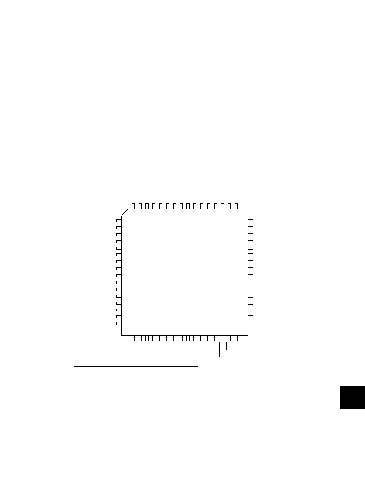
MC68HC05X16
Rev. 1
MOTOROLA
13-1
MECHANICAL DATA
13
13
MECHANICAL DATA
13.1
64-pin quad flat pack (QFP) pinout
Figure 13-1 64-pin QFP pinout
NC
PB0
NW
OI
VPP1
17
18
20
21
22
23
24
25
26
27
29
30
31
32
19
48
47
45
44
43
42
41
40
39
38
37
36
35
34
33
46
PB6
PB7
TX0
PA0
PA1
PA2
PA3
PA4
PA5
PA6
PA7
MDS
TCAP2
TCAP1
PLMB D/A
TX1
PC1
PC0
VSS1
RX0
RX1
VDD1
RDI
SCLK
TDO
TCMP2
TCMP1
PD7/AN7
PD6/AN6
PD5/AN5
NU
VDDH
VRL
VRH
VDD
PD3/AN3
PD2/AN2
PD1/AN1
NU
NC/
CANE
NC/
VPP6
OSC1
OSC2
RESET
IRQ
PLMA D/A
PD4/AN4
PC2/ECLK
PC3
PC5
PC6
PC7
VSS
PB1
PB2
PB3
PB4
PB5
PC4
1
2
4
5
6
7
8
9
10
11
12
13
14
15
16
3
PD0/AN0
28
64
63
61
60
59
58
56
55
54
53
52
51
50
49
62
57
Device
Pin 26
Pin 27
MC68HC05X16, MC68HC05X32
NC
NC
MC68HC705X32
CANE
VPP6
NC = Not connected
NU = Non-user pin (Should be tied to V
SS
in
an electrically noisy environment)
Note:
Unless otherwise stated, a pin labelled as `NU' should be tied to V
SS
in an electrically noisy
environment. Pins labelled `NC' can be left floating, since they are not bonded to any part of the
device.
167

MOTOROLA
13-2
MC68HC05X16
Rev. 1
MECHANICAL DATA
13
13.2
64-pin quad flat pack (QFP) mechanical dimensions
Figure 13-2 64-pin QFP mechanical dimensions
64 lead QFP
0.20 M C A ≠ B S D S
L
33
48
16
1
32
17
49
64
- B -
B
V
0.05 A ≠ B
- D -
A
S
0.20 M H A ≠ B S D S
L
- A -
Detail "A"
B
B
- A, B, D -
P
Detail "A"
F
N
J
D
Section B≠B
Base
Metal
G
H
E
C
-C-
M
Detail "C"
M
-H-
Datum
Plane
Seating
Plane
U
T
R
Q
K
W
X
Dim.
Min.
Max.
Notes
Dim.
Min.
Max.
A
13.90
14.10
1. Datum Plane ≠H≠ is located at bottom of lead and is coincident with
the lead where the lead exits the plastic body at the bottom of the
parting line.
2. Datums A≠B and ≠D to be determined at Datum Plane ≠H≠.
3. Dimensions S and V to be determined at seating plane ≠C≠.
4. Dimensions A and B do not include mould protrusion. Allowable
mould protrusion is 0.25mm per side. Dimensions A and B do
include mould mismatch and are determined at Datum Plane ≠H≠.
5. Dimension D does not include dambar protrusion. Allowable
dambar protrusion shall be 0.08 total in excess of the D dimension
at maximum material condition. Dambar cannot be located on the
lower radius or the foot.
6. Dimensions and tolerancing per ANSI Y 14.5M, 1982.
7. All dimensions in mm.
M
5
∞
10
∞
B
13.90
14.10
N
0.130
0.170
C
2.067
2.457
P
0.40 BSC
D
0.30
0.45
Q
2
∞
8
∞
E
2.00
2.40
R
0.13
0.30
F
0.30
--
S
16.20
16.60
G
0.80 BSC
T
0.20 REF
H
0.067
0.250
U
9
∞
15
∞
J
0.130
0.230
V
16.20
16.60
K
0.50
0.66
W
0.042 NOM
L
12.00 REF
X
1.10
1.30
0.20
M
C
A
≠ B
S
D
S
0.05
A ≠ B
0.20
M
H
A
≠ B
S
D
S
0.20 M C A ≠ B S D S
Case No. 840C
168

MC68HC05X16
Rev. 1
MOTOROLA
14-1
ORDERING INFORMATION
14
14
ORDERING INFORMATION
This section describes the information needed to order the MC68HC05X16 and other family members.
To initiate a ROM pattern for the MCU, you should contact your local field service office, local sales
person or Motorola representative. Please note that you will need to supply details such as: mask
option selections; temperature range; oscillator frequency; package type; electrical test
requirements; and device marking details so that an order can be processed, and a customer
specific part number allocated. Refer to
Table 14-1
for appropriate part numbers. The part number
consists of the device title plus the appropriate suffix. For example, the MC68HC05X16 in 64-pin
QFP package at ≠40 to +85
∞
C would be ordered as: MC68HC05X16CFU.
Note:
The high speed version of the MC68HC05X32 has the same device title as the standard
version. High speed operation is selected via a check box on the order form and will be
confirmed on the listing verification form. See
Appendix C
for electrical characteristics.
Table 14-1 MC order numbers
Device Title
Package Type
Suffix
0 to 70
∞
C
Suffix
-40 to +85
∞
C
Suffix
-40 to +105
∞
C
Suffix
-40 to +125
∞
C
MC68HC05X16
64-pin QFP
FU
CFU
VFU
MFU
MC68HC05X32
64-pin QFP
FU
CFU
VFU
MFU
MC68HC705X32
64-pin QFP
FU
CFU
Contact sales
Contact sales
169

MOTOROLA
14-2
MC68HC05X16
Rev. 1
ORDERING INFORMATION
14
14.1
EPROMS
For the MC68HC05X16, a 16K byte EPROM programmed with the customer's software (positive
logic for address and data) should be submitted for pattern generation. All unused bytes should be
programmed to $00. The size of EPROM which should be used for all other family members is
listed in
Table 14-2
.
The EPROM should be clearly labelled, placed in a conductive IC carrier and securely packed.
14.2
Verification media
All original pattern media (EPROMs) are filed for contractual purposes and are not returned. A
computer listing of the ROM code will be generated and returned with a listing verification form.
The listing should be thoroughly checked and the verification form completed, signed and returned
to Motorola. The signed verification form constitutes the contractual agreement for creation of the
custom mask. If desired, Motorola will program blank EPROMs (supplied by the customer) from
the data file used to create the custom mask, to aid in the verification process.
14.3
ROM verification units (RVU)
Ten MCUs containing the customer's ROM pattern will be provided for program verification. These
units will have been made using the custom mask but are for ROM verification only. For
expediency, they are usually unmarked and are tested only at room temperature (25
∞
C) and at
5 Volts. These RVUs are included in the mask charge and are not production parts. They are
neither backed nor guaranteed by Motorola Quality Assurance.
Table 14-2 EPROMs for pattern generation
Device
Size of EPROM
MC68HC05X16
16K byte
MC68HC05X32
32K byte
170

MC68HC05X16
Rev. 1
MOTOROLA
A-1
MC68HC05X32
15
A
MC68HC05X32
The MC68HC05X32 is a device similar to the MC68HC05X16, but with increased RAM and ROM
sizes. The entire MC68HC05X16 data sheet applies to the MC68HC05X32, with the exceptions
outlined in this appendix.
A.1
Features
∑
31232 bytes of user ROM plus 16 bytes of user vectors
∑
528 bytes of RAM
∑
654 bytes of bootstrap ROM
∑
Available in 64-pin QFP package
∑
High speed operation (4 MHz bus speed) available. See
Appendix C
for tables of electrical
characteristics.
∑
≠ 40
∞
to +125
∞
C temperature range
Important note
The following applies to the D53J MC68HC05X32 mask set only:
≠
Mask options on the MC68HC05X32 allow the customer to
select POR delay cycles and oscillator DIV ratio. However,
during reset, options of 4064 cycles POR and DIV 10 are
forced, regardless of which options the customer has selected.
Therefore, a power-on reset delay of 40640 oscillator cycles is
forced.
On the D53J mask set, DIV10 is forced in bootstrap mode. On later mask set
revisions, including D69J, DIV2 is forced in bootstrap mode.
171

MOTOROLA
A-2
MC68HC05X16
Rev. 1
MC68HC05X32
15
Note:
The electrical characteristics for the MC68HC05X16 should not be used for the
MC68HC05X32.
Section A.3.1
to
Section A.3.4
contain data specific to this device.
A.2
Memory map, register outline and block diagram
Figure A-1 MC68HC05X32 block diagram
Po
r
t
A
PA0
PA1
PA2
PA3
PA4
PA5
PA6
PA7
Po
r
t
B
PB0
PB1
PB2
PB3
PB4
PB5
PB6
PB7
Po
r
t
C
PC0
PC1
PC2/ECLK
PC3
PC4
PC5
PC6
PC7
16-bit
programmable
timer
Po
r
t
D
PD0/AN0
PD1/AN1
PD2/AN2
PD3/AN3
PD4/AN4
PD5/AN5
PD6/AN6
PD7/AN7
Oscillator
528 bytes
RAM
COP watchdog
RESET
IRQ
VDD
VSS
OSC1
OSC2
M68HC05
CPU
SCI
A/D converter
PLM
TCAP1
TCAP2
TCMP1
TCMP2
VRH
VRL
RDI
SCLK
TDO
VPP1
256 bytes
EEPROM
Charge pump
˜
2 /
˜
32
PLMA D/A
PLMB D/A
8-bit
654 bytes
user ROM
31248 bytes
bootstrap
ROM
(including 16 bytes
user vectors)
Line
interface
MCAN
VDDH
TX0
TX1
RX0
RX1
VDD1
VSS1
MDS
NWOI
172
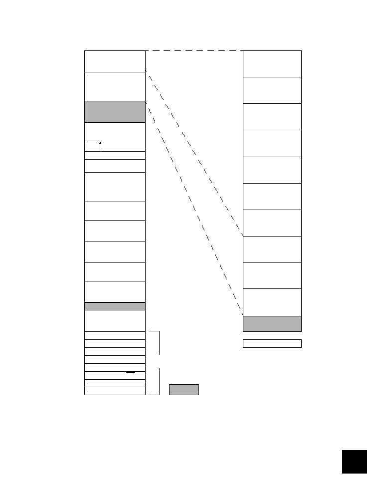
MC68HC05X16
Rev. 1
MOTOROLA
A-3
MC68HC05X32
15
Figure A-2 Memory map of the MC68HC05X32
User
Vectors
Reserved
I/O and registers
(32 bytes)
Stack
RAM I
(176 bytes)
Bootstrap ROM I
(80 bytes)
User ROM
(31232 bytes)
Bootstrap ROM II
(80 bytes)
OPTR (1 byte)
Non protected (31 bytes)
Protected (224 bytes)
EEPROM
(256 bytes)
MC68HC05X32
SCI
Timer overflow
Timer output compare 1& 2
Timer input capture 1& 2
WOI, External IRQ
SWI
Reset/power-on reset
RAM II
352 bytes
MCAN
registers
CIRQ
MCAN
control registers
10 bytes
MCAN
transmit buffer
10 bytes
MCAN
receive buffer
10 bytes
Ports
7 bytes
EEPROM/ECLK
control
1 byte
PLM system
2 bytes
A/D
converter
2 bytes
Miscellaneous
1 byte
SCI
5 bytes
Timer
14 bytes
(30 bytes)
Bootstrap ROM III
(478 bytes)
Bootstrap ROM vectors
(16 bytes)
$0100
Options register
Register
$7FFE≠F
$7FF6≠7
$0000
$0020
$0050
$7FF0≠1
$0120
$0101
$0250
$003E
$0200
$7FF2≠3
$00C0
$0100
$7FF4≠5
$7FF8≠9
$7FFA≠B
$7FFC≠D
$03B0
$0400
$7E00
$7FDE
$7FE0
$0000
$0007
$0008
$000A
$000C
$000D
$0012
$0020
$002A
$0034
$003E
$0047
173

MOTOROLA
A-4
MC68HC05X16
Rev. 1
MC68HC05X32
15
Figure A-2 Memory map of the MC68HC05X32 (Continued)
Port B data register
Port C data register
Port D input data register
Port A data register
$0000
Compare low register 2
A/D data register
Port A data direction register
Port B data direction register
Port C data direction register
E/EEPROM/ECLK control register
A/D status/control register
Pulse length modulation A
Pulse length modulation B
Miscellaneous register
SCI baud rate register
SCI control register 1
SCI control register 2
SCI status register
SCI data register
Timer control register
Timer status register
Capture high register 1
Capture low register 1
Compare high register 1
Compare low register 1
Counter high register
Counter low register
Alternate counter high register
Alternate counter low register
Capture high register 2
Capture low register 2
Compare high register 2
$0001
$0002
$0003
$0004
$0005
$0006
$0007
$0008
$0009
$000A
$000B
$000C
$000D
$000E
$000F
$0010
$0011
$0012
$0013
$0014
$0015
$0016
$0017
$0018
$0019
$001A
$001B
$001C
$001D
$001E
$001F
Receive data field (8 bytes)
Control register
Command register
Status register
Interrupt register
Acceptance code register
Acceptance mask register
Bus timing register 0
Bus timing register 1
Output control register
Test register
Transmit identifier
ATR bit/data length code
Transmit data field (8 bytes)
Receive identifier
ATR bit/data length code
$0020
$0021
$0022
$0023
$0024
$0025
$0026
$0027
$0028
$0029
$002A
$002B
$002C
$0034
$0035
$0036
$003D
Registe
MCAN
control registers
10 bytes
MCAN
transmit buffer
10 bytes
MCAN
receive buffer
10 bytes
Ports
7 bytes
EEPROM/ECLK
control
1 byte
PLM system
2 bytes
A/D
converter
2 bytes
Miscellaneous
1 byte
SCI
5 bytes
Timer
14 bytes
$0100
Options register
$0047
Register
$0000
$0007
$0008
$000A
$000C
$000D
$0012
$0020
$002A
$0034
$003E
174

MC68HC05X16
Rev. 1
MOTOROLA
A-5
MC68HC05X32
15
(1) This bit is set each time there is a power-on reset.
(2) The state of the WDOG bit after reset is dependent upon the mask option selected; 1 = watchdog enabled, 0 = watchdog disabled.
(3) This register is implemented in EEPROM; therefore reset has no effect on the individual bits.
Table A-1 Register outline
Register name
Address
bit 7
bit 6
bit 5
bit 4
bit 3
bit 2
bit 1
bit 0
State on
reset
Port A data (PORTA)
$0000
Undefined
Port B data (PORTB)
$0001
Undefined
Port C data (PORTC)
$0002
PC2/
ECLK
Undefined
Port D data (PORTD)
$0003
PD7
PD6
PD5
PD4
PD3
PD2
PD1
PD0
Undefined
Port A data direction (DDRA)
$0004
0000 0000
Port B data direction (DDRB)
$0005
0000 0000
Port C data direction (DDRC)
$0006
0000 0000
EEPROM/ECLK control
$0007
WOIE
CAF
0
0
ECLK
E1ERA E1LAT E1PGM
0000 0000
A/D data (ADDATA)
$0008
0000 0000
A/D status/control (ADSTAT)
$0009
COCO ADRC ADON
0
CH3
CH2
CH1
CH0
0000 0000
Pulse length modulation A (PLMA) $000A
0000 0000
Pulse length modulation B (PLMB) $000B
0000 0000
Miscellaneous
$000C
POR
(1)
INTP
INTN
INTE
SFA
SFB
SM
WDOG
(2)
u001 000u
SCI baud rate (BAUD)
$000D
SPC1
SPC0
SCT1
SCT0
SCT0
SCR2
SCR1
SCR0
00uu uuuu
SCI control 1 (SCCR1)
$000E
R8
T8
M
WAKE
CPOL
CPHA
LBCL
Undefined
SCI control 2 (SCCR2)
$000F
TIE
TCIE
RIE
ILIE
TE
RE
RWU
SBK
0000 0000
SCI status (SCSR)
$0010
TDRE
TC
RDRF
IDLE
OR
NF
FE
1100 000u
SCI data (SCDR)
$0011
0000 0000
Timer control (TCR)
$0012
ICIE
OCIE
TOIE
FOLV2 FOLV1
OLV2
IEDG1 OLVL1
0000 00u0
Timer status (TSR)
$0013
ICF1
OCF1
TOF
ICF2
OCF2
Undefined
Input capture high 1
$0014
Undefined
Input capture low 1
$0015
Undefined
Output compare high 1
$0016
Undefined
Output compare low 1
$0017
Undefined
Timer counter high
$0018
1111 1111
Timer counter low
$0019
1111 1100
Alternate counter high
$001A
1111 1111
Alternate counter low
$001B
1111 1100
Input capture high 2
$001C
Undefined
Input capture low 2
$001D
Undefined
Output compare high 2
$001E
Undefined
Output compare low 2
$001F
Undefined
Options (OPTR)
(3)
$0100
EE1P
SEC
Not affected
175

MOTOROLA
A-6
MC68HC05X16
Rev. 1
MC68HC05X32
15
A.3
Electrical specifications
This section contains the electrical specifications and associated timing information for the
MC68HC05X32.
A.3.1
Maximum ratings
Note:
This device contains circuitry designed to protect against damage due to high
electrostatic voltages or electric fields. However, it is recommended that normal
precautions be taken to avoid the application of any voltages higher than those given in
the maximum ratings table to this high impedance circuit. For maximum reliability all
unused inputs should be tied to either V
SS
or V
DD
.
(1) All voltages are with respect to V
SS
.
(2) Maximum current drain per pin is for one pin at a time, limited by an external resistor.
Table A-2 Maximum ratings
Rating
Symbol
Value
Unit
Supply voltage
(1)
V
DD
≠ 0.5 to +7.0
V
Input voltage
V
IN
V
SS
≠ 0.5 to V
DD
+ 0.5
V
Input voltage
≠ bootstrap mode (IRQ pin only)
V
IN
V
SS
≠ 0.5 to 2V
DD
+ 0.5
V
Operating temperature range
T
A
T
L
to T
H
≠ 40 to +125
∞
C
Storage temperature range
T
STG
≠ 65 to +150
∞
C
Current drain per pin
(2)
(Excluding VDD, VSS, VDD1 and VSS1)
≠ Source
≠ Sink
I
D
I
S
25
45
mA
mA
External oscillator frequency
f
OSC
22
MHz
176

MC68HC05X16
Rev. 1
MOTOROLA
A-7
MC68HC05X32
15
A.3.2
DC electrical characteristics
Table A-3 DC electrical characteristics
(
V
DD
= 5.0 Vdc
±
10%, V
SS
= 0 Vdc, T
A
= ≠40
∞
C to +125
∞
C)
Characteristic
(1)
Symbol
Min
Typ
(2)
Max
Unit
Output voltage
I
LOAD
= ≠ 10
µ
A
I
LOAD
= +10
µ
A
V
OH
V
OL
V
DD
≠ 0.1
--
--
--
--
0.1
V
Output high voltage (I
LOAD
= 0.8mA)
PA0≠7, PB0≠7, PC0≠7, TCMP1, TCMP2,
Output high voltage (I
LOAD
= 1.6mA)
TDO, SCLK, PLMA, PLMB
Output high voltage (I
LOAD
= ≠300
µ
A)
OSC2
V
OH
V
OH
V
OH
V
DD
≠ 0.8
V
DD
≠ 0.8
V
DD
≠ 0.8
V
DD
≠ 0.2
V
DD
≠ 0.2
V
DD
≠ 0.3
--
--
--
V
Output low voltage (I
LOAD
= 1.6mA)
PA0≠7, PB0≠7, PC0≠7, TCMP1, TCMP2,
TDO, SCLK, PLMA, PLMB
Output low voltage (I
LOAD
= 1.6mA)
RESET
Output low voltage (I
LOAD
= ≠100
µ
A)
OSC2
V
OL
V
OL
V
OL
--
--
--
0.1
0.2
0.2
0.4
0.6
0.4
V
Input high voltage
PA0≠7, PB0≠7, PC0≠7, PD0≠7, OSC1, IRQ,
RESET, TCAP1, TCAP2, RDI, MDS, NWOI
V
IH
0.7 V
DD
--
V
DD
V
Input low voltage
PA0≠7, PB0≠7, PC0≠7, PD0≠7, OSC1, IRQ,
RESET, TCAP1, TCAP2, RDI, MDS, NWOI
V
IL
V
SS
--
0.2V
DD
V
Can comparator I
DD
(I
DD1
)
(3)(4)(5)
Supply current in DIV2 mode
RUN: CAN active
(6)
STOP: CAN active
WAIT: CAN asleep
(7)
STOP: CAN asleep
I
DD1
I
DD1
I
DD1
I
DD1
--
--
--
--
360
360
32
10
900
900
100
30
µ
A
µ
A
µ
A
µ
A
MCU I
DD
(3)(4)(8)
Supply current in DIV 2 mode
RUN (SM = 0): CAN active
RUN (SM = 1): CAN active
WAIT (SM = 0): CAN active
WAIT (SM =1): CAN active
WAIT (SM = 0): CAN asleep
WAIT (SM = 1): CAN asleep
STOP: CAN active
STOP: CAN asleep
I
DD
I
DD
I
DD
I
DD
I
DD
I
DD
I
DD
I
DD
--
--
--
--
--
--
--
--
3.6
1.6
1.8
1.5
0.8
0.4
0.5
90
7
3.6
4
3.7
1.4
1.1
1.5
300
mA
mA
mA
mA
mA
mA
mA
µ
A
MCU I
DD
(3)(5)(8)
Supply current in DIV 10 mode
RUN (SM = 0): CAN active
RUN (SM = 1): CAN active
WAIT (SM = 0): CAN active
WAIT (SM =1): CAN active
WAIT (SM = 0): CAN asleep
WAIT (SM = 1): CAN asleep
STOP: CAN active
STOP: CAN asleep
I
DD
I
DD
I
DD
I
DD
I
DD
I
DD
I
DD
I
DD
--
--
--
--
--
--
--
--
6.6
4.6
4.6
4.5
1.2
0.8
0.5
90
13
8
8.5
8
1.8
1.4
1.5
300
mA
mA
mA
mA
mA
mA
mA
µ
A
High-Z leakage current
PA0≠7, PB0≠7, PC0≠7, TDO, RESET, SCLK
I
IL
--
±
0.2
±
1
µ
A
177

MOTOROLA
A-8
MC68HC05X16
Rev. 1
MC68HC05X32
15
(1) All I
DD
measurements taken with suitable decoupling capacitors across the power supply to suppress the transient
switching currents inherent in CMOS designs (see Section 2).
(2) Typical values are at mid point of voltage range and at 25
∞
C only.
(3) RUN and WAIT I
DD
: measured using an external square-wave clock source, refer to
Figure 2-6
(c); all inputs 0.2 V
from rail; no DC loads; maximum load on outputs 50pF (20pF on OSC2).
STOP/WAIT I
DD
: all ports configured as inputs; V
IL
= 0.2 V and V
IH
= V
DD
≠ 0.2 V: STOP I
DD
measured with
OSC1 = V
DD
. WAIT I
DD
is affected linearly by the OSC2 capacitance.
(4) f
OSC
= 4.4 MHz; f
BUS
= 2.2 MHz; f
CAN
= 2.2 MHz
(5) f
OSC
= 22 MHz; f
BUS
= 2.2 MHz; f
CAN
= 11 MHz
(6) These limits are also applicable under the following conditions:
MCU RUN mode/SLOW mode/CAN active
MCU WAIT mode/SLOW mode/CAN active
MCU WAIT mode/CAN active
(7) These limits are also applicable under the following conditions:
MCU WAIT mode/SLOW mode/CAN asleep
(8) These currents are the summation of the MCU current + CAN current (I
DD
+ I
DD1
)
(9) Current injection is guaranteed but not tested.
Functionality of the MCU is guaranteed during injection of dc current up to the maximum specified level.
The maximum specified current for each port is the sum of the magnitudes of the currents on each side of the
individual port pins.
Some disturbance of the A/D accuracy is possible during an injection event and is dependent on board layout,
power supply decoupling and reference voltage decoupling configurations.
Input current
OSC1=V
DD
(OSC2=V
SS
)
Input current
OSC1=V
SS
(OSC2=V
DD
)
I
FH
I
FL
≠10
--
--
--
--
+10
µ
A
Input current
IRQ, TCAP1, TCAP2, RDI,
PD0/AN0-PD7/AN7 (channel not selected)
I
IN
--
±
0.2
±
1
µ
A
Capacitance
Ports (as input or output), RESET, TDO, SCLK
IRQ, TCAP1, TCAP2, OSC1, RDI
PD0/AN0≠PD7/AN7 (A/D off)
PD0/AN0≠PD7/AN7 (A/D on)
C
OUT
C
IN
C
IN
C
IN
--
--
--
--
--
--
12
22
12
8
--
--
pF
pF
pF
pF
DC injection current
(9)
Port A (PA0≠PA7)
Port B (PB0≠PB7)
|I
INJ
|
|I
INJ
|
--
--
--
--
10
10
mA
mA
Table A-3 DC electrical characteristics
(
V
DD
= 5.0 Vdc
±
10%, V
SS
= 0 Vdc, T
A
= ≠40
∞
C to +125
∞
C)
Characteristic
(1)
Symbol
Min
Typ
(2)
Max
Unit
178

MC68HC05X16
Rev. 1
MOTOROLA
A-9
MC68HC05X32
15
A.3.3
A/D converter characteristics
(1) Performance verified down to 2.5V
VR, but accuracy is tested and guaranteed at
VR = 5V
±
10%.
(2) Source impedances greater than 10k
will adversely affect internal charging time during input sampling.
(3) The external system error caused by input leakage current is approximately equal to the product of R source and input
current. Input current to A/D channel will be dependent on external source impedance (see
Figure 9-2
).
Table A-4 A/D characteristics
(V
DD
= 5.0 Vdc
±
10%, V
SS
= 0 Vdc, T
A
= ≠40
∞
C to +125
∞
C)
Characteristic
Parameter
Min
Max
Unit
Resolution
Number of bits resolved by the A/D
8
--
Bit
Non-linearity
Max deviation from the best straight line through the A/D
transfer characteristics
(V
RH
= V
DD
and V
RL
= 0V)
--
±
0.5
LSB
Quantization error
Uncertainty due to converter resolution
--
±
0.5
LSB
Absolute accuracy
Difference between the actual input voltage and the
full-scale equivalent of the binary code output code for all
errors
--
±
1
LSB
Conversion range
Analog input voltage range
V
RL
V
RH
V
V
RH
Maximum analog reference voltage
V
RL
V
DD
+ 0.1
V
V
RL
Minimum analog reference voltage
V
SS
≠ 0.1
V
RH
V
V
R
(1)
Minimum difference between V
RH
and V
RL
3
--
V
Conversion time
Total time to perform a single analog to digital conversion
a. External clock (OSC1, OSC2)
b. Internal RC oscillator
--
--
32
32
t
CYC
µ
s
Monotonicity
Conversion result never decreases with an increase in
input voltage and has no missing codes
GUARANTEED
Zero input reading
Conversion result when V
IN
= V
RL
00
--
Hex
Full scale reading
Conversion result when V
IN
= V
RH
--
FF
Hex
Sample acquisition time
Analog input acquisition sampling
a. External clock (OSC1, OSC2)
b. Internal RC oscillator
(2)
--
--
12
12
t
CYC
µ
s
Sample/hold capacitance Input capacitance on PD0/AN0≠PD7/AN7
--
12
pF
Input leakage
(3)
Input leakage on A/D pins PD0/AN0≠PD7/AN7, VRL, VRH
--
1
µ
A
179

MOTOROLA
A-10
MC68HC05X16
Rev. 1
MC68HC05X32
15
A.3.4
Control timing
(1) For bus frequencies less than 2 MHz, the internal RC oscillator should be used when
programming the EEPROM.
(2) Since a 2-bit prescaler in the timer must count four external cycles (t
cyc
), this is the limiting
factor in determining the timer resolution.
(3) The minimum period t
TLTL
should not be less than the number of cycle times it takes to execute
the capture interrupt service routine plus 24 t
cyc
.
(4) The minimum period t
ILIL
should not be less than the number of cycle times it takes to execute
the interrupt service routine plus 21 t
cyc
.
(5) At a temperature of 85
∞
C.
(6) Refer to Reliability Monitor Report (currrent quarterly issue) for current failure rate information.
Table A-5 Control timing
(V
DD
= 5.0 Vdc
±
10%, V
SS
= 0 Vdc, T
A
= ≠40
∞
C to +125
∞
C)
Characteristic
Symbol
Min
Max
Unit
Frequency of operation
Oscillator frequency
MCAN module clock frequency
MCU bus frequency
f
OSC
f
CAN
f
MCU
0
0
0
22
11
2.2
MHz
MHz
MHz
Cycle time (see
Figure 10-1
)
t
CYC
455
--
ns
Crystal oscillator start-up time (see
Figure 10-1
)
t
OXOV
--
100
ms
Stop recovery start-up time (crystal oscillator)
t
ILCH
100
ms
A/D converter stabilization time
t
ADON
500
µ
s
External RESET input pulse width
t
RL
1.5
--
t
CYC
Power-on RESET output pulse width (mask option)
4064 cycle
16 cycle
t
PORL
t
PORL
4064
16
--
--
t
CYC
t
CYC
Watchdog RESET output pulse width
t
DOGL
1.5
--
t
CYC
Watchdog time-out
t
DOG
6144
7168
t
CYC
EEPROM byte erase time
t
ERA
10
10
ms
EEPROM byte program time
(1)
t
PROG
10
10
ms
Timer (see
Figure A-3
)
Resolution
(2)
Input capture pulse width
Input capture pulse period
t
RESL
t
TH
, t
TL
t
TLTL
4
125
--
(3)
--
--
--
t
CYC
ns
t
CYC
Interrupt pulse width (edge-triggered)
t
ILIH
125
--
ns
Interrupt pulse period
t
ILIL
--
(4)
--
t
CYC
OSC1 pulse width
t
OH
, t
OL
90
--
ns
Write/erase endurance
(5)(6)
--
10000
cycles
Data retention
(5)(6)
--
10
years
180

MC68HC05X16
Rev. 1
MOTOROLA
A-11
MC68HC05X32
15
A.3.5
MCAN bus interface DC electrical characteristics
(1) Maximum DC current should comply with maximum ratings.
Figure A-3 Timer relationship
Table 1-6 MCAN bus interface DC electrical characteristics
(V
DD
= 5.0 Vdc
±
10%, V
SS
= 0 Vdc, T
A
= ≠40
∞
C to +125
∞
C)
Characteristic
Symbol
Min
Max
Unit
MCAN bus input comparator: pins RX0 and RX1
Input voltage
Common mode range
Latch-up trigger current
(1)
Input offset voltage
Hysteresis
V
IN
C
MR
I
LT
V
OFS
V
HYS
0.5
1.5
≠100
≠30
1
V
DD
+0.5
V
DD
≠1.5
+100
+30
22
V
V
mA
mV
mV
V
DD
˜
2 generator: pin VDDH
Output voltage difference to V
DD
˜
2 for
≠100
µ
A < I
OUT
< +100
µ
A
Output current
Latch-up trigger current
(1)
DV
OUT
I
OUT
I
LT
≠200
≠100
≠100
+200
+100
+100
mV
mA
mA
MCAN bus output driver: pins TX0 and TX1
Source current per pin (V
OUT
= V
DD
≠1.0V)
Sink current per pin (V
OUT
= 1.0V)
Latch-up trigger current
(1)
I
OH
I
OL
I
LT
≠10
10
≠100
--
--
+100
mA
mA
mA
(V
DD
= 5.0 Vdc
±
2%, V
SS
= 0 Vdc, T
A
= ≠40
∞
C to +125
∞
C)
Characteristic
Symbol
Min
Max
Unit
V
DD
˜
2 generator: pin VDDH
Output voltage difference to V
DD
˜
2 for
≠100
µ
A < I
OUT
< +100
µ
A
DV
OUT
≠180
+180
mV
External
signal
(TCAP1,
TCAP2)
t
TLTL
t
TH
t
TL
181

MOTOROLA
A-12
MC68HC05X16
Rev. 1
MC68HC05X32
15
A.3.6
MCAN bus interface control timing characteristics
Table 1-7 MCAN bus interface control timing characteristics
(4.5V
V
DD
5.5V, V
SS
= 0 Vdc, T
A
= ≠40
∞
C to +125
∞
C)
Characteristic
Symbol
Min
Max
Unit
MCAN bus output driver
Rise and fall time (C
LOAD
= 100pF)
T
RF
--
25
ns
182

MC68HC05X16
Rev. 1
MOTOROLA
B-1
MC68HC705X32
15
B
MC68HC705X32
The MC68HC705X32 is a device similar to the MC68HC05X16, but with 32K bytes of EPROM
instead of 16K bytes of ROM. In addition, the bootstrap routines available in the MC68HC05X16
are replaced by bootstrap routines specific to the MC68HC705X32. The entire MC68HC05X16
data sheet applies to the MC68HC705X32, with the exceptions outlined in this appendix.
Important note
The following applies to the D59J MC68HC705X32 mask set only.
≠
A mask option register (MOR) on the MC68HC705X32 allows
the customer to select POR delay cycles and oscillator DIV
ratio. However, during reset, options of 4064 cycles POR and
DIV10 are forced, regardless of which options the customer has
selected. Therefore, a power-on reset delay of 40640 oscillator
cycles is forced.
On the D59J mask set, the oscillator divide ratio depends on the CANE pin:
CANE = 1
DIV10 forced in bootloader mode
CANE = 0
DIV2 forced in bootloader mode
On later mask set revisions, including G47V, DIV2 is forced in bootloader mode,
regardless of the CANE pin.
The following applies to the D40J and D59J MC68HC705X32 mask sets only:
≠
The minimum external RESET input pulse width, t
RL
(
Table B-10
) is 1.5 t
CYC
≠
Maximum bus speed 2.2 MHz
183

MOTOROLA
B-2
MC68HC05X16
Rev. 1
MC68HC705X32
15
B.1
Features
∑
≠40 to +125
∞
C operating temperature range
∑
31232 bytes user EPROM plus 16 bytes of EPROM user vectors
∑
528 bytes of RAM
∑
654 bytes bootstrap ROM
∑
Simultaneous programming of up to 16 bytes of EPROM
∑
4 MHz bus speed
∑
Available in 64-pin QFP package
Note:
The electrical characteristics for the MC68HC05X16 should not be used for the
MC68HC705X32.
Section B.9.2
and
Section B.9.5
contain data specific to this device.
B.2
VPP6
The VPP6 pin is the voltage input for the EPROM in both read and programming modes (see
Section B.5
).
B.3
CANE
This pin is the MCAN enable input. If CANE is connected to VDD, the internal MCAN module is
selected and its registers are mapped at addresses $0020 to $003D.
Note:
Although this pin can be left floating to disconnect the MCAN module, it is advisable to
connect it to VSS when the module is not in use.
184

MC68HC05X16
Rev. 1
MOTOROLA
B-3
MC68HC705X32
15
B.4
Block diagram, memory map and register outline
Figure B-1 MC68HC705X32 block diagram
Po
r
t
A
PA0
PA1
PA2
PA3
PA4
PA5
PA6
PA7
Po
r
t
B
PB0
PB1
PB2
PB3
PB4
PB5
PB6
PB7
Po
r
t
C
PC0
PC1
PC2/ECLK
PC3
PC4
PC5
PC6
PC7
16-bit
programmable
timer
Po
r
t
D
PD0/AN0
PD1/AN1
PD2/AN2
PD3/AN3
PD4/AN4
PD5/AN5
PD6/AN6
PD7/AN7
Oscillator
528 bytes
RAM
COP watchdog
RESET
IRQ
VDD
VSS
OSC1
OSC2
M68HC05
CPU
SCI
A/D converter
PLM
TCAP1
TCAP2
TCMP1
TCMP2
VRH
VRL
RDI
SCLK
TDO
VPP1
256 bytes
EEPROM
Charge pump
˜
2 /
˜
32
PLMA D/A
PLMB D/A
8-bit
654 bytes
EPROM
31248 bytes
bootstrap ROM
(including 16 bytes
user vectors)
Line
interface
MCAN
VDDH
TX0
TX1
RX0
RX1
VDD1
VSS1
CANE
MDS
VPP6
NWOI
185
MOTOROLA
B-4
MC68HC05X16
Rev. 1
MC68HC705X32
15
(1) This bit is set each time there is a power-on reset.
(2) The state of the WDOG bit after reset is dependent upon the mask option selected; 1 = watchdog enabled, 0 = watchdog disabled.
(3) This register is implemented in EEPROM; therefore reset has no effect on the individual bits.
(4) This register is implemented in EPROM; therefore reset has no effect on the individual bits. However, please read the important note on page
B-1.
Table B-1 Register outline
Register name
Address bit 7
bit 6
bit 5
bit 4
bit 3
bit 2
bit 1
bit 0
State on
reset
Port A data (PORTA)
$0000
Undefined
Port B data (PORTB)
$0001
Undefined
Port C data (PORTC)
$0002
PC2/ECLK
Undefined
Port D data (PORTD)
$0003
PD7
PD6
PD5
PD4
PD3
PD2
PD1
PD0
Undefined
Port A data direction (DDRA)
$0004
0000 0000
Port B data direction (DDRB)
$0005
0000 0000
Port C data direction (DDRC)
$0006
0000 0000
EEPROM/ECLK control
$0007
WOIE
CAF
E6LAT E6PGM ECLK
E1ERA E1LAT E1PGM 0000 0000
A/D data (ADDATA)
$0008
0000 0000
A/D status/control (ADSTAT)
$0009
COCO ADRC ADON
0
CH3
CH2
CH1
CH0
0000 0000
Pulse length modulation A (PLMA) $000A
0000 0000
Pulse length modulation B (PLMB) $000B
0000 0000
Miscellaneous
$000C POR
(1)
INTP
INTN
INTE
SFA
SFB
SM
WDOG
(2)
u001 000u
SCI baud rate (BAUD)
$000D
SPC1
SPC0
SCT1
SCT0
SCT0
SCR2
SCR1
SCR0
00uu uuuu
SCI control 1 (SCCR1)
$000E
R8
T8
M
WAKE
CPOL
CPHA
LBCL
Undefined
SCI control 2 (SCCR2)
$000F
TIE
TCIE
RIE
ILIE
TE
RE
RWU
SBK
0000 0000
SCI status (SCSR)
$0010
TDRE
TC
RDRF
IDLE
OR
NF
FE
1100 000u
SCI data (SCDR)
$0011
0000 0000
Timer control (TCR)
$0012
ICIE
OCIE
TOIE
FOLV2 FOLV1
OLV2
IEDG1 OLVL1 0000 00u0
Timer status (TSR)
$0013
ICF1
OCF1
TOF
ICF2
OCF2
Undefined
Input capture high 1
$0014
Undefined
Input capture low 1
$0015
Undefined
Output compare high 1
$0016
Undefined
Output compare low 1
$0017
Undefined
Timer counter high
$0018
1111 1111
Timer counter low
$0019
1111 1100
Alternate counter high
$001A
1111 1111
Alternate counter low
$001B
1111 1100
Input capture high 2
$001C
Undefined
Input capture low 2
$001D
Undefined
Output compare high 2
$001E
Undefined
Output compare low 2
$001F
Undefined
Options (OPTR)
(3)
$0100
EE1P
SEC
Not affected
Mask option register (MOR)
(4)
$7FDE
WOI
DIV2
DIV8
RTIM
RWAT
WWAT
PBPD
PCPD Not affected
186

MC68HC05X16
Rev. 1
MOTOROLA
B-5
MC68HC705X32
15
Figure B-2 Memory map of the MC68HC705X32
EPROM
User
Reserved
I/O and registers
(32 bytes)
Stack
RAM I
(176 bytes)
Bootstrap ROM I
(80 bytes)
User EPROM
(31232 bytes)
Bootstrap ROM II
(80 bytes)
OPTR (1 byte)
Non protected (31 bytes)
Protected (224 bytes)
EEPROM
(256 bytes)
MC68HC705X32
SCI
Timer overflow
Timer output compare 1& 2
Timer input capture 1& 2
WOI, External IRQ
SWI
Reset/power-on reset
RAM II
352 bytes
MCAN
registers
CIRQ
MCAN
control registers
10 bytes
MCAN
transmit buffer
10 bytes
MCAN
receive buffer
10 bytes
Ports
7 bytes
EEPROM/ECLK
control
1 byte
PLM system
2 bytes
A/D
converter
2 bytes
Miscellaneous
1 byte
SCI
5 bytes
Timer
14 bytes
$7FDE
Mask options register
(30 bytes)
Mask options register
Bootstrap ROM III
(478 bytes)
Bootstrap ROM vectors
(16 bytes)
$0100
Options register
Register groups
$7FFE≠F
$7FF6≠7
$0000
$0020
$0050
$7FF0≠1
$0120
$0101
$0250
$003E
$0200
$7FF2≠3
$00C0
$0100
$7FF4≠5
$7FF8≠9
$7FFA≠B
$7FFC≠D
$03B0
$0400
$7E00
$7FDE
$7FDF
$7FE0
$0000
$0007
$0008
$000A
$000C
$000D
$0012
$0020
$002A
$0034
$003E
$0047
Vectors
187

MOTOROLA
B-6
MC68HC05X16
Rev. 1
MC68HC705X32
15
Figure B-2 Memory map of the MC68HC705X32 (Continued)
Port B data register
Port C data register
Port D input data register
Port A data register
$0000
Compare low register 2
A/D data register
Port A data direction register
Port B data direction register
Port C data direction register
E/EEPROM/ECLK control register
A/D status/control register
Pulse length modulation A
Pulse length modulation B
Miscellaneous register
SCI baud rate register
SCI control register 1
SCI control register 2
SCI status register
SCI data register
Timer control register
Timer status register
Capture high register 1
Capture low register 1
Compare high register 1
Compare low register 1
Counter high register
Counter low register
Alternate counter high register
Alternate counter low register
Capture high register 2
Capture low register 2
Compare high register 2
$0001
$0002
$0003
$0004
$0005
$0006
$0007
$0008
$0009
$000A
$000B
$000C
$000D
$000E
$000F
$0010
$0011
$0012
$0013
$0014
$0015
$0016
$0017
$0018
$0019
$001A
$001B
$001C
$001D
$001E
$001F
Receive data field (8 bytes)
Control register
Command register
Status register
Interrupt register
Acceptance code register
Acceptance mask register
Bus timing register 0
Bus timing register 1
Output control register
Test register
Transmit identifier
ATR bit/data length code
Transmit data field (8 bytes)
Receive identifier
ATR bit/data length code
$0020
$0021
$0022
$0023
$0024
$0025
$0026
$0027
$0028
$0029
$002A
$002B
$002C
$0034
$0035
$0036
$003D
Registers
MCAN
control registers
10 bytes
MCAN
transmit buffer
10 bytes
MCAN
receive buffer
10 bytes
Ports
7 bytes
EEPROM/ECLK
control
1 byte
PLM system
2 bytes
A/D
converter
2 bytes
Miscellaneous
1 byte
SCI
5 bytes
Timer
14 bytes
$7FDE
Mask options register
$0100
Options register
$0047
Register groups
$0000
$0007
$0008
$000A
$000C
$000D
$0012
$0020
$002A
$0034
$003E
188

MC68HC05X16
Rev. 1
MOTOROLA
B-7
MC68HC705X32
15
B.5
EPROM
The MC68HC705X32 memory map is given in
Figure B-2
. The device has a total of 31248 bytes
of EPROM. 16 bytes are used for the reset and interrupt vectors from address $7FF0 to $7FFF.
The main EPROM block of 31232 bytes is located from $0400 to $7DFF. One byte of EPROM is
used as an option register and is located at address $7FDE.
The EPROM can be completely tested before assembly with sequences of both program and
erase. It is finally erased before being typically assembled in a package with no erase window.
Therefore, only programming is possible and the EPROM operates as a PROM.
The EPROM array is supplied by the VPP6 pin in both read and program modes. Typically the
user's software would be loaded into a programming board where V
PP6
is controlled by one of the
bootstrap loader routines. It would then be placed in an application where no programming occurs.
In this case the VPP6 pin should be hardwired to V
DD
.
Warning: A minimum V
PP6R
voltage must be applied to the VPP6 pin at all times, including
power-on. Failure to do so could result in permanent damage to the device. Unless
otherwise stated, EPROM programming is guaranteed at ambient temperature (25
∞
C)
only.
B.5.1
EPROM read operation
The execution of a program in the EPROM address range or a load from the EPROM are both read
operations. The E6LAT bit in the EPROM/EEPROM control register should be cleared to `0' which
automatically resets the E6PGM bit. In this way the EPROM is read like a normal ROM. Reading
the EPROM with the E6LAT bit set will give data that does not correspond to the actual memory
content. As interrupt vectors are in EPROM, they will not be loaded when E6LAT is set. Similarly,
the bootstrap ROM routines cannot be executed when E6LAT is set. In read mode, the VPP6 pin
must be at the V
PP6R
level. When entering the STOP mode, the EPROM is automatically set to the
read mode.
Note:
An erased byte reads as $00.
189

MOTOROLA
B-8
MC68HC05X16
Rev. 1
MC68HC705X32
15
B.5.2
EPROM program operation
Typically the EPROM will be programmed by the bootstrap routines resident in the on-chip ROM.
However, the user program can be used to program some EPROM locations if the proper
procedure is followed. In particular, the programming sequence must be running in RAM, as the
EPROM will not be available for code execution while the E6LAT bit is set. The V
PP6
switching must
occur externally after the E6PGM bit is set, for example under control of a signal generated on a
pin by the programming routine.
Note:
When the part becomes a PROM, only the cumulative programming of bits to logic `1'
is possible if multiple programming is made on the same byte.
To allow simultaneous programming of up to sixteen bytes, these bytes must be in the same group
of addresses which share the same most significant address bits; only the four least significant bits
can change.
B.5.3
EPROM/EEPROM/ECLK control register
WOIE -- Wired-OR interrupt enable bit
1 (set)
≠
Wired-OR interrupts are enabled, provided the WOI bit in register
MOR is set.
0 (clear) ≠
Wired-OR interrupts are disabled.
The WOIE bit can be used to enable the wired-OR interrupts (WOI) on the NWOI pin and on all
port B pins that have been programmed as inputs. WOI is activated if the WOIE bit is set and if the
WOI bit in the mask options register (MOR) is also set (see
Section B.7
). If WOI is not set then
WOIE is forced to zero. External and power-on resets clear the WOIE bit.
CAF -- MCAN asleep flag
This flag is set by the MCU when the MCAN module enters SLEEP mode.This is the only indication
that the MCAN is asleep (see
Section 5.5
). The bit is cleared when the MCAN wakes up.
1 (set)
≠
The MCAN module is in sleep mode.
0 (clear) ≠
The MCAN module is not in sleep mode.
Address
bit 7
bit 6
bit 5
bit 4
bit 3
bit 2
bit 1
bit 0
State
on reset
EPROM/EEPROM/ECLK control
$0007
WOIE
CAF
E6LAT E6PGM ECLK E1ERA E1LAT E1PGM 0000 0000
190

MC68HC05X16
Rev. 1
MOTOROLA
B-9
MC68HC705X32
15
E6LAT -- EPROM programming latch enable bit
1 (set)
≠
Address and up to sixteen data bytes can be latched into the EPROM
for further programming providing the E6PGM bit is cleared.
0 (clear) ≠
Data can be read from the EPROM or firmware ROM; the E6PGM bit
is cleared when E6LAT is `0'.
STOP, power-on and external reset clear the E6LAT bit.
Note:
After the t
ERA1
erase time or t
PROG1
programming time, the E6LAT bit has to be reset
to zero in order to clear the E6PGM bit.
E6PGM -- EPROM program enable bit
This bit is the EPROM program enable bit. It can be set to `1' to enable programming only after
E6LAT is set and at least one byte is written to the EPROM. It is not possible to clear this bit using
software but clearing E6LAT will always clear E6PGM.
Note:
The E6PGM bit can never be set while the E6LAT bit is at zero.
ECLK -- External clock output
See
Section 4.3
.
E1ERA -- EEPROM erase/programming bit
Providing the E1LAT and E1PGM bits are at logic one, this bit indicates whether the access to the
EEPROM is for erasing or programming purposes.
1 (set)
≠
An erase operation will take place.
0 (clear) ≠
A programming operation will take place.
Once the program/erase EEPROM address has been selected, E1ERA cannot be changed.
Table B-2 EPROM control bits description
E6LAT
E6PGM
Description
0
0
Read/execute in EPROM
1
0
Ready to write address/data to EPROM
1
1
programming in progress
191

MOTOROLA
B-10
MC68HC05X16
Rev. 1
MC68HC705X32
15
E1LAT -- EEPROM programming latch enable bit
1 (set)
≠
Address and data can be latched into the EEPROM for further
program or erase operations, providing the E1PGM bit is cleared.
0 (clear) ≠
Data can be read from the EEPROM. The E1ERA bit and the E1PGM
bit are reset to zero when E1LAT is `0'.
STOP, power-on and external reset clear the E1LAT bit.
Note:
After the t
ERA1
erase time or t
PROG1
programming time, the E1LAT bit has to be reset
to zero in order to clear the E1ERA bit and the E1PGM bit.
1) E1PGM -- EEPROM charge pump enable/disable
1 (set)
≠
Internal charge pump generator switched on.
0 (clear) ≠
Internal charge pump generator switched off.
When the charge pump generator is on, the resulting high voltage is applied to the EEPROM array.
This bit cannot be set before the data is selected, and once this bit has been set it can only be
cleared by clearing the E1LAT bit.
A summary of the effects of setting/clearing bits 0, 1 and 2 of the control register are given in
Table B-3
.
Note:
The E1PGM and E1ERA bits are cleared when the E1LAT bit is at zero.
Table B-3 EEPROM1 control bits description
E1ERA
E1LAT
E1PGM
Description
0
0
0
Read condition
0
1
0
Ready to load address/data for program/erase
0
1
1
Byte programming in progress
1
1
0
Ready for byte erase (load address)
1
1
1
Byte erase in progress
192

MC68HC05X16
Rev. 1
MOTOROLA
B-11
MC68HC705X32
15
B.6
EEPROM options register (OPTR)
EE1P ≠ EEPROM protect bit
In order to achieve a higher degree of protection, the EEPROM is split into two parts, both working
from the VPP1 charge pump. Part 1 of the EEPROM array (32 bytes from $0100 to $011F) cannot
be protected; part 2 (224 bytes from $0120 to $01FF) is protected by the EE1P bit in the options
register.
1 (set)
≠
Part 2 of the EEPROM array is not protected; all 256 bytes of
EEPROM can be accessed for any read, erase or programming
operations.
0 (clear) ≠
Part 2 of the EEPROM array is protected; any attempt to erase or
program a location will be unsuccessful.
When this bit is set (erased), the protection will remain until the next power-on or external reset.
EE1P can only be written to `0' when the E1LAT bit in the EEPROM control register is set.
Note:
The EEPROM1 protect function is disabled while in bootstrap mode.
SEC -- Secure bit
This bit allows the EPROM and EEPROM1 to be secured from external access. When this bit is in
the erased state (set), the EPROM and EEPROM1 content is not secured and the device may be
used in non user mode. When the SEC bit is programmed to `zero', the EPROM and EEPROM1
content is secured by prohibiting entry to the non user mode. To deactivate the secure bit, the
EPROM has to be erased by exposure to a high density ultraviolet light, and the device has to be
entered into the EPROM erase verification mode with PD1 set. When the SEC bit is changed, its
new value will have no effect until the next power-on or external reset.
1 (set)
≠
EEPROM/EPROM not protected.
0 (clear) ≠
EEPROM/EPROM protected.
(1) This register is implemented in EEPROM; therefore reset has no effect on the individual bits.
Address
bit 7
bit 6
bit 5
bit 4
bit 3
bit 2
bit 1
bit 0
State
on reset
Options (OPTR)
(1)
$0100
EE1P
SEC Not affected
193

MOTOROLA
B-12
MC68HC05X16
Rev. 1
MC68HC705X32
15
B.7
Mask option register (MOR)
WOI -- Wired-OR interrupt enable
1 (set)
≠
Wired-OR interrupts are enabled, provided the WOIE bit in the
EPROM/EEPROM/ECLK control register is set.
0 (clear) ≠
Wired-OR interrupts are disabled, irrespective of the WOIE bit in the
EPROM/EEPROM/ECLK control register.
The WOI bit can be used to enable the wired-OR interrupt (WOI) on all port B pins that have been
programmed as inputs. WOI is activated if the WOI bit is set and if the WOIE bit in the OPTR
register is also set.
DIV2, DIV8 -- Clock divide ratio selection
The DIV2 and DIV8 bits are used to select the CPU clock divide ratio (see
Table B-4
). Note that a
divide-by-two clock ratio is forced in bootstrap mode, regardless of the DIV2 and DIV8 values.
RTIM -- Reset time
This bit can modify the time t
PORL
, where the RESET pin is kept low after a power-on reset.
1 (set)
≠
t
PORL
=
16 cycles.
0 (clear) ≠
t
PORL
= 4064 cycles.
RWAT -- Watchdog after reset
This bit can modify the status of the watchdog counter after reset.
1 (set)
≠
The watchdog will be active immediately following power-on or
external reset (except in bootstrap mode).
0 (clear) ≠
The watchdog system will be disabled after power-on or external reset.
(1) This register is implemented in EPROM; therefore reset has no effect on the individual bits. However, please read the important note on page B-1.
Address
bit 7
bit 6
bit 5
bit 4
bit 3
bit 2
bit 1
bit 0
State
on reset
Mask option register (MOR)
(1)
$7FDE
WOI
DIV2
DIV8
RTIM
RWAT WWAT PBPD
PCPD Not affected
Table B-4 Clock divide ratio selection
DIV2
DIV8
Clock divide ratio
1
1
2
1
0
4
0
1
8
0
0
10
194

MC68HC05X16
Rev. 1
MOTOROLA
B-13
MC68HC705X32
15
WWAT -- Watchdog during WAIT mode
This bit can modify the status of the watchdog counter during WAIT mode.
1 (set)
≠
The watchdog will be active during WAIT mode.
0 (clear) ≠
The watchdog system will be disabled during WAIT mode.
PBPD -- Port B pull-down
This bit, when programmed, connects a resistive pull-down on each pin of port B. This pull-down,
R
PD
, is active on a given pin only while it is an input.
1 (set)
≠
Pull-down resistors are connected to all 8 pins of port B; the
pull-down, R
PD
, is active only while the pin is an input.
0 (clear) ≠
No pull-down resistors are connected.
PCPD -- Port C pull-down
This bit, when programmed, connects a resistive pull-down on each pin of port C. This pull-down,
R
PD
, is active on a given pin only while it is an input.
1 (set)
≠
Pull-down resistors are connected to all 8 pins of port C; the
pull-down, R
PD
, is active only while the pin is an input.
0 (clear) ≠
No pull-down resistors are connected.
195

MOTOROLA
B-14
MC68HC05X16
Rev. 1
MC68HC705X32
15
B.8
Bootstrap mode
Oscillator divide-by-two is forced in bootstrap mode; all other options stay as programmed in the
mask options register (see
Section B.7
).
The bootstrap firmware is located in mask ROM at address locations $0200 to $024F, $03B0 to
$3FFF, $7E00 to $7FDD and $7FE0 to $7FEF. This firmware can be used to program the EPROM
and the EEPROM, to check if the EPROM is erased, or to load and execute routines in RAM.
After reset, while going to the bootstrap mode, the vector located at address $7FEE and $7FEF
(RESET) is fetched to start execution of the bootstrap program. To place the part in bootstrap
mode, the following conditions must be met during transition of the RESET pin from low to high:
1) IRQ pin at 2xV
DD
or MDS pin at V
DD
2) TCAP1 pin at V
DD
3) TCAP2 pin at V
SS
The hold time on the IRQ, MDS, TCAP1 and TCAP2 pins is two clock cycles after the external
RESET pin is brought high.
When the MC68HC705X32 is placed in the bootstrap mode, the bootstrap reset vector will be
fetched and the bootstrap firmware will start to execute.
Table B-5
shows the conditions required
to enter each level of bootstrap mode on the rising edge of RESET.
The bootstrap program first copies part of itself into RAM (except `RAM parallel load'), as the
program cannot be executed in ROM during verification/programming of the EPROM.
Table B-5 Mode of operation selection
MDS
IRQ
TCAP1
TCAP2
PD1 PD2 PD3 PD4
Mode
V
SS
AND V
SS
to V
DD
V
SS
to V
DD
x
x
x
x
x
Single-chip mode
Bootstrap mode:
V
DD
OR
2V
DD
V
DD
V
SS
0
0
0
x
EPROM erase check
V
DD
OR
2V
DD
V
DD
V
SS
1
0
0
x
EPROM erase check, erase EEPROM, parallel
EPROM/EEPROM program/verify
V
DD
OR
2V
DD
V
DD
V
SS
0
1
0
x
Parallel EEPROM only verify (SEC bit not active)
V
DD
OR
2V
DD
V
DD
V
SS
1
1
0
x
EPROM erase check, erase EEPROM, parallel EPROM
only program/verify
V
DD
OR
2V
DD
V
DD
V
SS
x
1
1
0
Jump to RAM $0051 (SEC bit not active)
V
DD
OR
2V
DD
V
DD
V
SS
x
x
1
1
Serial RAM load and execute (SEC bit not active)
x = Don't care
196

MC68HC05X16
Rev. 1
MOTOROLA
B-15
MC68HC705X32
15
Figure B-3 Modes of operation flow chart
Red LED on
SEC bit active?
PD3 set?
Red LED on
Jump to RAM
($0051)
Y
N
Y
N
Parallel E/EEPROM bootstrap
PD4 set?
Y
Erased EPROM verification
Serial RAM
load/execute
N
PD2 set?
Y
N
Reserved for
Motorola use
PD2 set?
N
PD1 set?
Y
N
SEC bit active?
Red LED on
Y
N
PD4 set?
Y
EPROM erased?
N
Y
Y
Green LED on
PD1 set?
N
Erase EEPROM1
Red LED off
N
A
B
C
Bootstrap mode
197

MOTOROLA
B-16
MC68HC05X16
Rev. 1
MC68HC705X32
15
Figure B-3 Modes of operation flow chart (Continued)
Data verified?
Y
PD2 set?
N
Red LED on
A
Base address = $400
(EPROM only)
Base address = $100
(EPROM and EEPROM)
Y
N
Green LED on
B
C
PD2 set?
N
Y
Base address = $100
(EPROM and EEPROM)
Base address = $400
(EPROM only)
198

MC68HC05X16
Rev. 1
MOTOROLA
B-17
MC68HC705X32
15
B.8.1
Erased EPROM verification and EEPROM erasure
If a non $00 byte is detected, the red LED will be turned on and the routine will stop (see
Figure B-3
). Only when the whole EPROM array is verified as erased will the green LED be turned
on. PD1 is then checked. If PD1=0, the bootstrap program stops here and no programming occurs
until a high level is sensed on PD1.
If PD1 = 1, the bootstrap program proceeds to erase the EEPROM1 for a nominal 2.5 seconds (4.0
MHz crystal). It is then checked for complete erasure; if any EEPROM byte is not erased, the
program will stop before erasing the SEC byte. When both EPROM and EEPROM1 are completely
erased and the security bit is cleared the programming operation can be performed. A schematic
diagram of the circuit required for erased EPROM verification is shown in
Figure B-6
.
B.8.2
EPROM/EEPROM parallel bootstrap
Within this mode there are various subsections which can be utilised by correctly configuring the
port pins shown in
Table B-5
.
The erased EPROM verification program will be executed first as described in
Section B.8.1
. When
PD2=0, the programming time is set to 5 milliseconds with the bootstrap program and verify for the
EPROM taking approximately 15 seconds. The EPROM will be loaded in increasing address order
with non EPROM segments being skipped by the loader. Simultaneous programming is performed
by reading sixteen bytes of data before actual programming is performed, thus dividing the loading
time of the internal EPROM by 16. If any block of 16 EPROM bytes or 1 EEPROM byte of data is
in the erased state, no programming takes place, thus speeding up the execution time.
Parallel data is entered through Port A, while the 15-bit address is output on port B, PC0 to PC4
and TCMP1 and TCMP2. If the data comes from an external EPROM, the handshake can be
disabled by connecting together PC5 and PC6. If the data is supplied by a parallel interface,
handshake will be provided by PC5 and PC6 according to the timing diagram of
Figure B-4
(see
also
Figure B-5
).
During programming, the green LED will flash at about 3 Hz.
Upon completion of the programming operation, the EPROM and EEPROM1 content will be
checked against the external data source. If programming is verified the green LED will stay on,
while an error will cause the red LED to be turned on.
Figure B-6
is a schematic diagram of a circuit
which can be used to program the EPROM or to load and execute data in the RAM.
Note:
The entire EPROM and EEPROM1 can be loaded from the external source; if it is
desired to leave a segment undisturbed, the data for this segment should be all $00s
for EPROM data and all $FFs for EEPROM1 data.
199
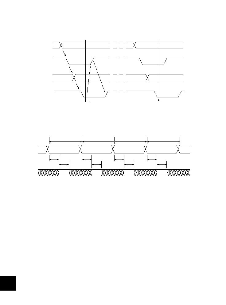
MOTOROLA
B-18
MC68HC05X16
Rev. 1
MC68HC705X32
15
Figure B-4 Timing diagram with handshake
Figure B-5 Parallel EPROM loader timing diagram
Data read
Data read
Address
HDSK out
(PC5)
Data
HDSK in
(PC6)
F29
t
COOE
t
ADE
t
DHE
Address
Data
t
ADE
t
DHE
t
ADE
t
DHE
t
ADE
t
DHE
t
COOE
t
COOE
t
CDDE
t
ADE
max (address to data delay)
5 machine cycles
t
DHA
min (data hold time)
14 machine cycles
t
COOE
(load cycle time)
117 machine cycles < t
COOE
< 150 machine cycles
t
CDDE
(programming cycle time)
t
COOE
+ t
PROG
(5ms nominal for EPROM; 10ms for EEPROM1))
1 machine cycle = 1/(2f
0
(Xtal))
200

MC68HC05X16
Rev. 1
MOTOROLA
B-19
MC68HC705X32
15
Warning: A minimum V
PP6R
voltage must be applied to the VPP6 pin at all times, including
power-on. Failure to do so could result in permanent damage to the device. Unless
otherwise stated, EPROM programming is guaranteed at ambient temperature (25
∞
C)
only.
Figure B-6 EPROM parallel bootstrap schematic diagram
VCC
28
1
VPP
PGM
27
PB0
PB1
PB2
PB3
PB4
PB5
PB6
PB7
PA0
PA1
PA2
PA3
PA4
PA5
PA6
PA7
VDD
OSC1
OSC2
TCAP1
IRQ
RESET
VSS
A0
A1
A2
A3
A4
A5
A6
A7
D0
D1
D2
D3
D4
D5
D6
D7
GND
OE
14
22
10
9
8
7
6
5
4
26
12
13
15
16
17
18
19
11
3
+5V
1
2
P1
GND
+5V
100mF
22pF
4.0 MHz
1N914
1k
1.0mF
22pF
100k
1N914
RESET
RUN
0.01mF
TDO
SCLK
RDI
VRL
TCAP2
PD7
PD6
PD5
PD3
PD2
PD1
PD0
PD4
+5V
3
V
PP
VPP6
PC7
PC5
PC4
PC3
PC2
PC1
PC0
PC6
24
21
23
2
A9
A8
A10
A12
CE
A11
A12
A11
A10
A9
A8
HDSK out
HDSK in
Short circuit if
handshake not used
100 k
NC
TCMP1
TCMP2
PLMA
PLMB
470
470
red LED
green LED
4k7
4k7
12 k
BC239C
BC309C
10k
27C256
+
+
VRH
red LED -- programming failed
green LED -- programming OK
25
1nF
1N5819
1 k
+
RAM
EPROM
green LED -- EPROM erased
47mF
+
Erase check & boot
EPROM erase
check
VPP1
red LED -- EPROM not erased
Boot
Erase check
A13
20
MC68HC705X32
MCU
A14
Verify
Program
EPROM
EPROM
201

MOTOROLA
B-20
MC68HC05X16
Rev. 1
MC68HC705X32
15
B.8.3
Serial RAM loader
This mode is similar to the RAM load/execute program for the MC68HC05X32 described in
Section 2.1.2.1
, with the additional features listed below.
Table B-5
shows the entry conditions
required for this mode.
If the first byte is less than $B0, the bootloader behaves exactly as the MC68HC05X32, i.e. count
byte followed by data stored in $0050 to $00FF. If the count byte is larger than RAM I (176 bytes)
then the code continues to fill RAM II then RAM III. In this case the count byte is ignored and the
program execution begins at $0051 once the total RAM area is filled or if no data is received for 5
milliseconds.
The user must take care when using branches or jumps as his code will be relocated in RAM I, II
and III. If the user intends to use the stack in his program, he should send NOP's to fill the desired
stack area.
In the RAM bootloader mode, all interrupt vectors are mapped to pseudo-vectors in RAM (see
Table B-6
). This allows programmers to use their own service-routine addresses. Each
pseudo-vector is allowed three bytes of space rather than the two bytes for normal vectors,
because an explicit jump (JMP) opcode is needed to cause the desired jump to the users
service-routine address.
B.8.3.1
Jump to start of RAM ($0051)
The Jump to start of RAM program will be executed then the device will be brought out of reset
with PD2 and PD3 at `1' and PD4 at `0'.
Table B-6 Bootstrap vector targets in RAM
Vector targets in RAM
SCI interrupt
$0063
Timer overflow
$0060
Timer output compare
$005D
Timer input capture
$005A
IRQ
$0057
SWI
$0054
202

MC68HC05X16
Rev. 1
MOTOROLA
B-21
MC68HC705X32
15
Figure B-7 RAM load and execute schematic diagram
VPP6
PC7
PB0
PB1
PB2
PB3
PB4
PB5
PB6
PB7
PA0
PA1
PA2
PA3
PA4
PA5
PA6
PA7
VDD
OSC1
OSC2
TCAP1
IRQ
RESET
VSS
P1
GND
+5V
1N914
1k
1.0mF
100k
1N914
RESET
RUN
0.01mF
V
PP
PC5
PC4
PC3
PC2
PC1
PC0
PC6
PLMA
PLMB
470
470
Red LED
Green LED
+
+
VRH
22mF
22mF
22mF
2 x 3K
1
2
3
4
8
6
7
5
11
12
13
14
15
16
5
3
2
1
22mF
RS232
Connector
MAX
232
+5V
9600 BD
8-bit
no parity
VRL
TCAP2
TCMP1
TCMP2
SCLK
NC
10nF
47mF
PD0
PD4
PD1
PD2
PD5
PD6
PD7
+
+
+
+
22pF
4.0 MHz
22pF
4k7
4k7
12 k
BC239C
BC309C
10k
1nF
1N5819
1 k
+
47mF
+
PD3
RDI
TDO
VPP1
MC68HC705X32
MCU
V
SS
203

MOTOROLA
B-22
MC68HC05X16
Rev. 1
MC68HC705X32
15
Figure B-8 Parallel RAM loader timing diagram
t
ADR
t
DHR
Address
Data
t
CR
PD4
t
EXR
max
t
HO
t
HI
max
PC5 out
PC6 in
204

MC68HC05X16
Rev. 1
MOTOROLA
B-23
MC68HC705X32
15
B.9
Electrical specifications
B.9.1
Maximum ratings
Note:
This device contains circuitry designed to protect against damage due to high
electrostatic voltages or electric fields. However, it is recommended that normal
precautions be taken to avoid the application of any voltages higher than those given in
the maximum ratings table to this high impedance circuit. For maximum reliability all
unused inputs should be tied to either V
SS
or V
DD
.
(1) All voltages are with respect to V
SS
.
(2) Maximum current drain per pin is for one pin at a time, limited by an external resistor.
Table B-7 Maximum ratings
Rating
Symbol
Value
Unit
Supply voltage
(1)
V
DD
≠ 0.5 to +7.0
V
Input voltage
V
IN
V
SS
≠ 0.5 to V
DD
+ 0.5
V
Input voltage
≠ Bootstrap mode (IRQ pin only)
V
IN
V
SS
≠ 0.5 to 2V
DD
+ 0.5
V
Operating temperature range
T
A
T
L
to T
H
≠40 to +125
∞
C
Storage temperature range
T
STG
≠ 65 to +150
∞
C
Current drain per pin
(2)
(Excluding VDD, VSS, VDD1 and VSS1)
≠ Source
≠ Sink
I
D
I
S
25
45
mA
mA
External oscillator frequency
f
OSC
22
MHz
205

MOTOROLA
B-24
MC68HC05X16
Rev. 1
MC68HC705X32
15
B.9.2
DC electrical characteristics
Table B-8 DC electrical characteristics
(V
DD
= 5.0 Vdc
±
10%, V
SS
= 0 Vdc, T
A
= ≠40
∞
C to +125
∞
C)
Characteristic
(1)
Symbol
Min
Typ
(2)
Max
Unit
Output voltage
I
LOAD
= ≠ 10
µ
A
I
LOAD
= +10
µ
A
V
OH
V
OL
V
DD
≠ 0.1
--
--
--
--
0.1
V
Output high voltage (I
LOAD
= 0.8mA)
PA0≠7, PB0≠7, PC0≠7, TCMP1, TCMP2,
Output high voltage (I
LOAD
= 1.6mA)
TDO, SCLK, PLMA, PLMB
Output high voltage (I
LOAD
= ≠300
µ
A)
OSC2
V
OH
V
OH
V
OH
V
DD
≠ 0.8
V
DD
≠ 0.8
V
DD
≠ 0.8
V
DD
≠ 0.2
V
DD
≠ 0.2
V
DD
≠ 0.3
--
--
V
Output low voltage (I
LOAD
= 1.6mA)
PA0≠7, PB0≠7, PC0≠7, TCMP1, TCMP2,
TDO, SCLK, PLMA, PLMB
Output low voltage (I
LOAD
= 1.6mA)
RESET
Output low voltage (I
LOAD
= ≠100
µ
A)
OSC2
V
OL
V
OL
V
OL
--
0.1
0.2
0.2
0.4
0.6
0.4
V
Input high voltage
PA0≠7, PB0≠7, PC0≠7, PD0≠7, OSC1, IRQ,
RESET, TCAP1, TCAP2, RDI, CANE, MDS, NWOI
V
IH
0.7V
DD
--
V
DD
V
Input low voltage
PA0≠7, PB0≠7, PC0≠7, PD0≠7, OSC1, IRQ,
RESET, TCAP1, TCAP2, RDI, CANE, MDS, NWOI
V
IL
V
SS
--
0.2V
DD
V
Can comparator I
DD
(I
DD1
)
(3)(4)(5)
Supply current in DIV2 mode
RUN: CAN active
(6)
STOP: CAN active
WAIT: CAN asleep
(7)
STOP: CAN asleep
I
DD1
I
DD1
I
DD1
I
DD1
--
--
--
--
360
360
32
10
900
900
100
30
µ
A
µ
A
µ
A
µ
A
MCU I
DD
(3)(4)(8)
Supply current in DIV 2 mode
RUN (SM = 0): CAN active
RUN (SM = 1): CAN active
WAIT (SM = 0): CAN active
WAIT (SM =1): CAN active
WAIT (SM = 0): CAN asleep
WAIT (SM = 1): CAN asleep
STOP: CAN active
STOP: CAN asleep
I
DD
I
DD
I
DD
I
DD
I
DD
I
DD
I
DD
I
DD
--
--
--
--
--
--
--
--
7
2.2
2.4
1.9
1.3
0.7
0.5
90
11.4
3.9
4.4
3.2
2.7
0.9
1.5
300
mA
mA
mA
mA
mA
mA
mA
µ
A
MCU I
DD
(3)(5)(8)
Supply current
RUN (SM = 0): CAN active
RUN (SM = 1): CAN active
WAIT (SM = 0): CAN active
WAIT (SM =1): CAN active
WAIT (SM = 0): CAN asleep
WAIT (SM = 1): CAN asleep
STOP: CAN active
STOP: CAN asleep
I
DD
I
DD
I
DD
I
DD
I
DD
I
DD
I
DD
I
DD
--
--
--
--
--
--
--
--
3.9
1.2
1.4
1.0
1.1
0.6
0.16
90
7
2.9
3.2
2.6
2
1.75
1.5
300
mA
mA
mA
mA
mA
mA
mA
µ
A
High-Z leakage current
PA0≠7, PB0≠7, PC0≠7, TDO, RESET, SCLK
I
IL
--
±
0.2
±
1
µ
A
206

MC68HC05X16
Rev. 1
MOTOROLA
B-25
MC68HC705X32
15
(1) All I
DD
measurements taken with suitable decoupling capacitors across the power supply to suppress the transient
switching currents inherent in CMOS designs (see Section 2).
(2) Typical values are at mid point of voltage range and at 25
∞
C only.
(3) RUN and WAIT I
DD
: measured using an external square-wave clock source, refer to
Figure 2-6
(c); all inputs 0.2 V
from rail; no DC loads; maximum load on outputs 50pF (20pF on OSC2).
STOP/WAIT I
DD
: all ports configured as inputs; V
IL
= 0.2 V and V
IH
= V
DD
≠ 0.2 V: STOP I
DD
measured with
OSC1 = V
DD
. WAIT I
DD
is affected linearly by the OSC2 capacitance.
(4) f
OSC
= 8 MHz; f
BUS
= 4 MHz; f
CAN
= 4 MHz
(5) f
OSC
= 4.4 MHz; f
BUS
= 2.2 MHz; f
CAN
= 2.2 MHz
(6) These limits are also applicable under the following conditions:
MCU RUN mode/SLOW mode/CAN active
MCU WAIT mode/SLOW mode/CAN active
MCU WAIT mode/CAN active
(7) These limits are also applicable under the following conditions:
MCU WAIT mode/SLOW mode/CAN asleep
(8) These currents are the summation of the MCU current + CAN current (I
DD
+ I
DD1
)
(9) Current injection is guaranteed but not tested.
Functionality of the MCU is guaranteed during injection of dc current up to the maximum specified level.
The maximum specified current for each port is the sum of the magnitudes of the currents on each side of the
individual port pins.
Some disturbance of the A/D accuracy is possible during an injection event and is dependent on board layout,
power supply decoupling and reference voltage decoupling configurations.
Input current
OSC1=V
DD
(OSC2=V
SS
)
Input current
OSC1=V
SS
(OSC2=V
DD
)
I
FH
I
FL
≠10
--
--
--
--
+10
µ
A
Input current
IRQ, TCAP1, TCAP2, RDI,
PD0/AN0-PD7/AN7 (channel not selected)
I
IN
--
±
0.2
±
1
µ
A
Capacitance
Ports (as input or output), RESET, TDO, SCLK
IRQ, TCAP1, TCAP2, OSC1, RDI
PD0/AN0≠PD7/AN7 (A/D off)
PD0/AN0≠PD7/AN7 (A/D on)
C
OUT
C
IN
C
IN
C
IN
--
--
--
--
--
--
12
22
12
8
--
--
pF
pF
pF
pF
DC injection current
(9)
Port A (PA0≠PA7)
Port B (PB0≠PB7)
|I
INJ
|
|I
INJ
|
--
--
--
--
10
10
mA
mA
Table B-8 DC electrical characteristics (Continued)
(V
DD
= 5.0 Vdc
±
10%, V
SS
= 0 Vdc, T
A
= ≠40
∞
C to +125
∞
C)
Characteristic
(1)
Symbol
Min
Typ
(2)
Max
Unit
207
MOTOROLA
B-26
MC68HC05X16
Rev. 1
MC68HC705X32
15
B.9.3
EPROM electrical characteristics
(1)
Typical values are at mid point of voltage range and at 25
∞
C only.
(A) F
MCU
> 2.2 MHz
(B) F
MCU
2.2 MHz
Note:
Use of programming times between 5ms and 20ms will not affect the product
reliability.
Table B-9 EPROM electrical characteristics
(V
DD
= 5.0 Vdc
±
10%, V
SS
= 0 Vdc, T
A
= ≠40
∞
C to +125
∞
C, f
MCU
4MHz)
Characteristic
Symbol
Min
Typ
(1)
Max
Unit
EPROM
Absolute maximum voltage
Programming voltage
Programming current
Read voltage
(A)
Read voltage
(B)
Read current
V
PP6
max
V
PP6
I
PP6
V
PP6R
V
PP6R
I
PP6R
V
DD
14.5
--
V
DD
≠ 0.35
V
DD
≠ 0.5
--
--
15
50
--
--
100
18
16
64
V
DD
V
DD
150
V
V
mA
V
V
µ
A
EPROM programming time
t
PROG
5
--
20
ms
208

MC68HC05X16
Rev. 1
MOTOROLA
B-27
MC68HC705X32
15
B.9.4
Control timing
(1) For bus frequencies less than 2 MHz, the internal RC oscillator should be used when
programming the EEPROM.
(2) Since a 2-bit prescaler in the timer must count four external cycles (t
cyc
), this is the limiting
factor in determining the timer resolution.
(3) The minimum period t
TLTL
should not be less than the number of cycle times it takes to
execute the capture interrupt service routine plus 24 t
cyc
.
(4) The minimum period t
ILIL
should not be less than the number of cycle times it takes to
execute the interrupt service routine plus 21 t
cyc
.
(5) At a temperature of 85
∞
C.
(6) Refer to Reliability Monitor Report (current quarterly issue) for current failure rate
information.
Table B-10 Control timing
(V
DD
= 5.0 Vdc
±
10%, V
SS
= 0 Vdc, T
A
= ≠40
∞
C to +125
∞
C)
Characteristic
Symbol
Min
Max
Unit
Frequency of operation
Oscillator frequency
MCAN module clock frequency
MCU bus frequency
f
OSC
f
CAN
f
MCU
0
0
0
22
11
4
MHz
MHz
MHz
Cycle time (see
Figure 10-1
)
t
CYC
455
--
ns
Crystal oscillator start-up time (see
Figure 10-1
)
t
OXOV
--
100
ms
Stop recovery start-up time (crystal oscillator)
t
ILCH
100
ms
A/D converter stabilization time
t
ADON
500
µ
s
External RESET input pulse width
t
RL
3.0
--
t
CYC
Power-on RESET output pulse width
4064 cycle
16 cycle
t
PORL
t
PORL
4064
16
--
--
t
CYC
t
CYC
Watchdog RESET output pulse width
t
DOGL
1.5
--
t
CYC
Watchdog time-out
t
DOG
6144
7168
t
CYC
EEPROM byte erase time
t
ERA
10
10
ms
EEPROM byte program time
(1)
t
PROG
10
10 ms
Timer (see
Figure B-9
)
Resolution
(2)
Input capture pulse width
Input capture pulse period
t
RESL
t
TH
, t
TL
t
TLTL
4
125
--
(3)
--
--
--
t
CYC
ns
t
CYC
Interrupt pulse width (edge-triggered)
t
ILIH
125
--
ns
Interrupt pulse period
t
ILIL
--
(4)
--
t
CYC
OSC1 pulse width
t
OH
, t
OL
90
--
ns
Write/erase endurance
(5)(6)
--
10000
cycles
Data retention
(5)(6)
--
10
years
Figure B-9 Timer relationship
External
signal
(TCAP1,
TCAP2)
t
TLTL
t
TH
t
TL
209

MOTOROLA
B-28
MC68HC05X16
Rev. 1
MC68HC705X32
15
B.9.5
A/D converter characteristics
(1) Performance verified down to 2.5V
VR, but accuracy is tested and guaranteed at
VR = 5V
±
10%.
(2) Source impedances greater than 10k
will adversely affect internal charging time during input sampling.
(3) The external system error caused by input leakage current is approximately equal to the product of R source and input
current. Input current to A/D channel will be dependent on external source impedance (see
Figure 9-2
).
Table B-11 A/D characteristics
(V
DD
= 5.0 Vdc
±
10%, V
SS
= 0 Vdc, T
A
= ≠40
∞
C to +125
∞
C)
Characteristic
Parameter
Min
Max
Unit
Resolution
Number of bits resolved by the A/D
8
--
Bit
Non-linearity
Max deviation from the best straight line through the A/D
transfer characteristics
(V
RH
= V
DD
and V
RL
= 0V)
--
±
0.5
LSB
Quantization error
Uncertainty due to converter resolution
--
±
0.5
LSB
Absolute accuracy
Difference between the actual input voltage and the
full-scale equivalent of the binary code output code for all
errors
--
±
1
LSB
Conversion range
Analog input voltage range
V
RL
V
RH
V
V
RH
Maximum analog reference voltage
V
RL
V
DD
+ 0.1
V
V
RL
Minimum analog reference voltage
V
SS
≠ 0.1
V
RH
V
V
R
(1)
Minimum difference between V
RH
and V
RL
3
--
V
Conversion time
Total time to perform a single analog to digital conversion
a. External clock (OSC1, OSC2)
b. Internal RC oscillator
--
--
32
32
t
CYC
µ
s
Monotonicity
Conversion result never decreases with an increase in
input voltage and has no missing codes
GUARANTEED
Zero input reading
Conversion result when V
IN
= V
RL
00
--
Hex
Full scale reading
Conversion result when V
IN
= V
RH
--
FF
Hex
Sample acquisition time
Analog input acquisition sampling
a. External clock (OSC1, OSC2)
b. Internal RC oscillator
(2)
--
--
12
12
t
CYC
µ
s
Sample/hold capacitance Input capacitance on PD0/AN0≠PD7/AN7
--
12
pF
Input leakage
(3)
Input leakage on A/D pins PD0/AN0≠PD7/AN7, VRL, VRH
--
1
µ
A
210

MC68HC05X16
Rev. 1
MOTOROLA
B-29
MC68HC705X32
15
B.9.6
MCAN bus interface DC electrical characteristics
B.9.7
MCAN bus interface control timing characteristics
(1) Maximum DC current should comply with maximum ratings.
Table B-12 MCAN bus interface DC electrical characteristics
(V
DD
= 5.0 Vdc
±
10%, V
SS
= 0 Vdc, T
A
= ≠40
∞
C to +125
∞
C)
Characteristic
Symbol
Min
Max
Unit
MCAN bus input comparator: pins RX0 and RX1
Input voltage
Common mode range
Latch-up trigger current
(1)
Input offset voltage
Hysteresis
V
IN
C
MR
I
LT
V
OFS
V
HYS
0.5
1.5
≠100
≠30
1
V
DD
+0.5
V
DD
≠1.5
+100
+30
22
V
V
mA
mV
mV
V
DD
˜
2 generator: pin VDDH
Output voltage difference to V
DD
˜
2 for
≠100
µ
A < I
OUT
< +100
µ
A
Output current
Latch-up trigger current
1
DV
OUT
I
OUT
I
LT
≠200
≠100
≠100
+200
+100
+100
mV
µ
A
mA
MCAN bus output driver: pins TX0 and TX1
Source current per pin (V
OUT
= V
DD
≠1.0V)
Sink current per pin (V
OUT
= 1.0V)
Latch-up trigger current
1
I
OH
I
OL
I
LT
≠10
10
≠100
--
--
+100
mA
mA
mA
(V
DD
= 5.0 Vdc
±
2%, V
SS
= 0 Vdc, T
A
= ≠40
∞
C to +125
∞
C)
Characteristic
Symbol
Min
Max
Unit
V
DD
˜
2 generator: pin VDDH
Output voltage difference to V
DD
˜
2 for
≠100
µ
A < I
OUT
< +100
µ
A
DV
OUT
≠180
+180
mV
Table B-13 MCAN bus interface control timing characteristics
(4.5V
V
DD
5.5V, V
SS
= 0 Vdc, T
A
= ≠40
∞
C to +125
∞
C)
Characteristic
Symbol
Min
Max
Unit
MCAN bus output driver
Rise and fall time (C
LOAD
= 100pF)
T
RF
--
25
ns
211

MOTOROLA
B-30
MC68HC05X16
Rev. 1
MC68HC705X32
15
THIS PAGE LEFT BLANK INTENTIONALLY
212

MC68HC05X16
Rev. 1
MOTOROLA
C-1
MC68HC05X32 HIGH SPEED OPERATION
15
C
MC68HC05X32
High speed operation
The following table of electrical characteristics applies only to the MC68HC05X32 operating with
a 4 MHz bus speed. For all other information relating to this device (except ordering information,
which can be found in
Section 14
), please refer to
Appendix A
.
C.1
DC electrical characteristics
Note:
The 4MHz bus frequency is achievable only in divide by 2 and divide by 4 modes. It is
not possible in divide by 10 mode.
(1) All I
DD
measurements taken with suitable decoupling capacitors across the power supply to suppress the transient
switching currents inherent in CMOS designs (see Section 2).
(2) Typical values are at mid point of voltage range and at 25
∞
C only.
(3) RUN and WAIT I
DD
: measured using an external square-wave clock source, refer to
Figure 2-6
(c); all inputs 0.2 V
from rail; no DC loads; maximum load on outputs 50pF (20pF on OSC2).
STOP/WAIT I
DD
: all ports configured as inputs; V
IL
= 0.2 V and V
IH
= V
DD
≠ 0.2 V: STOP I
DD
measured with
OSC1 = V
DD
. WAIT I
DD
is affected linearly by the OSC2 capacitance.
(4) f
OSC
= 8 MHz; f
BUS
= 4 MHz; f
CAN
= 4 MHz.
(5) These currents are the summation of the MCU current + CAN current (I
DD
+ I
DD1
).
Table C-1 DC electrical characteristics
(V
DD
= 5.0 Vdc
±
10%, V
SS
= 0 Vdc, T
A
= ≠40
∞
C to +125
∞
C)
Characteristic
(1)
Symbol
Min
Typ
(2)
Max
Unit
MCU I
DD
(3)(4)(5)
Supply current
RUN (SM = 0): CAN active
RUN (SM = 1): CAN active
WAIT (SM = 0): CAN active
WAIT (SM =1): CAN active
WAIT (SM = 0): CAN asleep
WAIT (SM = 1): CAN asleep
STOP: CAN active
STOP: CAN asleep
I
DD
I
DD
I
DD
I
DD
I
DD
I
DD
I
DD
I
DD
--
--
--
--
--
--
--
--
5.8
2.1
2.6
2
1.1
0.6
0.5
90
11
5.5
5.5
5
2.2
1.2
1.5
300
mA
mA
mA
mA
mA
mA
mA
µ
A
213

MOTOROLA
C-2
MC68HC05X16
Rev. 1
MC68HC05X32 HIGH SPEED OPERATION
15
C.2
Control Timing
Table C-2 Control timing
(V
DD
= 5.0 Vdc
±
10%, V
SS
= 0 Vdc, T
A
= ≠40
∞
C to +125
∞
C)
Characteristic
Symbol
Min
Max
Unit
Frequency of operation
Oscillator frequency
MCAN module clock frequency
MCU bus frequency
f
OSC
f
CAN
f
MCU
0
0
0
16
4
4
MHz
MHz
MHz
Cycle time (see
Figure 10-1
)
t
CYC
250
--
ns
214

MC68HC05X16
Rev. 1
MOTOROLA
i
GLOSSARY
GLOSSARY
This section contains abbreviations and specialist words used in this data
sheet and throughout the industry. Further information on many of the terms
may be gleaned from Motorola's
M68HC11 Reference Manual,
M68HC11RM/AD, or from a variety of standard electronics text books.
$xxxx
The digits following the `$' are in hexadecimal format.
%xxxx
The digits following the `%' are in binary format.
A/D, ADC
Analog-to-digital (converter).
Bootstrap mode
In this mode the device automatically loads its internal memory from an
external source on reset and then allows this program to be executed.
Byte
Eight bits.
CAN
Controller area network.
CCR
Condition codes register; an integral part of the CPU.
CERQUAD
A ceramic package type, principally used for EPROM and high temperature
devices.
Clear
`0' -- the logic zero state; the opposite of `set'.
CMOS
Complementary metal oxide semiconductor. A semiconductor technology
chosen for its low power consumption and good noise immunity.
COP
Computer operating properly.
aka `watchdog'. This circuit is used to detect
device runaway and provide a means for restoring correct operation.
CPU
Central processing unit.
D/A, DAC
Digital-to-analog (converter).
EEPROM
Electrically erasable programmable read only memory.
aka `EEROM'.
EPROM
Erasable programmable read only memory. This type of memory requires
exposure to ultra-violet wavelengths in order to erase previous data.
aka
`PROM'.
ESD
Electrostatic discharge.
215

MOTOROLA
ii
MC68HC05X16
Rev. 1
GLOSSARY
Expanded mode
In this mode the internal address and data bus lines are connected to
external pins. This enables the device to be used in much more complex
systems, where there is a need for external memory for example.
EVS
Evaluation system. One of the range of platforms provided by Motorola for
evaluation and emulation of their devices.
HCMOS
High-density complementary metal oxide semiconductor. A semiconductor
technology chosen for its low power consumption and good noise immunity.
I/O
Input/output; used to describe a bidirectional pin or function.
Input capture
(IC) This is a function provided by the timing system, whereby an external
event is `captured' by storing the value of a counter at the instant the event
is detected.
Interrupt
This refers to an asynchronous external event and the handling of it by the
MCU. The external event is detected by the MCU and causes a
predetermined action to occur.
IRQ
Interrupt request. The overline indicates that this is an active-low signal
format.
K byte
A kilo-byte (of memory); 1024 bytes.
LCD
Liquid crystal display.
LSB
Least significant byte.
M68HC05
Motorola's family of 8-bit MCUs.
MCU
Microcontroller unit.
MI BUS
Motorola interconnect bus. A single wire, medium speed serial
communications protocol.
MSB
Most significant byte.
Nibble
Half a byte; four bits.
NRZ
Non-return to zero.
Opcode
The opcode is a byte which identifies the particular instruction and operating
mode to the CPU.
Operand
The operand is a byte containing information the CPU needs to execute a
particular instruction.
Output compare
(OC) This is a function provided by the timing system, whereby an external
event is generated when an internal counter value matches a predefined
value.
PLCC
Plastic leaded chip carrier package.
PLL
Phase-locked loop circuit. This provides a method of frequency
multiplication, to enable the use of a low frequency crystal in a high
frequency circuit.
216

MC68HC05X16
Rev. 1
MOTOROLA
iii
GLOSSARY
Pull-down, pull-up These terms refer to resistors, sometimes internal to the device, which are
permanently connected to either ground or V
DD
.
PWM
Pulse width modulation. This term is used to describe a technique where the
width of the high and low periods of a waveform is varied, usually to enable
a representation of an analog value.
QFP
Quad flat pack package.
RAM
Random access memory. Fast read and write, but contents are lost when
the power is removed.
RFI
Radio frequency interference.
RTI
Real-time interrupt.
ROM
Read-only memory. This type of memory is programmed during device
manufacture and cannot subsequently be altered.
RS-232C
A standard serial communications protocol.
SAR
Successive approximation register.
SCI
Serial communications interface.
Set
`1' -- the logic one state; the opposite of `clear'.
Silicon glen
An area in the central belt of Scotland, so called because of the
concentration of semiconductor manufacturers and users found there.
Single chip mode
In this mode the device functions as a self contained unit, requiring only I/O
devices to complete a system.
SPI
Serial peripheral interface.
Test mode
This mode is intended for factory testing.
TTL
Transistor-transistor logic.
UART
Universal asynchronous receiver transmitter.
VCO
Voltage controlled oscillator.
Watchdog
see `COP'.
Wired-OR
A means of connecting outputs together such that the resulting composite
output state is the logical OR of the state of the individual outputs.
Word
Two bytes; 16 bits.
XIRQ
Non-maskable interrupt request. The overline indicates that this has an
active-low signal format.
217

MOTOROLA
iv
MC68HC05X16
Rev. 1
GLOSSARY
THIS PAGE LEFT BLANK INTENTIONALLY
218

MC68HC05X16
Rev. 1
MOTOROLA
v
INDEX
INDEX
In this index numeric entries are placed first; page references in
italics indicate that the reference
is to a figure.
64-pin QFP mechanical drawing
13-2
64-pin QFP pinout
13-1
A
A ≠ accumulator
11-1
A/D converter
ADSTAT
4-5
block diagram
9-2
clock selection
9-4
AC7-AC0 bits in CACC
5-13
ADDATA ≠ A/D result data register
9-3
addressing modes
11-11
≠
11-13
ADON bit in ADSTAT
4-5
,
9-5
ADRC bit in ADSTAT
9-4
ADSTAT ≠ A/D status/control register
4-5
,
9-4
ADON ≠ A/D converter on bit
4-5
,
9-5
ADRC ≠ A/D RC oscillator control bit
9-4
CH3-CH0 ≠ A/D channel selection bits
9-5
COCO ≠ continuous conversion bit
9-4
alternate counter register
6-3
AM0-AM7 bits in CACM
5-14
AT bit in CCOM
5-9
B
BAUD ≠ baud rate register
7-18
SCP1, SCP0 ≠ serial prescaler select bits
7-18
SCR2, SCR1, SCR0 ≠ SCI rate select bits
7-19
SCT2, SCT1, SCT0 ≠ SCI rate select bits
7-18
baud rate selection
7-20
biphase mode
5-18
bit set/clear addressing mode
11-13
bit test and branch addressing mode
11-13
bit time calculation
5-17
block diagrams
A/D converter
9-2
COP watchdog system
10-4
MC68HC05X16
1-4
MC68HC05X32
A-2
MC68HC705X32
B-3
MCAN module
5-1
PLM system
8-1
programmable timer
6-2
SCI
7-2
slow mode divider
2-10
BRP5-BRP0 bits in CBT0
5-15
BS bit in CSTAT
5-10
C
CACC ≠ MCAN acceptance code register
5-13
AC7-AC0 ≠ acceptance code bits
5-13
CACM ≠ MCAN acceptance mask register
5-14
AM0-AM7 ≠ acceptance mask bits
5-14
CAF bit in EEPROM control
B-8
CAN ≠ see MCAN
CANE
B-2
C-bit in CCR
11-3
CBT0 ≠ MCAN bus timing register 0
5-14
BRP5-BRP0 ≠ baud rate prescalar bits
5-15
SJW1, SJW0 ≠ synchronization jump width bits
5-14
CBT1 ≠ MCAN bus timing register 1
5-16
SAMP ≠ sampling bit
5-16
TSEG22-TSEG10 ≠ time segment bits
5-16
CCNTRL ≠ MCAN control register
5-6
EIE ≠ error interrupt enable bit
5-6
MODE ≠ undefined mode bit
5-6
OIE ≠ overrun interrupt enable bit
5-6
RIE ≠ receive interrupt enable bit
5-7
RR ≠ reset request bit
5-7
SPD ≠ speed mode bit
5-6
TIE ≠ transmit interrupt enable bit
5-6
CCOM ≠ MCAN command register
5-7
AT ≠ abort transmission bit
5-9
COMPSEL ≠ comparator selector bit
5-8
COS ≠ clear overrun status bit
5-9
RRB ≠ release receive buffer bit
5-9
RX0, RX1 ≠ receive pin bits
5-8
SLEEP ≠ go to sleep bit
5-8
TR ≠ transmission request bit
5-9
CCR ≠ condition code register
11-2
ceramic resonator
2-13
CH3-CH0 bits in ADSTAT
9-5
219

MOTOROLA
vi
MC68HC05X16
Rev. 1
INDEX
CINT ≠ MCAN interrupt register
5-12
EIF ≠ error interrupt flag
5-12
OIF ≠ overrun interrupt flag
5-12
RIF ≠ receive interrupt flag
5-13
TIF ≠ transmit interrupt flag
5-12
WIF ≠ wake-up interrupt flag
5-12
CIRQ
10-11
clocks ≠ see oscillator clock
COCNTRL ≠ MCAN output control register
5-18
OCM1, OCM0 ≠ output control mode bits
5-18
COCO bit in ADSTAT
9-4
COMPSEL bit in CCOM
5-8
COP
10-3
block diagram
10-4
COS bit in CCOM
5-9
counter
6-1
alternate counter register
6-3
counter register
6-3
CPHA bit in SCCR1
7-12
CPOL bit in SCCR1
7-12
CPU
A ≠ accumulator
11-1
addressing modes
11-11
≠
11-13
CCR ≠ condition code register
11-2
instruction set
11-3
≠
11-10
PC ≠ program counter
11-2
programming model
11-1
SP ≠ stack pointer
11-2
stacking order
11-2
X ≠ index register
11-2
crystal
2-13
CSTAT ≠ MCAN status register
5-10
BS ≠ bus status bit
5-10
DO ≠ data overrun bit
5-11
ES ≠ error status bit
5-10
RBS ≠ receive buffer status bit
5-11
RS ≠ receive status bit
5-10
TBA ≠ transmit buffer access bit
5-11
TCS ≠ transmission complete status bit
5-11
TS ≠ transmit status bit
5-10
D
DB7-DB0 bits in TDS
5-21
direct addressing mode
11-11
DIV2, DIV8 bits in MOR
B-12
DLC3-DLC0 bits in TRTDL
5-20
DO bit in CSTAT
5-11
E
E1ERA bit in EEPROM control
3-5
E1LAT bit in EEPROM control
3-5
E1PGM bit in EEPROM control
3-5
E6LAT bit in EEPROM control
B-9
E6PGM bit in EEPROM control
B-9
ECLK bit in EEPROM control
3-5
,
4-3
EE1P bit in OPTR
3-8
,
B-11
EEPROM
erase operation
3-6
programming operation
3-7
read operation
3-6
EEPROM control register
3-4
,
B-8
CAF ≠ MCAN asleep flag
B-8
E1ERA ≠ erase/programming bit
3-5
E1LAT ≠ programming latch enable bit
3-5
E1PGM ≠ charge pump enable/disable bit
3-5
E6LAT ≠ EPROM program latch enable bit
B-9
E6PGM ≠ EPROM program enable bit
B-9
ECLK ≠ external clock option bit
3-5
,
4-3
WOIE ≠ wired-OR interrupt enable bit
B-8
EIE bit in CCNTRL
5-6
EIF bit in CINT
5-12
EPROM
MOR
B-12
program operation
B-8
read operation
B-7
ES bit in CSTAT
5-10
extended addressing mode
11-12
external clock
2-13
F
FE bit in SCSR
7-17
flow charts
interrupts
10-8
self check mode (MC68HC05X16)
2-2
STOP and WAIT
2-9
FOLV2, FOLV1 bits in TCR
6-5
H
H-bit in CCR
11-2
I
I-bit in CCR
11-3
ICF1, ICF2 bits in TSR
6-6
ICIE bit in TCR
6-4
ICR1, ICR2 ≠ input capture registers
6-7
ID10-ID3 bits in TBI
5-20
ID2-ID0 bits in TRTDL
5-20
IDLE bit in SCSR
7-16
IEDG1 bit in TCR
6-5
ILIE bit in SCCR2
7-14
immediate addressing mode
11-11
indexed addressing modes
11-12
inherent addressing mode
11-11
input capture
6-7
instruction set
11-3
≠
11-10
tables of instructions
11-5
≠
11-10
INTE bit in Miscellaneous
3-11
,
10-10
interrupts
220

MC68HC05X16
Rev. 1
MOTOROLA
vii
INDEX
CIRQ
10-11
flow chart
10-8
IRQ
10-11
maskable
10-9
nonmaskable
10-9
priorities
10-9
programmable timer
10-12
SCI
10-12
SWI
10-9
WOI
10-11
INTP, INTN bits in Miscellaneous
3-11
,
10-10
IRQ
2-11
,
10-11
L
LBCL bit in SCCR1
7-13
low power modes
2-3
SLOW
2-8
WAIT
2-7
M
M bit in SCCR1
7-11
mask options
MC68HC05X16
1-3
MC68HC05X16
block diagram
1-4
mask options
1-3
memory map
3-2
register outline
3-9
MC68HC05X32
block diagram
A-2
memory map
A-3
register outline
A-5
MC68HC705X32
block diagram
B-3
memory map
B-5
register outline
B-4
MCAN
biphase mode
5-18
block diagram
5-1
CANE
B-2
electrical characteristics
12-6
,
A-11
,
B-29
memory map
3-3
,
5-5
normal mode 1
5-19
normal mode 2
5-19
oscillator block diagram
5-15
output control bits
5-19
RBF
5-4
register outline
3-10
single wire operation
5-24
SLEEP
5-24
TBF
5-4
MDS
2-12
mechanical drawings
64-pin QFP
13-2
memory
EEPROM (MC68HC05X16)
3-4
EPROM (MC68HC705X32)
B-7
MCAN memory map
3-3
,
5-5
memory map (MC68HC05X16)
3-2
memory map (MC68HC05X32)
A-3
memory map (MC68HC705X32)
B-5
RAM (MC68HC05X16)
3-1
ROM (MC68HC05X16)
3-1
self-check ROM (MC68HC05X16)
3-3
Miscellaneous register
2-10
,
3-11
,
8-3
INTE ≠ external interrupt enable bit
3-11
,
10-10
INTP, INTN ≠ external interrupt sensitivity bits
10-10
INTP, INTN ≠ interrupt sensitivity bits
3-11
POR ≠ power-on reset bit
3-11
,
10-2
SFA, SFB ≠ slow or fast mode selection bits
3-11
,
8-3
SM ≠ slow mode selection bit
3-12
,
8-3
SM slow mode selection bit
2-10
WDOG ≠ watchdog enable/disable bit
3-12
,
10-4
MODE bit in CCNTRL
5-6
modes of operation
jump to any address
2-3
low power modes
2-3
self-check mode
2-2
serial RAM loader
2-3
single-chip mode
2-1
MOR ≠ mask option register
B-12
DIV2, DIV8 ≠ clock divide ratio select bits
B-12
PBPD, PCPD ≠ port B and C pull-down bits
B-13
RTIM ≠ reset time bit
B-12
RWAT ≠ watchdog after reset bit
B-12
WOI ≠ wired-OR interrupt enable bit
B-12
WWAT ≠ watchdog during WAIT bit
B-13
N
N-bit in CCR
11-3
NF bit in SCSR
7-17
normal mode 1
5-19
normal mode 2
5-19
NWOI
2-16
O
OCIE bit in TCR
6-4
OCM1, OCM0 bits in COCNTRL
5-18
OCR1, OCR2 ≠ output compare registers
6-9
OIE bit in CCNTRL
5-6
OIF bit in CINT
5-12
OLV2, OLV1 bits in TCR
6-5
OPTR ≠ EEPROM options register
B-11
EE1P ≠ EEPROM protect bit
B-11
SEC ≠ secure bit
B-11
OPTR ≠ options register
3-7
EE1P ≠ EEPROM protect bit
3-8
SEC ≠ security bit
3-8
OR bit in SCSR
7-17
order numbers
14-1
221

MOTOROLA
viii
MC68HC05X16
Rev. 1
INDEX
OSC1, OSC2
2-13
oscillator clock
ceramic resonator
2-13
crystal
2-13
external clock
2-13
OSC1, OSC2
2-13
output compare
6-9
P
PA0≠7, PB0≠7, PC0≠7
2-16
PBPD, PCPD bits in MOR
B-13
PC ≠ program counter
11-2
PD0/AN0≠PD7/AN7
2-16
pinouts
64-pin QFP
13-1
pins
CANE
B-2
IRQ
2-11
MDS
2-12
NWOI
2-16
OSC1, OSC2
2-13
PA0≠7, PB0≠7, PC0≠7
2-16
PD0/AN0≠PD7/AN7
2-16
PLMA, PLMB
2-15
RDI
2-12
,
7-6
RESET
2-11
,
10-3
RX0, RX1
2-17
SCLK
2-13
TCAP1, TCAP2
2-12
TCMP1, TCMP2
2-12
TDO
2-12
TX0, TX1
2-17
VDD, VSS
2-11
VDD1, VSS1
2-17
VDDH
2-17
VPP1
2-16
VPP6
B-2
VRH
2-16
VRL
2-16
PLM
6-11
block diagram
8-1
clock selection
8-4
Miscellaneous register
8-3
PLMA, PLMB ≠ pulse length modulation registers
8-2
PLMA, PLMB pins
2-15
POR bit in Miscellaneous
3-11
,
10-2
ports
data direction registers
4-6
data registers
4-4
logic levels
4-7
port A
4-2
port B
4-2
port C
4-3
port D
4-4
power-on reset
10-2
programmable timer
block diagram
6-2
counter
6-1
ICR1, ICR2
6-7
OCR1, OCR2
6-9
PLM
6-11
software force compare
6-11
TCR
6-4
timing diagrams
6-12
TSR
6-6
pulse length modulation ≠ see PLM
R
R8 bit in SCCR1
7-11
RBF ≠ receive buffer
5-4
RBI ≠ receive buffer identifier register
5-21
RBS bit in CSTAT
5-11
RDI ≠ receive data in
2-12
,
7-6
RDRF bit in SCSR
7-16
RDS ≠ receive data segment registers
5-22
RE bit in SCCR2
7-15
receiver wake-up
7-5
register outline
MC68HC05X16
3-9
MC68HC05X32
A-5
MC68HC705X32
B-4
MCAN
3-10
relative addressing mode
11-13
RESET
2-11
,
10-3
resets
COP
10-3
power-on
10-2
RESET pin
2-11
,
10-3
timing diagram
10-1
RIE bit in CCNTRL
5-7
RIE bit in SCCR2
7-14
RIF bit in CINT
5-13
ROM verification units
14-2
RR bit in CCNTRL
5-7
RRB bit in CCOM
5-9
RRTDL ≠ transmission request/DLC register
5-22
RS bit in CSTAT
5-10
RTIM bit in MOR
B-12
RTR bit in TRTDL
5-20
RVU
14-2
RWAT bit in MOR
B-12
RWU bit in SCCR2
7-15
RX0, RX1 bits in CCOM
5-8
RX0, RX1 pins
2-17
S
SAMP bit in CBT1
5-16
SBK bit in SCCR2
7-15
SCCR1 ≠ serial communications control register 1
7-10
CPHA ≠ clock phase
7-12
CPOL ≠ clock polarity bit
7-12
LBCL ≠ last bit clock
7-13
M ≠ mode (select character format)
7-11
222

MC68HC05X16
Rev. 1
MOTOROLA
ix
INDEX
R8 ≠ receive data bit 8
7-11
T8 ≠ transmit data bit 8
7-11
WAKE ≠ wake-up mode select bit
7-11
SCCR2 ≠ serial communications control register 2
7-14
ILIE ≠ idle line interrupt enable
7-14
RE ≠ receiver enable
7-15
RIE ≠ receiver interrupt enable
7-14
RWU ≠ receiver wake-up
7-15
SBK ≠ send break
7-15
TCIE ≠ transmit complete interrupt enable
7-14
TE ≠ transmitter enable
7-14
TIE ≠ transmit interrupt enable
7-14
SCDR ≠ serial communications data register
7-10
SCI
baud rate selection
7-20
block diagram
7-2
data format
7-5
receiver wake-up
7-5
start bit detection
7-6
timing diagrams
7-12
SCLK
2-13
SCP1, SCP0 bits in BAUD
7-18
SCR2, SCR1, SCR0 bits in BAUD
7-19
SCSR ≠ serial communications status register
7-16
FE ≠ framing error flag
7-17
IDLE ≠ idle line detected flag
7-16
NF ≠ noise error flag
7-17
OR ≠ overrun error flag
7-17
RDRF ≠ receive data register full flag
7-16
TC ≠ transmit complete flag
7-16
TDRE ≠ transmit data register empty flag
7-16
SCT2, SCT1, SCT0 bits in BAUD
7-18
SEC bit in OPTR
3-8
,
B-11
self-check mode
2-2
SFA, SFB bits in Miscellaneous
3-11
,
8-3
single-chip mode
2-1
SJW1, SJW0 bits in CBT0
5-14
SLEEP
5-24
SLEEP bit in CCOM
5-8
SLOW
2-8
SM bit in Miscellaneous
2-10
,
3-12
,
8-3
software force compare
6-11
SP ≠ stack pointer
11-2
SPD bit in CCNTRL
5-6
T
T8 bit in SCCR1
7-11
TBA bit in CSTAT
5-11
TBF ≠ transmit buffer
5-4
TBI ≠ transmit buffer identifier register
5-20
ID10-ID3 ≠ identifier bits
5-20
TC bit in SCSR
7-16
TCAP1, TCAP2
2-12
TCIE bit in SCCR2
7-14
TCMP1, TCMP2
2-12
TCR ≠ timer control register
6-4
FOLV2, FOLV1 ≠ force output compare bits
6-5
ICIE ≠ input capture interrupt enable
6-4
IEDG1 ≠ input edge bit
6-5
OCIE ≠ output compare interrupt enable
6-4
OLV2, OLV1 ≠ output level bits
6-5
TOIE ≠ timer overflow interrupt enable
6-4
TCS bit in CSTAT
5-11
TDO
SCI transmit data out
7-8
TDO ≠ transmit data out
2-12
TDRE bit in SCSR
7-16
TDS ≠ transmit data segment registers
5-21
DB7-DB0 ≠ data bits
5-21
TE bit in SCCR2
7-14
TIE bit in CCNTRL
5-6
TIE bit in SCCR2
7-14
TIF bit in CINT
5-12
timing diagrams
ECLK
4-3
programmable timer
6-12
reset
10-1
SCI data clock
7-12
TOF bit in TSR
6-6
TOIE bit in TCR
6-4
TR bit in CCOM
5-9
TRTDL ≠ transmission request/DLC register
5-20
DLC3-DLC0 ≠ data length code bits
5-20
ID2-ID0 ≠ identifier bits
5-20
RTR ≠ remote transmission request
5-20
TS bit in CSTAT
5-10
TSEG22-TSEG10 bits in CBT1
5-16
TSR ≠ timer status register
6-6
ICF1, ICF2 ≠ input capture flags
6-6
OCF1, OCF2 ≠ output compare flags
6-6
TOF ≠ timer overflow status flag
6-6
TX0, TX1
2-17
V
VDD, VSS
2-11
VDD1, VSS1
2-17
VDDH
2-17
VPP1
2-16
VPP6
B-2
VRH
2-16
VRL
2-16
W
WAIT
2-7
WAKE bit in SCCR1
7-11
watchdog ≠ see COP
WDOG bit in Miscellaneous
3-12
,
10-4
WIF bit in CINT
5-12
wired-OR interrupt ≠ see WOI
WOI
10-11
WOI bit in MOR
B-12
WOIE bit in EEPROM control
B-8
WWAT bit in MOR
B-13
223

MOTOROLA
x
MC68HC05X16
Rev. 1
INDEX
X
X ≠ index register
11-2
Z
Z-bit in CCR
11-3
224

CUSTOMER FEEDBACK QUESTIONNAIRE (MC68HC05X16/D)
Motorola wishes to continue to improve the quality of its documentation. We would welcome your feedback on the publication you
have just received. Having used the document, please complete this card (or a photocopy of it, if you prefer).
1.
How would you rate the quality of the document? Check one box in each category.
Excellent
Poor
Excellent
Poor
Organization
t t t t
Tables
t t t t
Readability
t t t t
Table of contents
t t t t
Understandability
t t t t
Index
t t t t
Accuracy
t t t t
Page size/binding
t t t t
Illustrations
t t t t
Overall impression
t t t t
Comments:
2.
What is your intended use for this document? If more than one option applies, please rank them (1, 2, 3).
Selection of device for new application
t
Other
t
Please specify:
System design
t
Training purposes
t
3.
How well does this manual enable you to perform the task(s) outlined in question 2?
Completely
Not at all
Comments:
t t t t
4.
How easy is it to find the information you are looking for?
Easy
Difficult
Comments:
t t t t
5.
Is the level of technical detail in the following sections sufficient to allow you to understand how the device functions?
Too little detail
Too much detail
t t t t t
t t t t t
t t t t t
t t t t t
t t t t t
t t t t t
t t t t t
t t t t t
t t t t t
t t t t t
t t t t t
t t t t t
t t t t t
t t t t t
t t t t t
Comments:
6.
Have you found any errors? If so, please comment:
7.
From your point of view, is anything missing from the document? If so, please say what:
≠ Cut along this line to remo
v
e
≠
¢
SECTION 1
INTRODUCTION
SECTION 2
MODES OF OPERATION AND PIN DESCRIPTIONS
SECTION 3
MEMORY AND REGISTERS
SECTION 4
INPUT/OUTPUT PORTS
SECTION 5
MOTOROLA CAN MODULE (MCAN)
SECTION 6
PROGRAMMABLE TIMER
SECTION 7
SERIAL COMMUNICATIONS INTERFACE
SECTION 8
PULSE LENGTH D/A CONVERTERS
SECTION 9
ANALOG TO DIGITAL CONVERTER
SECTION 10
RESETS AND INTERRUPTS
SECTION 11
CPU CORE AND INSTRUCTION SET
SECTION 12
ELECTRICAL SPECIFICATIONS
SECTION 13
MECHANICAL DATA
SECTION 14
ORDERING INFORMATION
SECTION 15
APPENDICES
225

13. Currently there is some discussion in the semiconductor industry regarding a move towards providing data sheets in electronic
form. If you have any opinion on this subject, please comment.
14. We would be grateful if you would supply the following information (at your discretion), or attach your card.
Name:
Phone No:
Position:
FAX No:
Department:
Company:
Address:
Thank you for helping us improve our documentation,
Graham Forbes, Technical Publications Manager, Motorola Ltd., Scotland.
≠ Cut along this line to remo
v
e
≠
≠ Third fold back along this line ≠
8.
How could we improve this document?
9.
How would you rate Motorola's documentation?
Excellent
Poor
≠ In general
t t t t
≠ Against other semiconductor suppliers
t t t t
10. Which semiconductor manufacturer provides the best technical documentation?
11. Which company (in any field) provides the best technical documentation?
12. How many years have you worked with microprocessors?
Less than 1 year
t
1≠3
years
t
3≠5 years
t
More than 5 years
t
By air mail
Par avion
NE PAS AFFRANCHIR
IBRS NUMBER PHQ-B/207/G
CCRI NUMERO PHQ-B/207/G
REPONSE PAYEE
GRANDE-BRETAGNE
Motorola Ltd.,
Colvilles Road,
Kelvin Industrial Estate,
EAST KILBRIDE,
G75 8BR.
GREAT BRITAIN.
F.A.O. Technical Publications Manager
(re: MC68HC05X16/D)
NO STAMP REQUIRED
≠ First f
old bac
k along this line ≠
Semiconductor Products Sector
≠ Second fold back along this line ≠
≠ Finally, tuck this edge into opposite flap ≠
¢
226

1
2
3
4
5
6
7
8
9
10
11
12
13
14
15
227
INTRODUCTION
MODES OF OPERATION AND PIN DESCRIPTIONS
MEMORY AND REGISTERS
INPUT/OUTPUT PORTS
MOTOROLA CAN MODULE (MCAN)
PROGRAMMABLE TIMER
SERIAL COMMUNICATIONS INTERFACE
PULSE LENGTH D/A CONVERTERS
ANALOG TO DIGITAL CONVERTER
RESETS AND INTERRUPTS
CPU CORE AND INSTRUCTION SET
ELECTRICAL SPECIFICATIONS
MECHANICAL DATA
ORDERING INFORMATION
APPENDICES

1
2
3
4
5
6
7
8
9
10
11
12
13
14
15
INTRODUCTION
MODES OF OPERATION AND PIN DESCRIPTIONS
MEMORY AND REGISTERS
INPUT/OUTPUT PORTS
MOTOROLA CAN MODULE (MCAN)
PROGRAMMABLE TIMER
SERIAL COMMUNICATIONS INTERFACE
PULSE LENGTH D/A CONVERTERS
ANALOG TO DIGITAL CONVERTER
RESETS AND INTERRUPTS
CPU CORE AND INSTRUCTION SET
ELECTRICAL SPECIFICATIONS
MECHANICAL DATA
ORDERING INFORMATION
APPENDICES
228

2
1
3
4
5
6
7
8
9
10
11
12
13
14
15

2
1
3
4
5
6
7
8
9
10
11
12
13
14
15
How to reach us:
USA/EUROPE/Locations Not Listed: Motorola Literature Distribution; P.O. Box 5405; Denver,
Colorado 80217.1-800-441-2447 or 1-303-675-2140
MfaxTM: RMFAX0@email.sps.mot.com, http://sps.motorola.com/mfax/ ≠ TOUCHTONE 1-602-244-6609
Motorola Fax Back System
INTERNET: http://motorola.com/sps/
JAPAN: Nippon Motorola Ltd.; Tatsumi-SPD-JLDC, 6F Seibu-Butsuryu-Center, 3-14-2 Tatsumi Koto-Ku,
Tokyo 135, Japan. 81-3-3521-8315
ASIA/PACIFIC: Motorola Semiconductors H.K. Ltd.; 8B Tai Ping Industrial Park, 51 Ting Kok Road,
Tai Po, N.T., Hong Kong. 852-26629298
Customer Focus Center: 1-800-521-6274
Mfax is a trademark of Motorola, Inc.
