 | –≠–ª–µ–∫—Ç—Ä–æ–Ω–Ω—ã–π –∫–æ–º–ø–æ–Ω–µ–Ω—Ç: LM358D | –°–∫–∞—á–∞—Ç—å:  PDF PDF  ZIP ZIP |
LM358, LM258,
LM2904, LM2904V
SEMICONDUCTOR
TECHNICAL DATA
DUAL DIFFERENTIAL INPUT
OPERATIONAL AMPLIFIERS
ORDERING INFORMATION
PIN CONNECTIONS
Order this document by LM358/D
D SUFFIX
PLASTIC PACKAGE
CASE 751
(SO≠8)
N SUFFIX
PLASTIC PACKAGE
CASE 626
1
1
8
8
VEE/Gnd
Inputs A
Inputs B
Output B
Output A
VCC
≠
≠
+
+
1
2
3
4
8
7
6
5
(Top View)
Device
Operating
Temperature Range
Package
LM2904VD
LM2904VN
LM258D
LM258N
LM358D
LM358N
SO≠8
Plastic DIP
SO≠8
Plastic DIP
SO≠8
Plastic DIP
TA = ≠40
∞
to +125
∞
C
TA = ≠25
∞
to +85
∞
C
TA = 0
∞
to +70
∞
C
LM2904D
LM2904N
SO≠8
Plastic DIP
TA = ≠40
∞
to +105
∞
C
1
MOTOROLA ANALOG IC DEVICE DATA
Dual Low Power
Operational Amplifiers
Utilizing the circuit designs perfected for recently introduced Quad
Operational Amplifiers, these dual operational amplifiers feature 1) low
power drain, 2) a common mode input voltage range extending to
ground/VEE, 3) single supply or split supply operation and 4) pinouts
compatible with the popular MC1558 dual operational amplifier. The LM158
series is equivalent to one≠half of an LM124.
These amplifiers have several distinct advantages over standard
operational amplifier types in single supply applications. They can operate at
supply voltages as low as 3.0 V or as high as 32 V, with quiescent currents
about one≠fifth of those associated with the MC1741 (on a per amplifier
basis). The common mode input range includes the negative supply, thereby
eliminating the necessity for external biasing components in many
applications. The output voltage range also includes the negative power
supply voltage.
∑
Short Circuit Protected Outputs
∑
True Differential Input Stage
∑
Single Supply Operation: 3.0 V to 32 V
∑
Low Input Bias Currents
∑
Internally Compensated
∑
Common Mode Range Extends to Negative Supply
∑
Single and Split Supply Operation
∑
Similar Performance to the Popular MC1558
∑
ESD Clamps on the Inputs Increase Ruggedness of the Device without
Affecting Operation
MAXIMUM RATINGS
(TA = +25
∞
C, unless otherwise noted.)
Rating
Symbol
LM258
LM358
LM2904
LM2904V
Unit
Power Supply Voltages
Vdc
Single Supply
VCC
32
26
Split Supplies
VCC, VEE
±
16
±
13
Input Differential Voltage
Range (Note 1)
VIDR
±
32
±
26
Vdc
Input Common Mode Voltage
Range (Note 2)
VICR
≠0.3 to 32
≠0.3 to 26
Vdc
Output Short Circuit Duration
tSC
Continuous
Junction Temperature
TJ
150
∞
C
Storage Temperature Range
Tstg
≠55 to +125
∞
C
Operating Ambient Temperature
Range
TA
∞
C
LM258
≠25 to +85
≠
LM358
0 to +70
≠
LM2904
≠
≠40 to +105
LM2904V
≠
≠40 to +125
NOTES: 1. Split Power Supplies.
2. For Supply Voltages less than 32 V for the LM258/358 and 26 V for the LM2904, the
absolute maximum input voltage is equal to the supply voltage.
©
Motorola, Inc. 1996
Rev 2
LM358, LM258, LM2904, LM2904V
2
MOTOROLA ANALOG IC DEVICE DATA
ELECTRICAL CHARACTERISTICS
(VCC = 5.0 V, VEE = Gnd, TA = 25
∞
C, unless otherwise noted.)
Ch
t
i ti
S
b l
LM258
LM358
LM2904
LM2904V
U it
Characteristic
Symbol
Min
Typ
Max
Min
Typ
Max
Min
Typ
Max
Min
Typ
Max
Unit
Input Offset Voltage
VCC = 5.0 V to 30 V (26 V for
LM2904, V), VIC = 0 V to VCC ≠1.7 V,
VO
]
1.4 V, RS = 0
VIO
mV
TA = 25
∞
C
≠
2.0
5.0
≠
2.0
7.0
≠
2.0
7.0
≠
≠
≠
TA = Thigh (Note 1)
≠
≠
7.0
≠
≠
9.0
≠
≠
10
≠
≠
13
TA = Tlow (Note 1)
≠
≠
2.0
≠
≠
9.0
≠
≠
10
≠
≠
10
Average Temperature Coefficient of Input
Offset Voltage
VIO/
T
≠
7.0
≠
≠
7.0
≠
≠
7.0
≠
≠
7.0
≠
µ
V/
∞
C
T
A
= T
high
to T
low
(Note 1)
Input Offset Current
IIO
≠
3.0
30
≠
5.0
50
≠
5.0
50
≠
5.0
50
nA
TA = Thigh to Tlow (Note 1)
≠
≠
100
≠
≠
150
≠
45
200
≠
45
200
Input Bias Current
IIB
≠
≠45
≠150
≠
≠45
≠250
≠
≠45
≠250
≠
≠45
≠250
TA = Thigh to Tlow (Note 1)
≠
≠50
≠300
≠
≠50
≠500
≠
≠50
≠500
≠
≠50
≠500
Average Temperature Coefficient of Input
Offset Current
IIO/
T
≠
10
≠
≠
10
≠
≠
10
≠
≠
10
≠
pA/
∞
C
TA = Thigh to Tlow (Note 1)
Input Common Mode Voltage Range
(Note 2),VCC = 30 V (26 V for LM2904, V)
VICR
0
≠
28.3
0
≠
28.3
0
≠
24.3
0
≠
24.3
V
VCC = 30 V (26 V for LM2904, V),
TA = Thigh to Tlow
0
≠
28
0
≠
28
0
≠
24
0
≠
24
Differential Input Voltage Range
VIDR
≠
≠
VCC
≠
≠
VCC
≠
≠
VCC
≠
≠
VCC
V
Large Signal Open Loop Voltage Gain
AVOL
V/mV
RL = 2.0 k
, VCC = 15 V, For Large VO
Swing,
50
100
≠
25
100
≠
25
100
≠
25
100
≠
TA = Thigh to Tlow (Note 1)
25
≠
≠
15
≠
≠
15
≠
≠
15
≠
≠
Channel Separation
CS
≠
≠120
≠
≠
≠120
≠
≠
≠120
≠
≠
≠120
≠
dB
1.0 kHz
f
20 kHz, Input Referenced
Common Mode Rejection
CMR
70
85
≠
65
70
≠
50
70
≠
50
70
≠
dB
RS
10 k
Power Supply Rejection
PSR
65
100
≠
65
100
≠
50
100
≠
50
100
≠
dB
Output Voltage≠High Limit (TA = Thigh to
Tlow) (Note 1)
VOH
V
VCC = 5.0 V, RL = 2.0 k
, TA = 25
∞
C
3.3
3.5
≠
3.3
3.5
≠
3.3
3.5
≠
3.3
3.5
≠
VCC = 30 V (26 V for LM2904, V),
RL = 2.0 k
26
≠
≠
26
≠
≠
22
≠
≠
22
≠
≠
VCC = 30 V (26 V for LM2904, V),
RL = 10 k
27
28
≠
27
28
≠
23
24
≠
23
24
≠
Output Voltage≠Low Limit
VOL
≠
5.0
20
≠
5.0
20
≠
5.0
20
≠
5.0
20
mV
VCC = 5.0 V, RL = 10 k
, TA = Thigh to
Tlow (Note 1)
Output Source Current
IO +
20
40
≠
20
40
≠
20
40
≠
20
40
≠
mA
VID = +1.0 V, VCC = 15 V
Output Sink Current
IO ≠
VID = ≠1.0 V, VCC = 15 V
10
20
≠
10
20
≠
10
20
≠
10
20
≠
mA
VID = ≠1.0 V, VO = 200 mV
12
50
≠
12
50
≠
≠
≠
≠
≠
≠
≠
µ
A
Output Short Circuit to Ground (Note 3)
ISC
≠
40
60
≠
40
60
≠
40
60
≠
40
60
mA
Power Supply Current (TA = Thigh to Tlow)
(Note 1)
ICC
mA
VCC = 30 V (26 V for LM2904, V),
VO = 0 V, RL =
≠
1.5
3.0
≠
1.5
3.0
≠
1.5
3.0
≠
1.5
3.0
VCC = 5 V, VO = 0 V, RL =
≠
0.7
1.2
≠
0.7
1.2
≠
0.7
1.2
≠
0.7
1.2
NOTES: 1. Tlow = ≠40
∞
C for LM2904
Thigh = +105
∞
C for LM2904
= ≠40
∞
C for LM2904V
= +125
∞
C for LM2904V
= ≠25
∞
C for LM258
= +85
∞
C for LM258
= 0
∞
C for LM358
= +70
∞
C for LM358
2. The input common mode voltage or either input signal voltage should not be allowed to go negative by more than 0.3 V. The upper end of the common
mode voltage range is VCC ≠1.7 V.
3. Short circuits from the output to VCC can cause excessive heating and eventual destruction. Destructive dissipation can result from simultaneous shorts
on all amplifiers.
LM358, LM258, LM2904, LM2904V
3
MOTOROLA ANALOG IC DEVICE DATA
Single Supply
Split Supplies
VCC
VEE/Gnd
3.0 V to VCC(max)
1
2
VCC
1
2
VEE
1.5 V to VCC(max)
1.5 V to VEE(max)
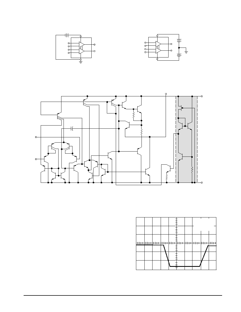
Representative Schematic Diagram
(One≠Half of Circuit Shown)
Output
Bias Circuitry
Common to Both
Amplifiers
VCC
VEE/Gnd
Inputs
Q2
Q3
Q4
Q5
Q26
Q7
Q8
Q6
Q9
Q11
Q10
Q1
2.4 k
Q25
Q22
40 k
Q13
Q14
Q15
Q16
Q19
5.0 pF
Q18
Q17
Q20
Q21
2.0 k
Q24
Q23
Q12
25
CIRCUIT DESCRIPTION
The LM258 series is made using two internally
compensated, two≠stage operational amplifiers. The first
stage of each consists of differential input devices Q20 and
Q18 with input buffer transistors Q21 and Q17 and the
differential to single ended converter Q3 and Q4. The first
stage performs not only the first stage gain function but also
performs the level shifting and transconductance reduction
functions. By reducing the transconductance, a smaller
compensation capacitor (only 5.0 pF) can be employed, thus
saving chip area. The transconductance reduction is
accomplished by splitting the collectors of Q20 and Q18.
Another feature of this input stage is that the input common
mode range can include the negative supply or ground, in
single supply operation, without saturating either the input
devices or the differential to single≠ended converter. The
second stage consists of a standard current source load
amplifier stage.
Each amplifier is biased from an internal≠voltage regulator
which has a low temperature coefficient thus giving each
amplifier good temperature characteristics as well as
excellent power supply rejection.
Large Signal Voltage
Follower Response
5.0
µ
s/DIV
1.0 V/DIV
VCC = 15 Vdc
RL = 2.0 k
TA = 25
∞
C
LM358, LM258, LM2904, LM2904V
4
MOTOROLA ANALOG IC DEVICE DATA
A
VOL
, OPEN LOOP
VOL
T
AGE GAIN (dB)
V
OR
, OUTPUT
VOL
T
AGE RANGE (V
)
pp
V
O
, OUTPUT
VOL
T
AGE
(mV)
V , INPUT
VOL
T
AGE
(V)
I
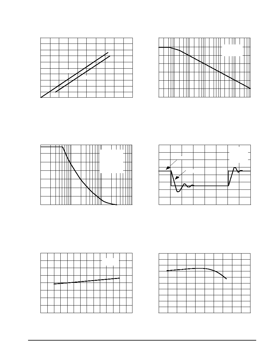
Figure 1. Input Voltage Range
Figure 2. Large≠Signal Open Loop Voltage Gain
Figure 3. Large≠Signal Frequency Response
Figure 4. Small Signal Voltage Follower
Pulse Response (Noninverting)
Figure 5. Power Supply Current versus
Power Supply Voltage
Figure 6. Input Bias Current versus
Supply Voltage
18
16
14
12
10
8.0
6.0
4.0
2.0
0
20
0
2.0
4.0
6.0
8.0
10
12
14
16
18
20
VCC/VEE, POWER SUPPLY VOLTAGES (V)
120
100
80
60
40
20
0
≠20
1.0
10
100
1.0 k
10 k
100 k
1.0 M
f, FREQUENCY (Hz)
14
12
10
8.0
6.0
4.0
2.0
0
1.0
10
100
1000
f, FREQUENCY (kHz)
550
500
450
400
350
300
250
200
0
0
1.0
2.0
3.0
4.0
5.0
6.0
7.0
8.0
t, TIME (ms)
2.4
2.1
1.8
1.5
1.2
0.9
0.6
0.3
0
0
5.0
10
15
20
25
30
35
VCC, POWER SUPPLY VOLTAGE (V)
VCC, POWER SUPPLY VOLTAGE (V)
90
80
70
0
2.0
4.0
6.0
8.0
10
12
14
16
18
20
I , POWER SUPPL
Y
CURRENT
(mA)
CC
I , INPUT
BIAS
CURRENT
(nA)
IB
Negative
Positive
VCC = 15 V
VEE = Gnd
TA = 25
∞
C
RL = 2.0 k
VCC = 15 V
VEE = Gnd
Gain = ≠100
RI = 1.0 k
RF = 100 k
Input
Output
TA = 25
∞
C
RL =
R
VCC = 30 V
VEE = Gnd
TA = 25
∞
C
CL = 50 pF
LM358, LM258, LM2904, LM2904V
5
MOTOROLA ANALOG IC DEVICE DATA
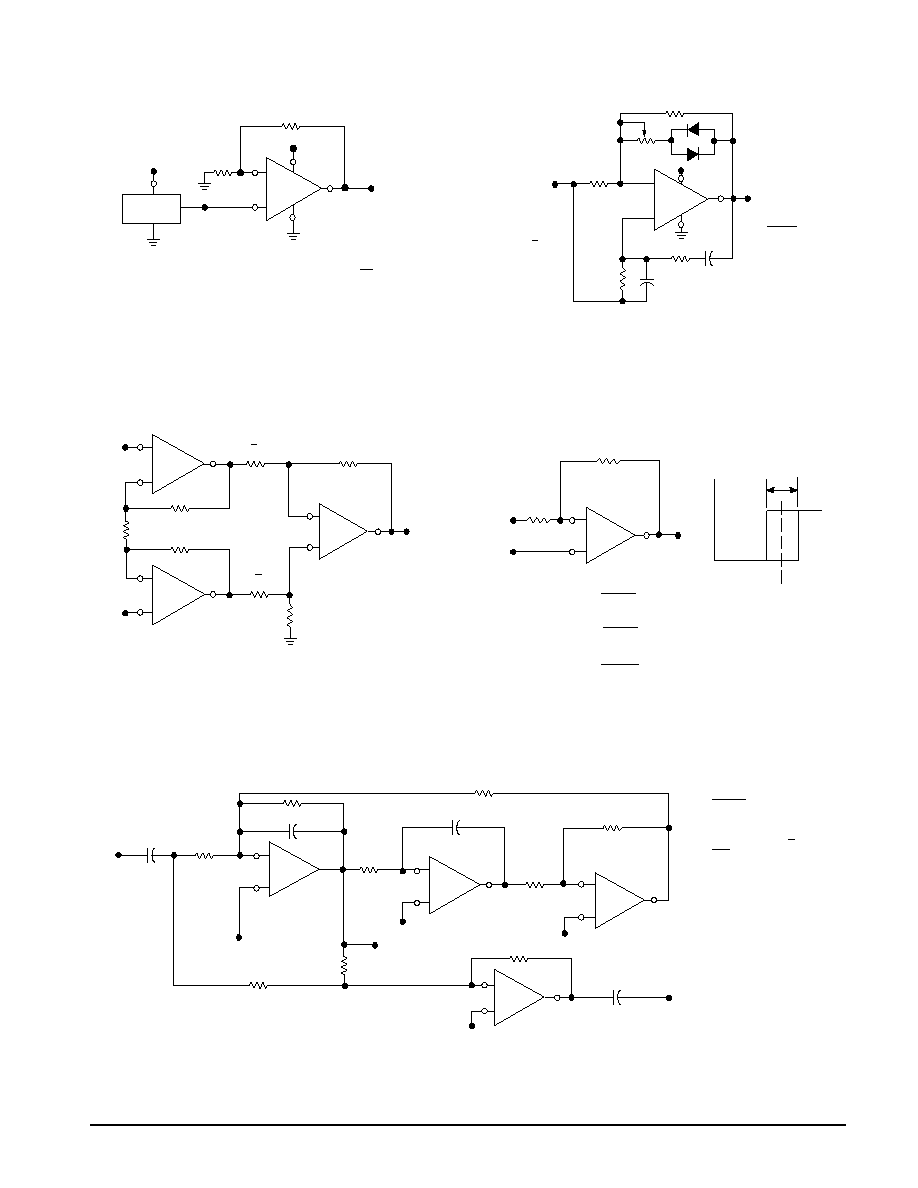
R1
2
1
R1
TBP
R1 + R2
R1
R1 + R2
1
Figure 7. Voltage Reference
Figure 8. Wien Bridge Oscillator
Figure 9. High Impedance Differential Amplifier
Figure 10. Comparator with Hysteresis
Figure 11. Bi≠Quad Filter
MC1403
1/2
LM358
≠
+
R1
VCC
VCC
VO
2.5 V
R2
50 k
10 k
Vref
Vref = VCC
2
5.0 k
R
C
R
C
+
1/2
LM358
≠
VO
2
RC
1
For: fo = 1.0 kHz
R = 16 k
C = 0.01
µ
F
eo
e1
e2
eo = C (1 + a + b) (e2 ≠ e1)
R1
a R1
b R1
R
C
R
≠
+
1/2
LM358
+
≠
≠
+
R
1/2
LM358
+
≠
R1
R2
VO
Vref
Vin
VOH
VO
VOL
VinL =
R1
(VOL ≠ Vref)+ Vref
VinH =
(VOH ≠ Vref) + Vref
H =
R1 + R2
(VOH ≠ VOL)
R1
≠
+
≠
+
≠
+
R
C
R2
R3
C1
100 k
R
C
R
C1
R2
100 k
Vin
Vref
Vref
Vref
Vref
Bandpass
Output
fo = 2
RC
R1 = QR
R2 =
R3 = TN R2
C1 = 10 C
1
Notch Output
Vref =
VCC
VO = 2.5 V (1 +
R1
R2
)
1
VCC
fo =
Hysteresis
1/2
LM358
1/2
LM358
1
C
R
VinL
VinH
Vref
1/2
LM358
1/2
LM358
1/2
LM358
1/2
LM358
TBP = Center Frequency Gain
TN = Passband Notch Gain
R
C
R1
R2
R3
For:
≠
+
fo
Q
TBP
TN
= 1.0 kHz
= 10
= 1
= 1
= 160 k
= 0.001
µ
F
= 1.6 M
= 1.6 M
= 1.6 M
Where: