 | –≠–ª–µ–∫—Ç—Ä–æ–Ω–Ω—ã–π –∫–æ–º–ø–æ–Ω–µ–Ω—Ç: LM393N | –°–∫–∞—á–∞—Ç—å:  PDF PDF  ZIP ZIP |
Device
Operating
Temperature Range
Package
LM393, LM393A,
LM293, LM2903,
LM2903V
SEMICONDUCTOR
TECHNICAL DATA
SINGLE SUPPLY, LOW POWER
DUAL COMPARATORS
ORDERING INFORMATION
LM293D
LM393D
TA = ≠25
∞
to +85
∞
C
TA = 0
∞
to +70
∞
C
SO≠8
Plastic DIP
PIN CONNECTIONS
Order this document by LM393/D
D SUFFIX
PLASTIC PACKAGE
CASE 751
(SO≠8)
N SUFFIX
PLASTIC PACKAGE
CASE 626
1
1
8
8
(Top View)
Gnd
Inputs A
Inputs B
Output B
Output A
VCC
≠
≠
+
+
1
2
3
4
8
7
6
5
LM393AN,N
LM2903D
LM2903N
TA = ≠40
∞
to +105
∞
C
SO≠8
Plastic DIP
SO≠8
LM2903VD
LM2903VN
TA = ≠40
∞
to +105
∞
C
SO≠8
Plastic DIP
1
MOTOROLA ANALOG IC DEVICE DATA
Low Offset Voltage
Dual Comparators
The LM393 series are dual independent precision voltage comparators
capable of single or split supply operation. These devices are designed to
permit a common mode range≠to≠ground level with single supply operation.
Input offset voltage specifications as low as 2.0 mV make this device an
excellent selection for many applications in consumer automotive, and
industrial electronics.
∑
Wide Single≠Supply Range: 2.0 Vdc to 36 Vdc
∑
Split≠Supply Range:
±
1.0 Vdc to
±
18 Vdc
∑
Very Low Current Drain Independent of Supply Voltage: 0.4 mA
∑
Low Input Bias Current: 25 nA
∑
Low Input Offset Current: 5.0 nA
∑
Low Input Offset Voltage: 2.0 mV (max) LM393A
5.0 mV (max) LM293/393
∑
Input Common Mode Range to Ground Level
∑
Differential Input Voltage Range Equal to Power Supply Voltage
∑
Output Voltage Compatible with DTL, ECL, TTL, MOS, and CMOS Logic
Levels
∑
ESD Clamps on the Inputs Increase the Ruggedness of the Device
without Affecting Performance
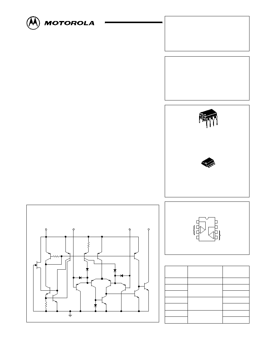
Representative Schematic Diagram
(Diagram shown is for 1 comparator)
VCC
+ Input
≠ Input
Output
Q3
R4
Q4
Q5
R2
Q6
Q14
Q16
Q15
Q12
Q11
Q10
Q9
Q8
Q2
Q1
F1
2.0 k
2.1 k
R1
4.6 k
©
Motorola, Inc. 1996
Rev 1

LM393, LM393A, LM293, LM2903, LM2903V
2
MOTOROLA ANALOG IC DEVICE DATA
MAXIMUM RATINGS
Rating
Symbol
Value
Unit
Power Supply Voltage
VCC
+36 or
±
18
Vdc
Input Differential Voltage Range
VIDR
36
Vdc
Input Common Mode Voltage Range
VICR
≠0.3 to +36
Vdc
Output Short Circuit≠to≠Ground
ISC
Continuous
mA
Output Sink Current (Note 1)
ISink
20
Power Dissipation @ TA = 25
∞
C
PD
570
mW
Derate above 25
∞
C
1/R
JA
5.7
mW/
∞
C
Operating Ambient Temperature Range
TA
∞
C
LM293
≠25 to +85
LM393, 393A
0 to +70
LM2903
≠40 to +105
LM2903V
≠40 to +125
Maximum Operating Junction Temperature
TJ(max)
∞
C
LM393, 393A, 2903, LM2903V
125
LM293
150
Storage Temperature Range
Tstg
≠65 to +150
∞
C
ELECTRICAL CHARACTERISTICS
(VCC = 5.0 Vdc, Tlow
TA
Thigh,* unless otherwise noted.)
Ch
i i
S
b l
LM393A
U i
Characteristic
Symbol
Min
Typ
Max
Unit
Input Offset Voltage (Note 2)
VIO
mV
TA = 25
∞
C
≠
±
1.0
±
2.0
Tlow
TA
Thigh
≠
≠
4.0
Input Offset Current
IIO
nA
TA = 25
∞
C
≠
±
50
±
50
Tlow
TA
Thigh
≠
≠
±
150
Input Bias Current (Note 3)
IIB
nA
TA = 25
∞
C
≠
25
250
Tlow
TA
Thigh
≠
≠
400
Input Common Mode Voltage Range (Note 4)
VICR
V
TA = 25
∞
C
0
≠
VCC ≠1.5
Tlow
TA
Thigh
0
≠
VCC ≠2.0
Voltage Gain RL
15 k
, VCC = 15 Vdc, TA = 25
∞
C
AVOL
50
200
≠
V/mV
Large Signal Response Time
≠
≠
300
≠
ns
Vin = TTL Logic Swing, Vref = 1.4 Vdc
VRL = 5.0 Vdc, RL = 5.1 k
, TA = 25
∞
C
Response Time (Note 5) VRL = 5.0 Vdc, RL = 5.1 k
, TA = 25
∞
C
tTLH
≠
1.3
≠
µ
s
Input Differential Voltage (Note 6)
All Vin
Gnd or V≠ Supply (if used)
VID
≠
≠
VCC
V
Output Sink Current
Vin
1.0 Vdc, Vin+ = 0 Vdc, VO
1.5 Vdc, TA = 25
∞
C
ISink
6.0
16
≠
mA
Output Saturation Voltage
VOL
mV
Vin
1.0 Vdc, Vin+ = 0 Vdc, ISink
4.0 mA, TA = 25
∞
C
≠
150
400
Tlow
TA
Thigh
≠
≠
700
* Tlow = 0
∞
C, Thigh = +70
∞
C for LM393/393A
NOTES: 1. The maximum output current may be as high as 20 mA, independent of the magnitude of VCC, output short circuits to VCC can cause excessive
heating and eventual destruction.
2. At output switch point, VO
]
1.4 Vdc, RS = 0
with VCC from 5.0 Vdc to 30 Vdc, and over the full input common mode range (0 V to VCC = ≠1.5 V).
3. Due to the PNP transistor inputs, bias current will flow out of the inputs. This current is essentially constant, independent of the output state, there
fore, no loading changes will exist on the input lines.
4. Input common mode of either input should not be permitted to go more than 0.3 V negative of ground or minus supply. The upper limit of common
mode range is VCC ≠1.5 V.
5. Response time is specified with a 100 mV step and 5.0 mV of overdrive. With larger magnitudes of overdrive faster response times are obtainable.
6. The comparator will exhibit proper output state if one of the inputs becomes greater than VCC, the other input must remain within the common mode
range. The low input state must not be less than ≠0.3 V of ground or minus supply.

LM393, LM393A, LM293, LM2903, LM2903V
3
MOTOROLA ANALOG IC DEVICE DATA
ELECTRICAL CHARACTERISTICS
(VCC = 5.0 Vdc, Tlow
TA
Thigh,* unless otherwise noted.)
Ch
i i
S
b l
LM393A
U i
Characteristic
Symbol
Min
Typ
Max
Unit
Output Leakage Current
IOL
µ
A
Vin≠ = 0 V, Vin+
1.0 Vdc, VO = 5.0 Vdc, TA= 25
∞
C
≠
0.1
≠
Vin≠ = 0 V, Vin+
1.0 Vdc, VO = 30 Vdc, Tlow
TA
Thigh
≠
≠
1.0
Supply Current
ICC
mA
RL =
Both Comparators, TA = 25
∞
C
≠
0.4
1.0
RL =
Both Comparators, VCC = 30 V
≠
1.0
2.5
ELECTRICAL CHARACTERISTICS
(VCC = 5.0 Vdc, Tlow
TA
Thigh, unless otherwise noted.)
Ch
i i
S
b l
LM392, LM393
LM2903, LM2903V
U i
Characteristic
Symbol
Min
Typ
Max
Min
Typ
Max
Unit
Input Offset Voltage (Note 2)
VIO
mV
TA = 25
∞
C
≠
±
1.0
±
5.0
≠
±
2.0
±
7.0
Tlow
TA
Thigh
≠
≠
9.0
≠
9.0
15
Input Offset Current
IIO
nA
TA = 25
∞
C
≠
±
5.0
±
50
≠
±
5.0
±
50
Tlow
TA
Thigh
≠
≠
±
150
≠
±
50
±
200
Input Bias Current (Note 3)
IIB
nA
TA = 25
∞
C
≠
25
250
≠
25
250
Tlow
TA
Thigh
≠
≠
400
≠
200
500
Input Common Mode Voltage Range (Note 3)
VICR
V
TA = 25
∞
C
0
≠
VCC ≠1.5
0
≠
VCC ≠1.5
Tlow
TA
Thigh
0
≠
VCC ≠2.0
0
≠
VCC ≠2.0
Voltage Gain
AVOL
50
200
≠
25
200
≠
V/mV
RL
15 k
, VCC = 15 Vdc, TA = 25
∞
C
Large Signal Response Time
≠
≠
300
≠
≠
300
≠
ns
Vin = TTL Logic Swing, Vref = 1.4 Vdc
VRL = 5.0 Vdc, RL = 5.1 k
, TA = 25
∞
C
Response Time (Note 5)
tTLH
≠
1.3
≠
≠
1.5
≠
µ
s
VRL = 5.0 Vdc, RL = 5.1 k
, TA = 25
∞
C
Input Differential Voltage (Note 6)
VID
≠
≠
VCC
≠
≠
VCC
V
All Vin
Gnd or V≠ Supply (if used)
Output Sink Current
ISink
6.0
16
≠
6.0
16
≠
mA
Vin
1.0 Vdc, Vin+ = 0 Vdc, VO
1.5 Vdc TA = 25
∞
C
Output Saturation Voltage
VOL
mV
Vin
1.0 Vdc, Vin+ = 0, ISink
4.0 mA, TA = 25
∞
C
≠
150
400
≠
≠
400
Tlow
TA
Thigh
≠
≠
700
≠
200
700
Output Leakage Current
IOL
nA
Vin≠ = 0 V, Vin+
1.0 Vdc, VO = 5.0 Vdc, TA = 25
∞
C
≠
0.1
≠
≠
0.1
≠
Vin≠ = 0 V, Vin+
1.0 Vdc, VO = 30 Vdc,
Tlow
TA
Thigh
≠
≠
1000
≠
≠
1000
Supply Current
ICC
mA
RL =
Both Comparators, TA = 25
∞
C
≠
0.4
1.0
≠
0.4
1.0
RL =
Both Comparators, VCC = 30 V
≠
≠
2.5
≠
≠
2.5
* Tlow = 0
∞
C, Thigh = +70
∞
C for LM393/393A
LM293 Tlow = ≠25
∞
C, Thigh = +85
∞
C
LM2903 Tlow = ≠40
∞
C, Thigh = +105
∞
C
LM2903V Tlow = ≠40
∞
C, Thigh = +125
∞
C
NOTES: 2. At output switch point, VO
]
1.4 Vdc, RS = 0
with VCC from 5.0 Vdc to 30 Vdc, and over the full input common mode range (0 V to VCC = ≠1.5 V).
3. Due to the PNP transistor inputs, bias current will flow out of the inputs. This current is essentially constant, independent of the output state, there
fore, no loading changes will exist on the input lines.
5. Response time is specified with a 100 mV step and 5.0 mV of overdrive. With larger magnitudes of overdrive faster response times are obtainable.
6. The comparator will exhibit proper output state if one of the inputs becomes greater than VCC, the other input must remain within the common mode
range. The low input state must not be less than ≠0.3 V of ground or minus supply.
LM393, LM393A, LM293, LM2903, LM2903V
4
MOTOROLA ANALOG IC DEVICE DATA
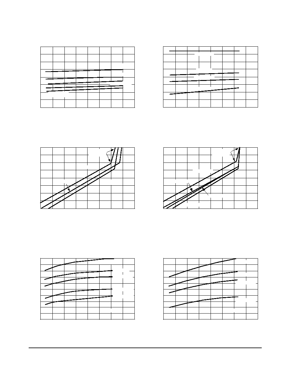
LM293/393,A
LM2903
Figure 1. Input Bias Current versus
Power Supply Voltage
Figure 2. Input Bias Current versus
Power Supply Voltage
Figure 3. Output Saturation Voltage
versus Output Sink Current
Figure 4. Output Saturation Voltage
versus Output Sink Current
Figure 5. Power Supply Current versus
Power Supply Voltage
Figure 6. Power Supply Current versus
Power Supply Voltage
VCC, SUPPLY VOLTAGE (Vdc)
VCC, SUPPLY VOLTAGE (Vdc)
VCC, SUPPLY VOLTAGE (Vdc)
VCC, SUPPLY VOLTAGE (Vdc)
ISink, OUTPUT SINK CURRENT (mA)
ISink, OUTPUT SINK CURRENT (mA)
I , INPUT
BIAS
CURRENT
(nA)
IB
V , SA
TURA
TION
VOL
T
AGE
(Vdc)
OL
I , SUPPL
Y
CURRENT
(mA)
CC
80
70
60
50
40
30
20
10
0
0
5.0
10
15
20
25
30
35
40
80
70
60
50
40
30
20
10
0
0
5.0
10
15
20
25
30
35
40
10
1.0
0.1
0.01
0.001
0.01
0.1
1.0
10
100
1.0
0.8
0.6
0.4
0.2
0
5.0
10
15
20
25
30
35
40
1.2
0.4
10
1.0
0.1
0.01
0.001
0.01
0.1
1.0
10
100
0
5.0
10
15
20
25
30
35
40
TA = 0
∞
C
TA = +25
∞
C
TA = +25
∞
C
TA = +85
∞
C
TA = ≠40
∞
C
TA = +70
∞
C
TA = +125
∞
C
RL =
R
TA = 0
∞
C
TA = +25
∞
C
TA = +25
∞
C
TA = 0
∞
C
TA = +25
∞
C
TA = ≠40
∞
C
TA = ≠40
∞
C
TA = 0
∞
C
TA = +25
∞
C
TA = +85
∞
C
1.0
0.8
0.6
I , SUPPL
Y
CURRENT
(mA)
CC
V , SA
TURA
TION
VOL
T
AGE
(Vdc)
OL
I , INPUT
BIAS
CURRENT
(nA)
IB
TA = +125
∞
C
RL =
R
TA = ≠55
∞
C
TA = +70
∞
C
TA = +125
∞
C
TA = ≠55
∞
C
Out of
Saturation
TA = +85
∞
C
Out of
Saturation
TA = ≠55
∞
C
TA = 0
∞
C

LM393, LM393A, LM293, LM2903, LM2903V
5
MOTOROLA ANALOG IC DEVICE DATA
APPLICATIONS INFORMATION
These dual comparators feature high gain, wide
bandwidth characteristics. This gives the device oscillation
tendencies if the outputs are capacitively coupled to the
inputs via stray capacitance. This oscillation manifests itself
during output transitions (VOL to VOH). To alleviate this
situation, input resistors < 10 k
should be used.
The addition of positive feedback (< 10 mV) is also
recommended. It is good design practice to ground all
unused pins.
Differential input voltages may be larger than supply
voltage without damaging the comparator's inputs. Voltages
more negative than ≠0.3 V should not be used.
Figure 7. Zero Crossing Detector
(Single Supply)
Figure 8. Zero Crossing Detector
(Split Supply)
Figure 9. Free≠Running Square≠Wave Oscillator
Figure 10. Time Delay Generator
Figure 11. Comparator with Hysteresis
10
D1 prevents input from going negative by more than 0.6 V.
R1 + R2 = R3
R3
R5
for small error in zero crossing.
Vin
10 k
D1
R1
8.2 k
6.8 k
R2
15 k
R3
+15 V
10 M
R5
220 k
R4
220 k
LM393
Vin(min)
[
0.4 V peak for 1% phase distortion (
).
*
+VCC
10 k
Vin
≠VEE
Vin
Vin(min)
VCC
VO
≠ VEE
LM393
≠
+
LM393
51 k
51 k
51 k
RL
10 k
VCC
VCC
VCC
VO
VO
t
0
1.0 M
0.001
µ
F
≠
+
LM393
VCC
VCC
VO
Vin
VO
+ Vref
Vref
Vref
0
0
0
VC
tO
t
``ON'' for t
tO +
t
where:
t = RC n (
Vref
VCC
)
R
RL
VC
C
LM393
≠
+
RS
VCC
RL
Vref
R1
R2
RS = R1 | | R2
Vth1 = Vref +
(VCC ≠Vref) R1
R1 + R2 + RL
Vth2 = Vref ≠
(Vref ≠VO Low) R1
R1 + R2
R1
t
≠
+
LM393
)
*
)