 | –≠–ª–µ–∫—Ç—Ä–æ–Ω–Ω—ã–π –∫–æ–º–ø–æ–Ω–µ–Ω—Ç: MAC212A6 | –°–∫–∞—á–∞—Ç—å:  PDF PDF  ZIP ZIP |
3≠83
Motorola Thyristor Device Data
Triacs
Silicon Bidirectional Thyristors
. . . designed primarily for full-wave ac control applications, such as light dimmers,
motor controls, heating controls and power supplies; or wherever full-wave silicon
gate controlled solid-state devices are needed. Triac type thyristors switch from a
blocking to a conducting state for either polarity of applied anode voltage with positive
or negative gate triggering.
∑
Blocking Voltage to 800 Volts
∑
All Diffused and Glass Passivated Junctions for Greater Parameter Uniformity
and Stability
∑
Small, Rugged, Thermowatt Construction for Low Thermal Resistance, High Heat
Dissipation and Durability
∑
Gate Triggering Guaranteed in Three Modes (MAC212 Series) or Four Modes
(MAC212A Series)
MAXIMUM RATINGS
(TJ = 25
∞
C unless otherwise noted.)
Rating
Symbol
Value
Unit
Repetitive Peak Off-State Voltage(1) (TJ = ≠40 to +125
∞
C,
1/2 Sine Wave 50 to 60 Hz, Gate Open)
MAC212-4, MAC212A4
MAC212-6, MAC212A6
MAC212-8, MAC212A8
MAC212-10, MAC212A10
VDRM
200
400
600
800
Volts
On-State Current RMS (TC = +85
∞
C)
Full Cycle Sine Wave 50 to 60 Hz
IT(RMS)
12
Amp
Peak Non-repetitive Surge Current (One Full Cycle, 60 Hz, TC = +85
∞
C)
preceded and followed by Rated Current
ITSM
100
Amp
Circuit Fusing Considerations (t = 8.3 ms)
I2t
40
A2s
Peak Gate Power (TC = +85
∞
C, Pulse Width = 10
µ
s)
PGM
20
Watts
Average Gate Power (TC = +85
∞
C, t = 8.3 ms)
PG(AV)
0.35
Watt
Peak Gate Current (TC = +85
∞
C, Pulse Width = 10
µ
s)
IGM
2
Amp
Operating Junction Temperature Range
TJ
≠40 to +125
∞
C
Storage Temperature Range
Tstg
≠40 to +150
∞
C
1. VDRM for all types can be applied on a continuous basis. Blocking voltages shall not be tested with a constant current source such that the
voltage ratings of the devices are exceeded.
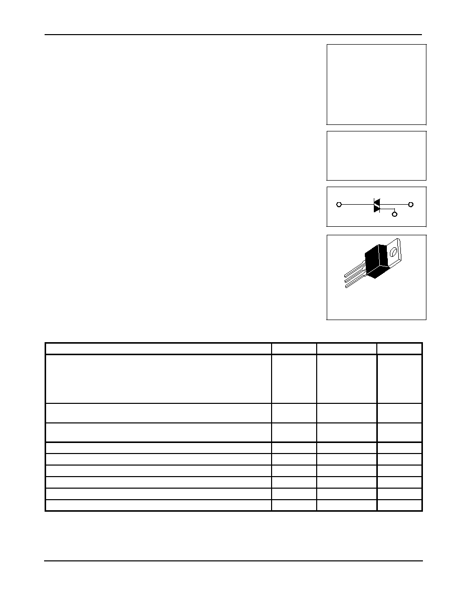
MOTOROLA
SEMICONDUCTOR TECHNICAL DATA
MAC212
Series
MAC212A
Series
CASE 221A-04
(TO-220AB)
STYLE 4
TRIACs
12 AMPERES RMS
200 thru 800 VOLTS
MT1
G
MT2

MAC212 Series MAC212A Series
3≠84
Motorola Thyristor Device Data
THERMAL CHARACTERISTICS
Characteristic
Symbol
Max
Unit
Thermal Resistance, Junction to Case
R
JC
2.1
∞
C/W
ELECTRICAL CHARACTERISTICS
(TC = 25
∞
C unless otherwise noted.)
Characteristic
Symbol
Min
Typ
Max
Unit
Peak Blocking Current (Either Direction)
(VD = Rated VDRM, Gate Open)
TJ = 25
∞
C
TJ = +125
∞
C
IDRM
--
--
--
--
10
2
µ
A
mA
Peak On-State Voltage (Either Direction)
ITM = 17 A Peak; Pulse Width = 1 to 2 ms, Duty Cycle
p
2%
VTM
--
1.3
1.75
Volts
Gate Trigger Current (Continuous dc)
(Main Terminal Voltage = 12 Vdc, RL = 100 Ohms)
MT2(+), G(+)
MT2(+), G(≠)
MT2(≠), G(≠)
MT2(≠), G(+) "A" SUFFIX ONLY
IGT
--
--
--
--
12
12
20
35
50
50
50
75
mA
Gate Trigger Voltage (Continuous dc)
(Main Terminal Voltage = 12 Vdc, RL = 100 Ohms)
MT2(+), G(+)
MT2(+), G(≠)
MT2(≠), G(≠)
MT2(≠), G(+) "A" SUFFIX ONLY
(Main Terminal Voltage = Rated VDRM, RL = 10 k
, TJ = +125
∞
C)
MT2(+), G(+); MT2(≠), G(≠); MT2(+), G(≠)
MT2(≠), G(+) "A" SUFFIX ONLY
VGT
--
--
--
--
0.2
0.2
0.9
0.9
1.1
1.4
--
--
2
2
2
2.5
--
--
Volts
Holding Current (Either Direction)
(Main Terminal Voltage = 12 Vdc, Gate Open,
Initiating Current = 500 mA)
IH
--
6
50
mA
Turn-On Time
(VD = Rated VDRM, ITM = 17 A, IGT = 120 mA,
Rise Time = 0.1
µ
s, Pulse Width = 2
µ
s)
tgt
--
1.5
--
µ
s
Critical Rate of Rise of Commutation Voltage
(VD = Rated VDRM, ITM = 17 A, Commutating di/dt = 6.1 A/ms,
Gate Unenergized, TC = +85
∞
C)
dv/dt(c)
--
5
--
V/
µ
s
Critical Rate of Rise of Off-State Voltage
(VD = Rated VDRM, Exponential Voltage Rise, Gate Open,
TC = +85
∞
C)
dv/dt
--
100
--
V/
µ
s
30
∞
60
∞
90
∞
0
4.0
8.0
12
16
20
24
28
14
12
10
6.0
8.0
4.0
2.0
0
IT(RMS), RMS ON-STATE CURRENT (AMP)
115
FIGURE 2 -- POWER DISSIPATION
75
85
95
105
0
2.0
4.0
6.0
8.0
10
12
125
14
IT(RMS), RMS ON-STATE CURRENT (AMP)
dc
180
∞
90
∞
= CONDUCTION ANGLE
FIGURE 1 -- CURRENT DERATING
60
∞
= CONDUCTION ANGLE
T
, MAXIMUM
ALLOW
ABLE CASE
TEMPERA
TURE ( C)
C
∞
P
,
A
VERAGE POWER DISSIP
A
TION (W
A
TT)
D(A
V)
= 30
∞
dc
= 180
∞

MAC212 Series MAC212A Series
3≠85
Motorola Thyristor Device Data
20
100
2.0
50
10
0.2
5.0
1.0
0.5
0.4 0.8 1.2 1.6 2.0 2.4 2.8 3.2 3.6 4.0
0.1
4.4
VT, INSTANTANEOUS ON-STATE VOLTAGE (VOLTS)
FIGURE 3 -- MAXIMUM ON-STATE CHARACTERISTICS
0
20
40
60
80
FIGURE 4 -- MAXIMUM NON-REPETITIVE SURGE CURRENT
100
7.0
1.0
2.0
3.0
5.0
1.6
1.2
0.8
0.4
FIGURE 5 -- TYPICAL GATE TRIGGER VOLTAGE
2.0
CYCLE
TC = 70
∞
C
f = 60 Hz
Surge is preceded and followed by rated current
NUMBER OF CYCLES
10
0
80
60
40
20
0
≠20
≠40
≠60
TC, CASE TEMPERATURE (
∞
C)
OFF-STATE VOLTAGE = 12 Vdc
ALL MODES
80
60
40
20
0
≠20
≠40
1.2
80
0
0.4
0.8
1.6
≠60
≠60
≠40
≠20
0
20
2.4
40
0
0.4
0.8
1.2
1.6
2.0
2.8
2.0
OFF-STATE VOLTAGE = 12 Vdc
ALL MODES
60
FIGURE 6 -- TYPICAL GATE TRIGGER CURRENT
OFF-STATE VOLTAGE = 12 Vdc
ALL MODES
FIGURE 7 -- TYPICAL HOLDING CURRENT
TC, CASE TEMPERATURE (
∞
C)
TC, CASE TEMPERATURE (
∞
C)
I T
I , PEAK SURGE CURRENT
(AMP)
TSM
V , GA
TE
TRIGGER VOL
T
AGE (NORMALIZED)
GT
I , HOLDING CURRENT
(NORMALIZED)
H
I , GA
TE
TRIGGER CURRENT
(NORMALIZED)
GT
TJ = 125
∞
C
, INST
ANT
ANEOUS ON-ST
A
TE CURRENT
(AMPS)
TJ = 25
∞
C

MAC212 Series MAC212A Series
3≠86
Motorola Thyristor Device Data
FIGURE 8 ≠ THERMAL RESPONSE
r(t),
TRANSIENT
THERMAL
RESIST
ANCE
(NORMALIZED)
10 k
200
5.0 k
2.0 k
1.0 k
500
0.1
t, TIME (ms)
100
50
20
5.0
2.0
1.0
0.02
0.5
1.0
0.5
0.2
0.1
0.05
0.2
0.01
Z
JC(t) = r(t)
∑
R
JC