
MOTOROLA
SEMICONDUCTOR TECHNICAL DATA
2≠1
REV 2
©
Motorola, Inc. 1996
12/93
8 Bit Synchronous Binary
Up Counter
The MC10E/100E016 is a high-speed synchronous, presettable,
cascadable 8-bit binary counter. Architecture and operation are the same
as the MC10H016 in the MECL 10H family, extended to 8-bits, as shown
in the logic symbol.
The counter features internal feedback of TC, gated by the TCLD
(terminal count load) pin. When TCLD is LOW (or left open, in which case
it is pulled LOW by the internal pull-downs), the TC feedback is disabled,
and counting proceeds continuously, with TC going LOW to indicate an
all-one state. When TCLD is HIGH, the TC feedback causes the counter
to automatically reload upon TC = LOW, thus functioning as a
programmable counter. The Qn outputs do not need to be terminated for
the count function to operate properly. To minimize noise and power,
unused Q outputs should be left unterminated.
∑
700MHz Min. Count Frequency
∑
1000ps CLK to Q, TC
∑
Internal TC Feedback (Gated)
∑
8-Bit
∑
Fully Synchronous Counting and TC Generation
∑
Asynchronous Master Reset
∑
Extended 100E VEE Range of ≠ 4.2V to ≠ 5.46V
∑
75k
Input Pulldown Resistors
FUNCTION TABLE
CE
PE
TCLD
MR
CLK
Function
X
L
X
L
Z
Load Parallel (Pn to Qn)
L
H
L
L
Z
Continuous Count
L
H
H
L
Z
Count; Load Parallel on TC = LOW
H
H
X
L
Z
Hold
X
X
X
L
ZZ
Masters Respond, Slaves Hold
X
X
X
H
X
Reset (Qn : = LOW, TC : = HIGH)
Z = clock pulse (low to high);
ZZ = clock pulse (high to low)
PIN NAMES
Pin
Function
P0 ≠ P7
Parallel Data (Preset) Inputs
Q0 ≠ Q7
Data Outputs
CE
Count Enable Control Input
PE
Parallel Load Enable Control Input
MR
Master Reset
CLK
Clock
TC
Terminal Count Output
TCLD
TC-Load Control Input
MC10E016
MC100E016
8-BIT SYNCHRONOUS
BINARY UP COUNTER
FN SUFFIX
PLASTIC PACKAGE
CASE 776-02
1
Pinout: 28-Lead PLCC (Top View)
MR
CLK
TCLD
VEE
NC
P0
P1
26
27
28
2
3
4
25
24
23
22
21
20
19
18
17
16
15
14
13
12
11
5
6
7
8
9
10
PE
CE
P7
P6
P5 VCCO TC
Q7
Q6
VCC
Q5
Q4
Q3
P2
P3
P4
VCCO Q0
Q1
Q2
VCCO
* All VCC and VCCO pins are tied together on the die.
MC10E016 MC100E016
MOTOROLA
ECLinPS and ECLinPS Lite
DL140 -- Rev 4
2≠2
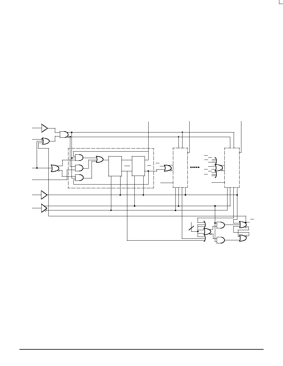
8-BIT BINARY COUNTER LOGIC DIAGRAM
Note that this diagram is provided for understanding of logic operation only.
It should not be used for propagation delays as many gate functions are achieved internally without incurring a full gate delay.
P1
SLAVE
MASTER
5
TC
Q1
Q0
P7
Q6
Q5
Q4
Q3
Q2
Q1
CE
Q0
BIT 1
CE
Q0
Q0M
Q0M
BIT 0
PE
TCLD
CE
PO
MR
CLK
BIT 7
BITS 2≠6
Q7

MC10E016 MC100E016
2≠3
MOTOROLA
ECLinPS and ECLinPS Lite
DL140 -- Rev 4
DC CHARACTERISTICS (VEE = VEE(min) to VEE(max); VCC = VCCO = GND)
0
∞
C
25
∞
C
85
∞
C
Symbol
Characteristic
min
typ
max
min
typ
max
min
typ
max
Unit
Condition
IIH
Input HIGH Current
150
150
150
µ
A
IEE
Power Supply Current
mA
10E
151
181
151
181
151
181
100E
151
181
151
181
174
208
AC CHARACTERISTICS (VEE = VEE(min) to VEE(max); VCC = VCCO = GND)
0
∞
C
25
∞
C
85
∞
C
Symbol
Characteristic
min
typ
max
min
typ
max
min
typ
max
Unit
Condition
fCOUNT
Max. Count Frequency
700
900
700
900
700
900
MHz
tPLH
Propagation Delay to Output
ps
tPHL
CLK to Q
600
725
1000
600
725
1000
600
725
1000
MR to Q
600
775
1000
600
775
1000
600
775
1000
CLK to TC
550
775
900
550
775
900
550
775
1050
MR to TC
625
775
1000
625
775
1000
625
775
1000
ts
Setup Time
ps
Pn
150
≠ 30
150
≠ 30
150
≠ 30
CE
600
400
600
400
600
400
PE
600
400
600
400
600
400
TCLD
500
300
500
300
500
300
th
Hold Time
Pn
350
100
350
100
350
100
CE
0
≠ 400
0
≠ 400
0
≠ 400
PE
0
≠ 400
0
≠ 400
0
≠ 400
TCLD
100
≠ 300
100
≠ 300
100
≠ 300
tRR
Reset Recovery Time
900
700
900
700
900
700
ps
tPW
Minimum Pulse Width
ps
CLK, MR
400
400
400
tr
Rise/Fall Times
ps
tf
20 - 80%
300
510
800
300
510
800
300
510

MC10E016 MC100E016
MOTOROLA
ECLinPS and ECLinPS Lite
DL140 -- Rev 4
2≠4
FUNCTION TABLE
Function
PE
CE
MR
TCLD
CLK
P7-P4
P3
P2
P1
P0
Q7-Q4
Q3
Q2
Q1
Q0
TC
Load
L
X
L
X
Z
H
H
H
L
L
H
H
H
L
L
H
Count
H
L
L
L
Z
X
X
X
X
X
H
H
H
L
H
H
H
L
L
L
Z
X
X
X
X
X
H
H
H
H
L
H
H
L
L
L
Z
X
X
X
X
X
H
H
H
H
H
L
H
L
L
L
Z
X
X
X
X
X
L
L
L
L
L
H
Load
L
X
L
X
Z
H
H
H
L
L
H
H
H
L
L
H
Hold
H
H
L
X
Z
X
X
X
X
X
H
H
H
L
L
H
H
H
L
X
Z
X
X
X
X
X
H
H
H
L
L
H
Load On
H
L
L
H
Z
H
L
H
H
L
H
H
H
L
H
H
Terminal
H
L
L
H
Z
H
L
H
H
L
H
H
H
H
L
H
Count
H
L
L
H
Z
H
L
H
H
L
H
H
H
H
H
L
H
L
L
H
Z
H
L
H
H
L
H
L
H
H
L
H
H
L
L
H
Z
H
L
H
H
L
H
L
H
H
H
H
H
L
L
H
Z
H
L
H
H
L
H
H
L
L
L
H
Reset
X
X
H
X
X
X
X
X
X
X
L
L
L
L
L
H
Applications Information
Cascading Multiple E016 Devices
For applications which call for larger than 8-bit counters
multiple E016s can be tied together to achieve very wide
bit width counters. The active low terminal count (TC)
output and count enable input (CE) greatly facilitate the
cascading of E016 devices. Two E016s can be cascaded
without the need for external gating, however for counters
wider than 16 bits external OR gates are necessary for
cascade implementations.
Figure 1 below pictorially illustrates the cascading of 4
E016s to build a 32-bit high frequency counter. Note the E101
gates used to OR the terminal count outputs of the lower order
E016s to control the counting operation of the higher order
bits. When the terminal count of the preceding device (or
devices) goes low (the counter reaches an all 1s state) the
more significant E016 is set in its count mode and will count
one binary digit upon the next positive clock transition. In
addition, the preceding devices will also count one bit thus
sending their terminal count outputs back to a high state
disabling the count operation of the more significant counters
and placing them back into hold modes. Therefore, for an
E016 in the chain to count, all of the lower order terminal count
outputs must be in the low state. The bit width of the counter
can be increased or decreased by simply adding or
subtracting E016 devices from Figure 1 and maintaining the
logic pattern illustrated in the same figure.
The maximum frequency of operation for the cascaded
counter chain is set by the propagation delay of the TC output
and the necessary setup time of the CE input and the
propagation delay through the OR gate controlling it (for 16-bit
counters the limitation is only the TC propagation delay and
the CE setup time). Figure 1 shows EL01 gates used to control
the count enable inputs, however, if the frequency of operation
is lower a slower, ECL OR gate can be used. Using the worst
case guarantees for these parameters from the ECLinPS data
book, the maximum count frequency for a greater than 16-bit
counter is 500MHz and that for a 16-bit counter is 625MHz.
Figure 1. 32-Bit Cascaded E016 Counter
EL01
CLOCK
P0 ≠> P7
TC
CLK
P0 ≠> P7
TC
CLK
EL01
P0 ≠> P7
TC
CLK
P0 ≠> P7
MSB
E016
PE
CE
Q0 ≠> Q7
Q0 ≠> Q7
Q0 ≠> Q7
E016
PE
CE
Q0 ≠> Q7
E016
PE
CE
LSB
E016
PE
CE
LO
LOAD
TC
CLK

MC10E016 MC100E016
2≠5
MOTOROLA
ECLinPS and ECLinPS Lite
DL140 -- Rev 4
Applications Information
(continued)
Note that this assumes the trace delay between the TC
outputs and the CE inputs are negligible. If this is not
the case estimates of these delays need to be added to
the calculations.
Programmable Divider
The E016 has been designed with a control pin which
makes it ideal for use as an 8-bit programmable divider. The
TCLD pin (load on terminal count) when asserted reloads the
data present at the parallel input pin (Pn's) upon reaching
terminal count (an all 1s state on the outputs). Because this
feedback is built internal to the chip, the programmable
division operation will run at very nearly the same frequency
as the maximum counting frequency of the device. Figure 2
below illustrates the input conditions necessary for utilizing the
E016 as a programmable divider set up to divide by 113.
H
L
H
H
L
L
L
H
H
H
H
TC
PE
CE
TCLD
CLK
P7
P6
P4
P3
P2
P1
P0
P5
Q7
Q6
Q4
Q3
Q2
Q1
Q0
Q5
Figure 2. Mod 2 to 256 Programmable Divider
To determine what value to load into the device to
accomplish the desired division, the designer simply subtracts
the binary equivalent of the desired divide ratio from the binary
value for 256. As an example for a divide ratio of 113:
Pn's = 256 ≠ 113 = 8F16 = 1000 1111
where:
P0 = LSB and P7 = MSB
Forcing this input condition as per the setup in Figure 2 will
result in the waveforms of Figure 3. Note that the TC output is
used as the divide output and the pulse duration is equal to a
Table 1. Preset Values for Various Divide Ratios
Divide
Ratio
Preset Data Inputs
Ratio
P7
P6
P5
P4
P3
P2
P1
P0
2
H
H
H
H
H
H
H
L
3
H
H
H
H
H
H
L
H
4
H
H
H
H
H
H
L
L
5
H
H
H
H
H
L
H
H
∑
∑
∑
∑
∑
∑
∑
∑
∑
∑
∑
∑
∑
∑
∑
∑
∑
∑
112
H
L
L
H
L
L
L
L
113
H
L
L
L
H
H
H
H
114
H
L
L
L
H
H
H
L
∑
∑
∑
∑
∑
∑
∑
∑
∑
∑
∑
∑
∑
∑
∑
∑
∑
∑
254
L
L
L
L
L
L
H
L
255
L
L
L
L
L
L
L
H
256
L
L
L
L
L
L
L
L
full clock period. For even divide ratios, twice the desired
divide ratio can be loaded into the E016 and the TC output can
feed the clock input of a toggle flip flop to create a signal
divided as desired with a 50% duty cycle.
A single E016 can be used to divide by any ratio from 2 to
256 inclusive. If divide ratios of greater than 256 are needed
multiple E016s can be cascaded in a manner similar to that
already discussed. When E016s are cascaded to build larger
dividers the TCLD pin will no longer provide a means for
loading on terminal count. Because one does not want to
reload the counters until all of the devices in the chain have
reached terminal count, external gating of the TC pins must be
used for multiple E016 divider chains.
∑∑∑
PE
∑∑∑
∑∑∑
Clock
TC
Load
DIVIDE BY 113
Load
1001 0000
1001 0001
1111 1100
1111 1101
1111 1110
1111 1111
Figure 3. Divide by 113 E016 Programmable Divider Waveforms