 | ÐлекÑÑоннÑй компоненÑ: MC1458D | СкаÑаÑÑ:  PDF PDF  ZIP ZIP |
Äîêóìåíòàöèÿ è îïèñàíèÿ www.docs.chipfind.ru

Device
Operating
Temperature Range
Package
MC1458, C
ORDERING INFORMATION
MC1458CD, D
MC1458CP1, P1
TA = 0
°
to +70
°
C
SO8
Plastic DIP
Order this document by MC1458/D
A
+
+
B
SEMICONDUCTOR
TECHNICAL DATA
DUAL
OPERATIONAL AMPLIFIERS
(DUAL MC1741)
P1 SUFFIX
PLASTIC PACKAGE
CASE 626
D SUFFIX
PLASTIC PACKAGE
CASE 751
(SO8)
1
1
8
8
Inputs
A
1
2
3
4
8
7
6
5
(Top View)
VEE
Output A
Output B
VCC
Inputs
B
PIN CONNECTIONS
1
MOTOROLA ANALOG IC DEVICE DATA
Internally Compensated,
High Performance
Dual Operational Amplifiers
The MC1458, C was designed for use as a summing amplifier, integrator,
or amplifier with operating characteristics as a function of the external
feedback components.
·
No Frequency Compensation Required
·
Short Circuit Protection
·
Wide Common Mode and Differential Voltage Ranges
·
Low Power Consumption
·
No LatchUp
MAXIMUM RATINGS
(TA = +25
°
C, unless otherwise noted.)
Rating
Symbol
Value
Unit
Power Supply Voltage
VCC
VEE
+18
18
Vdc
Input Differential Voltage
VID
±
30
V
Input Common Mode Voltage (Note 1)
VICM
±
15
V
Output Short Circuit Duration (Note 2)
tSC
Continuous
Operating Ambient Temperature Range
TA
0 to +70
°
C
Storage Temperature Range
Tstg
55 to +125
°
C
Junction Temperature
TJ
150
°
C
NOTES: 1. For supply voltages less than
±
15 V, the absolute maximum
input voltage is equal to the supply voltage.
2. Supply voltage equal to or less than 15 V.
Representative Schematic Diagram
Noninverting
Input
Inverting
Input
VCC
VEE
39 k
1.0 k
1.0 k
50 k
50 k
50
50
25
4.5 k
7.5 k
30 pF
Output
©
Motorola, Inc. 1996
Rev 1
MC1458, C
2
MOTOROLA ANALOG IC DEVICE DATA
ELECTRICAL CHARACTERISTICS
(VCC = +15 V, VEE = 15 V, TA = 25
°
C, unless otherwise noted. (Note 3))
Ch
i i
S
b l
MC1458
MC1458C
U i
Characteristic
Symbol
Min
Typ
Max
Min
Typ
Max
Unit
Input Offset Voltage (RS
10 k)
VIO
2.0
6.0
2.0
1.0
mV
Input Offset Current
IIO
20
200
20
300
nA
Input Bias Current
IIB
80
500
80
700
nA
Input Resistance
ri
0.3
2.0
2.0
M
Input Capacitance
Ci
1.4
1.4
pF
Offset Voltage Adjustment Range
VIOR
±
15
±
15
mV
Common Mode Input Voltage Range
VICR
±
12
±
13
±
11
±
13
V
Large Signal Voltage Gain
AVOL
V/mV
(VO =
±
10 V, RL = 2.0 k)
20
200
(VO =
±
10 V, RL = 10 k)
20
200
Output Resistance
ro
75
75
Common Mode Rejection (RS
10 k)
CMR
70
90
60
90
dB
Supply Voltage Rejection (RS
10 k)
PSR
30
150
30
µ
V/V
Output Voltage Swing
VO
V
(RS
10 k)
±
12
±
14
±
11
±
14
(RS
2.0 k)
±
10
±
13
±
9.0
±
13
Output Short Circuit Current
ISC
20
20
mA
Supply Currents (Both Amplifiers)
ID
2.3
5.6
2.3
8.0
mA
Power Consumption
PC
70
170
70
240
mW
Transient Response (Unity Gain)
(VI = 20 mV, RL
2.0 k
, CL
100 pF) Rise Time
tTLH
0.3
0.3
µ
s
(VI = 20 mV, RL
2.0 k
, CL
100 pF) Overshoot
os
15
15
%
(VI = 10 V, RL
2.0 k
, CL
100 pF) Slew Rate
SR
0.5
0.5
V/
µ
s
ELECTRICAL CHARACTERISTICS
(VCC = +15 V, VEE = 15 V, TA = Thigh to Tlow, unless otherwise noted. (Note 3))*
Ch
i i
S
b l
MC1458
MC1458C
U i
Characteristic
Symbol
Min
Typ
Max
Min
Typ
Max
Unit
Input Offset Voltage (RS
10 k
)
VIO
7.5
12
mV
Input Offset Current (TA = 0
°
to +70
°
C)
IIO
300
400
nA
Input Bias Current (TA = 0
°
to +70
°
C)
IIB
800
1000
nA
Output Voltage Swing
VO
V
(Rs
10 k)
±
12
±
14
(Rs
2 k)
±
10
±
13
±
9.0
±
13
Large Signal Voltage Gain
AVOL
V/mV
(VO =
±
10 V, RL = 2 k)
15
(VO =
±
10 V, RL = 10 k)
15
*Tlow = 0
°
C for MC1458, C
Thigh = +70
°
C for MC1458, C
NOTE:
3. Input pins of an unused amplifier must be grounded for split supply operation or biased at least 3.0 V above VEE for single supply operation.
MC1458, C
3
MOTOROLA ANALOG IC DEVICE DATA
Figure 1. Burst Noise versus Source Resistance
Figure 2. RMS Noise versus Source Resistance
Figure 3. Output Noise versus Source Resistance
Figure 4. Spectral Noise Density
Figure 5. Burst Noise Test Circuit
Unlike conventional peak reading or RMS meters, this system
was especially designed to provide the quick response time
essential to burst (popcorn) noise testing.
The test time employed is 10 sec and the 20
µ
V peak limit
refers to the operational amplifier input thus eliminating errors
in the closed loop gain factor of the operational amplifier .
RS, SOURCE RESISTANCE (
)
0
10
100
1000
10
100
1.0 k
10 k
100 k
1.0 M
BW = 1.0 Hz to 1.0 kHz
e
n
,
e
n
,
INPUT
NOISE (peak) (
V
)
µ
RS, SOURCE RESISTANCE (
)
0.1
1.0
10
100
10
100
1.0
10 k
100 k
1.0 M
BW = 1.0 Hz to 1.0 kHz
OUTPUT
NOISE (rms mV)
RS, SOURCE RESISTANCE (
)
0
0.1
1.0
10
10
100
1.0 k
10 k
100 k
1.0 M
AV = 1000
10
1.0
e
n
,
100
f, FREQUENCY (Hz)
10
100
1.0 k
100 k
10 k
140
120
100
80
40
20
0
60
AV = 10, RS = 100 k
INPUT
NOISE (
nV/
Hz
)
+
1.0 k
Operational Amplifier
Under Test
Low Pass Filter
1.0 Hz to 1.0 kHz
100 k
X 500
X 2
To Pass / Fail
Indicator
100 k
100 k
+
+
Positive
Threshold
Voltage
Negative
Threshold
Voltage
e
n
,
INPUT
NOISE (peak) (
V
)
µ
MC1458, C
4
MOTOROLA ANALOG IC DEVICE DATA
V
O
,
OUTPUT
VOL
T
AGE (V
)
pp
V
O
, OUTPUT
VOL
T
AGE SWING (V
pp
)
Figure 6. Power Bandwidth
(Large Signal Swing versus Frequency)
Figure 7. Open Loop Frequency Response
Figure 8. Positive Output Voltage Swing
versus Load Resistance
Figure 9. Negative Output Voltage Swing
versus Load Resistance
Figure 10. Output Voltage Swing versus
Load Resistance (Single Supply Operation)
Figure 11. Single Supply Inverting Amplifier
f, FREQUENCY (Hz)
10
100
1.0 k
100 k
10 k
28
24
20
16
8.0
4.0
0
12
f, FREQUENCY (Hz)
0
20
20
40
60
80
100
120
10
100
1.0 k
10 k
100 k
1.0 M
10 M
10
VOL
T
AGE GAIN (dB)
A
VOL
,
RL, LOAD RESISTANCE (
)
±
15 V Supplies
±
12 V
15
13
11
9.0
7.0
5.0
3.0
1.0
100
200
500 700 1.0 k
2.0 k
5.0 k 7.0 k 10 k
±
9.0 V
±
6.0 V
V
O
, OUTPUT
VOL
T
AGE SWING (V)
RL, LOAD RESISTANCE (
)
±
15 V Supplies
±
12 V
15
13
11
9.0
7.0
5.0
3.0
1.0
100
200
500 700 1.0 k
2.0 k
5.0 k 7.0 k 10 k
±
9.0 V
±
6.0 V
V
O
, OUTPUT
VOL
T
AGE SWING (V)
+27 V
+24 V
+21 V
+18 V
+15 V
+12 V
+9.0 V
+6.0 V
+5.0 V
+30 V Supply
28
24
20
16
12
8.0
4.0
0
0
1.0
2.0
3.0
4.0
5.0
6.0
7.0
8.0
9.0
10
RL, LOAD RESISTANCE (k
)
100
µ
F
RL
VCC
200 k
50 k
+
Vin
7
4
2
3
10 k
MC1558
1.0 k
200 k
50 k
100
µ
F
(Voltage Follower)
THD < 5%
MC1458, C
5
MOTOROLA ANALOG IC DEVICE DATA
Figure 12. Noninverting Pulse Response
Figure 13. Transient Response Test Circuit
Figure 14. Unused OpAmp
5.0 V/DIV
10
µ
s/DIV
Output
Input
+
RL
CL
To Scope
(Input)
To Scope
(Output)
70
75
80
90
95
100
105
85
0
2.0
4.0
6.0
8.0
10
12
14
16
18
20
VCC, |VEE|, SUPPLY VOLTAGES (V)
A
V
,
VOL
T
AGE GAIN (dB)
Figure 15. Open Loop Voltage Gain
versus Supply Voltage
+
MC1458, C
6
MOTOROLA ANALOG IC DEVICE DATA
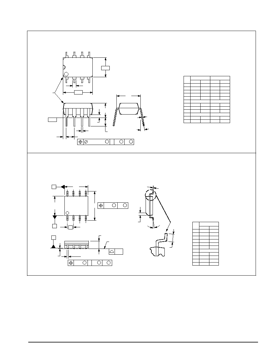
OUTLINE DIMENSIONS
NOTES:
1. DIMENSION L TO CENTER OF LEAD WHEN
FORMED PARALLEL.
2. PACKAGE CONTOUR OPTIONAL (ROUND OR
SQUARE CORNERS).
3. DIMENSIONING AND TOLERANCING PER ANSI
Y14.5M, 1982.
1
4
5
8
F
NOTE 2
A
B
T
SEATING
PLANE
H
J
G
D
K
N
C
L
M
M
A
M
0.13 (0.005)
B
M
T
DIM
MIN
MAX
MIN
MAX
INCHES
MILLIMETERS
A
9.40
10.16
0.370
0.400
B
6.10
6.60
0.240
0.260
C
3.94
4.45
0.155
0.175
D
0.38
0.51
0.015
0.020
F
1.02
1.78
0.040
0.070
G
2.54 BSC
0.100 BSC
H
0.76
1.27
0.030
0.050
J
0.20
0.30
0.008
0.012
K
2.92
3.43
0.115
0.135
L
7.62 BSC
0.300 BSC
M
10
10
N
0.76
1.01
0.030
0.040
_
_
P1 SUFFIX
PLASTIC PACKAGE
CASE 62605
ISSUE K
D SUFFIX
PLASTIC PACKAGE
CASE 75105
(SO8)
ISSUE R
SEATING
PLANE
1
4
5
8
A
0.25
M
C B
S
S
0.25
M
B
M
h
q
C
X 45
_
L
DIM
MIN
MAX
MILLIMETERS
A
1.35
1.75
A1
0.10
0.25
B
0.35
0.49
C
0.18
0.25
D
4.80
5.00
E
1.27 BSC
e
3.80
4.00
H
5.80
6.20
h
0
7
L
0.40
1.25
q
0.25
0.50
_
_
NOTES:
1. DIMENSIONING AND TOLERANCING PER ASME
Y14.5M, 1994.
2. DIMENSIONS ARE IN MILLIMETERS.
3. DIMENSION D AND E DO NOT INCLUDE MOLD
PROTRUSION.
4. MAXIMUM MOLD PROTRUSION 0.15 PER SIDE.
5. DIMENSION B DOES NOT INCLUDE MOLD
PROTRUSION. ALLOWABLE DAMBAR
PROTRUSION SHALL BE 0.127 TOTAL IN EXCESS
OF THE B DIMENSION AT MAXIMUM MATERIAL
CONDITION.
D
E
H
A
B
e
B
A1
C
A
0.10

MC1458, C
7
MOTOROLA ANALOG IC DEVICE DATA
Motorola reserves the right to make changes without further notice to any products herein. Motorola makes no warranty, representation or guarantee regarding
the suitability of its products for any particular purpose, nor does Motorola assume any liability arising out of the application or use of any product or circuit, and
specifically disclaims any and all liability, including without limitation consequential or incidental damages. "Typical" parameters which may be provided in Motorola
data sheets and/or specifications can and do vary in different applications and actual performance may vary over time. All operating parameters, including "Typicals"
must be validated for each customer application by customer's technical experts. Motorola does not convey any license under its patent rights nor the rights of
others. Motorola products are not designed, intended, or authorized for use as components in systems intended for surgical implant into the body, or other
applications intended to support or sustain life, or for any other application in which the failure of the Motorola product could create a situation where personal injury
or death may occur. Should Buyer purchase or use Motorola products for any such unintended or unauthorized application, Buyer shall indemnify and hold Motorola
and its officers, employees, subsidiaries, affiliates, and distributors harmless against all claims, costs, damages, and expenses, and reasonable attorney fees
arising out of, directly or indirectly, any claim of personal injury or death associated with such unintended or unauthorized use, even if such claim alleges that
Motorola was negligent regarding the design or manufacture of the part. Motorola and are registered trademarks of Motorola, Inc. Motorola, Inc. is an Equal
Opportunity/Affirmative Action Employer.

MC1458, C
8
MOTOROLA ANALOG IC DEVICE DATA
How to reach us:
USA / EUROPE / Locations Not Listed: Motorola Literature Distribution;
JAPAN: Nippon Motorola Ltd.; TatsumiSPDJLDC, 6F SeibuButsuryuCenter,
P.O. Box 20912; Phoenix, Arizona 85036. 18004412447 or 6023035454
3142 Tatsumi KotoKu, Tokyo 135, Japan. 038135218315
MFAX: RMFAX0@email.sps.mot.com TOUCHTONE 6022446609
ASIA/PACIFIC: Motorola Semiconductors H.K. Ltd.; 8B Tai Ping Industrial Park,
INTERNET: http://DesignNET.com
51 Ting Kok Road, Tai Po, N.T., Hong Kong. 85226629298
MC1458/D
*MC1458/D*