 | ÐлекÑÑоннÑй компоненÑ: MC33076P1 | СкаÑаÑÑ:  PDF PDF  ZIP ZIP |
Äîêóìåíòàöèÿ è îïèñàíèÿ www.docs.chipfind.ru
MC33076
SEMICONDUCTOR
TECHNICAL DATA
DUAL HIGH OUTPUT
CURRENT OPERATIONAL
AMPLIFIER
Order this document by MC33076/D
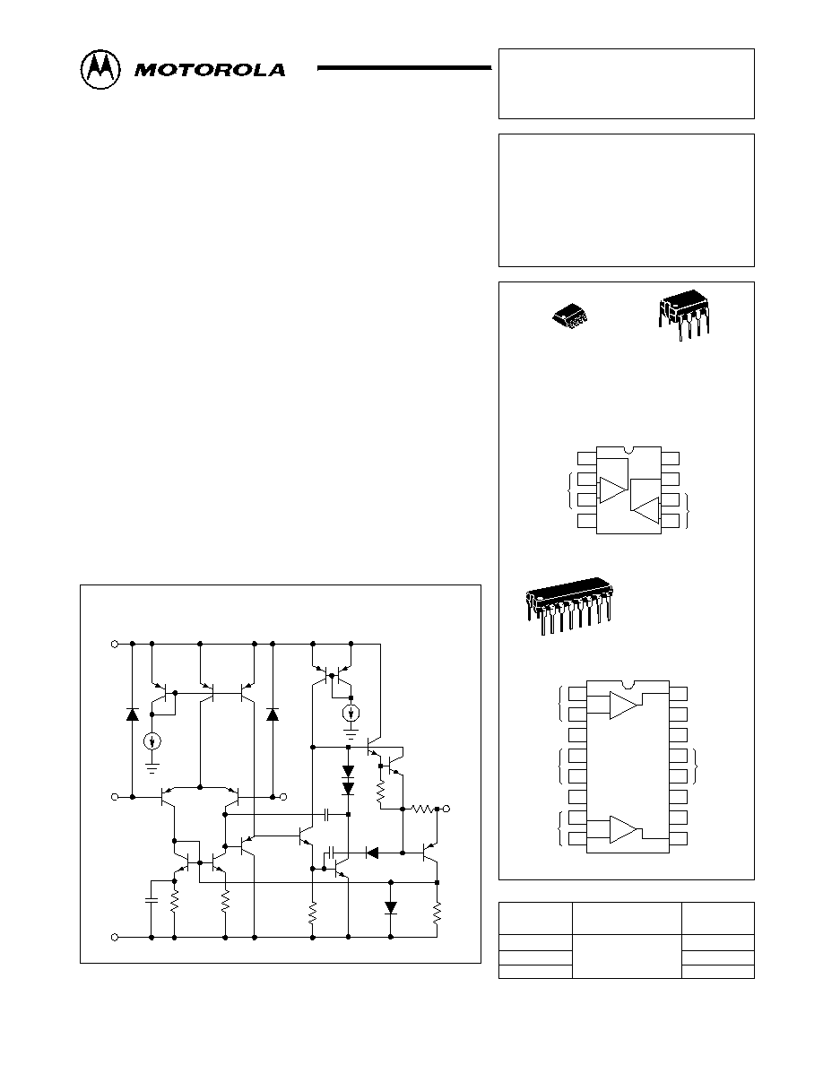
PIN CONNECTIONS
(8 Pin Pkg, Top View)
D SUFFIX
PLASTIC PACKAGE
CASE 751
(SO8)
16
15
14
13
12
11
10
9
Inputs 1
1
2
3
4
5
6
7
8
NC
NC
VEE
Inputs 2
Output 1
NC
VCC
VEE
NC
NC
Output 2
PIN CONNECTIONS
(16 Pin Pkg, Top View)
+
2
+
1
8
1
8
1
P1 SUFFIX
PLASTIC PACKAGE
CASE 626
16
1
P2 SUFFIX
PLASTIC PACKAGE
CASE 648C
DIP (12+2+2)
8
7
6
5
Inputs 1
1
2
3
4
Output 1
VEE
Output 2
VCC
Inputs 2
+ 1
+
2
ORDERING INFORMATION
Device
Operating
Temperature Range
Package
MC33076D
TA = 40
°
to + 85
°
C
SO8
MC33076P1
Plastic DIP
MC33076P2
Power Plastic
1
MOTOROLA ANALOG IC DEVICE DATA
Dual High Output Current,
Low Power, Low Noise
Bipolar Operational Amplifier
The MC33076 operational amplifier employs bipolar technology with
innovative high performance concepts for audio and industrial applications.
This device uses high frequency PNP input transistors to improve frequency
response. In addition, the amplifier provides high output current drive
capability while minimizing the drain current. The all NPN output stage
exhibits no deadband crossover distortion, large output voltage swing,
excellent phase and gain margins, low open loop high frequency output
impedance and symmetrical source and sink AC frequency performance.
The MC33076 is tested over the automotive temperature range and is
available in an 8pin SOIC package (D suffix) and in both the standard 8 pin
DIP and 16pin DIP packages for high power applications.
·
100
Output Drive Capability
·
Large Output Voltage Swing
·
Low Total Harmonic Distortion
·
High Gain Bandwidth: 7.4 MHz
·
High Slew Rate: 2.6 V/
µ
s
·
Dual Supply Operation:
±
2.0 V to
±
18 V
·
High Output Current: ISC = 250 mA typ
·
Similar Performance to MC33178
Equivalent Circuit Schematic
(Each Amplifier)
Vin+
VCC
Vin
VEE
Iref
Iref
CC
CM
Vout
©
Motorola, Inc. 1996
Rev 0
MC33076
2
MOTOROLA ANALOG IC DEVICE DATA
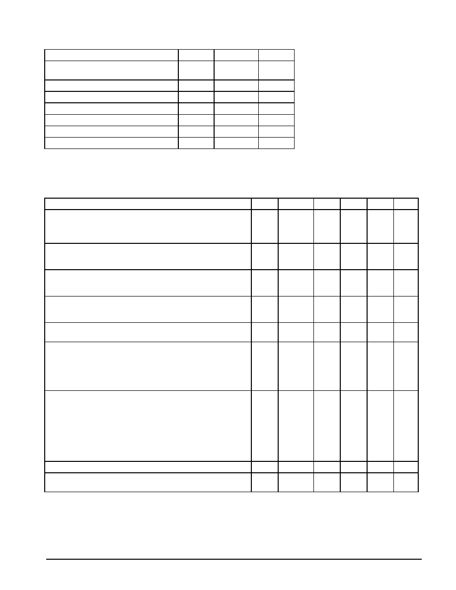
MAXIMUM RATINGS
Rating
Symbol
Value
Unit
Power Supply Voltage (Note 2)
VCC to
VEE
+36
V
Input Differential Voltage Range
VIDR
(Note 1)
V
Input Voltage Range
VIR
(Note 1)
V
Output Short Circuit Duration (Note 2)
tSC
5.0
sec
Maximum Junction Temperature
TJ
+150
°
C
Storage Temperature
Tstg
60 to +150
°
C
Maximum Power Dissipation
PD
(Note 2)
mW
NOTES: 1. Either or both input voltages should not exceed VCC or VEE.
2. Power dissipation must be considered to ensure maximum junction temperature (TJ)
is not exceeded (see power dissipation performance characteristic, Figure 1).
See applications section for further information.
DC ELECTRICAL CHARACTERICISTICS
(VCC = +15 V, VEE = 15 V, TA = 25
°
C, unless otherwise noted.)
Characteristics
Figure
Symbol
Min
Typ
Max
Unit
Input Offset Voltage (RS = 50
, VCM = 0 V)
(VS =
±
2.5 V to
±
15 V)
TA = +25
°
C
TA = 40
°
to +85
°
C
2
|VIO|
--
--
0.5
0.5
4.0
5.0
mV
Input Offset Voltage Temperature Coefficient
(RS = 50
, VCM = 0 V)
TA = 40
°
to +85
°
C
VIO/
T
--
2.0
--
µ
V/
°
C
Input Bias Current (VCM = 0 V)
TA = +25
°
C
TA = 40
°
to +85
°
C
3, 4
IIB
--
--
100
--
500
600
nA
Input Offset Current (VCM = 0 V)
TA = +25
°
C
TA = 40
°
to +85
°
C
|IIO|
--
--
5.0
--
70
100
nA
Common Mode Input Voltage Range
5
VICR
13
14
+14
13
V
Large Signal Voltage Gain (VO = 10 V to +10 V)
(TA = +25
°
C)
RL = 100
RL = 600
(TA = 40
°
to +85
°
C)
RL = 600
6
AVOL
25
50
25
--
200
--
--
--
--
kV/V
Output Voltage Swing (VID =
±
1.0 V)
(VCC = +15 V, VEE = 15 V)
RL = 100
RL = 100
RL = 600
RL = 600
(VCC = +2.5 V, VEE = 2.5 V)
RL = 100
RL = 100
7, 8, 9
VO+
VO
VO+
VO
VO+
VO
10
--
13
--
1.2
--
+11.7
11.7
+13.8
13.8
+1.66
1.74
--
10
--
13
--
1.2
V
Common Mode Rejection (Vin =
±
13 V)
10
CMR
80
116
--
dB
Power Supply Rejection
(VCC/VEE = +15 V/15 V, +5.0 V/15 V, +15 V/5.0 V)
11
PSR
80
120
--
dB
MC33076
3
MOTOROLA ANALOG IC DEVICE DATA
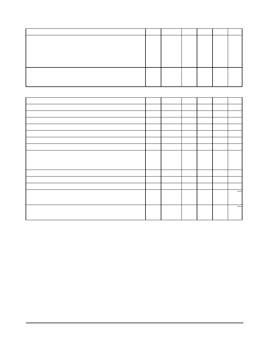
DC ELECTRICAL CHARACTERICISTICS
(VCC = +15 V, VEE = 15 V, TA = 25
°
C, unless otherwise noted.)
Characteristics
Figure
Symbol
Min
Typ
Max
Unit
Output Short Circuit Current (VID =
±
1.0 V Output to Gnd)
(VCC = +15 V, VEE = 15 V)
Source
Sink
(VCC = +2.5 V, VEE = 2.5 V)
Source
Sink
12, 13
ISC
190
--
63
--
+250
280
+94
80
--
215
--
46
mA
Power Supply Current per Amplifier (VO = 0 V)
(VS =
±
2.5 V to
±
15 V)
TA = +25
°
C
TA = 40
°
to +85
°
C
14
ID
--
--
2.2
--
2.8
3.3
mA
AC ELECTRICAL CHARACTERICISTICS
(VCC = +15 V, VEE = 15 V, TA = 25
°
C, unless otherwise noted.)
Characteristics
Figure
Symbol
Min
Typ
Max
Unit
Slew Rate (Vin = 10 V to +10 V, RL = 100
, CL = 100 pF, AV = +1)
15
SR
1.2
2.6
--
V/
µ
s
Gain Bandwidth Product (f = 20 kHz)
16
GBW
4.0
7.4
--
MHz
Unity Gain Frequency (Open Loop) (RL = 600
, CL = 0 pF)
--
fU
--
3.5
--
MHz
Gain Margin (RL = 600
, CL = 0 pF)
19, 20
Am
--
15
--
dB
Phase Margin (RL = 600
, CL = 0 pF)
19, 20
m
--
52
--
Deg
Channel Separation (f = 100 Hz to 20 kHz)
21
CS
--
120
--
dB
Power Bandwidth (VO = 20 Vpp, RL = 600
, THD
1%)
--
BWp
--
32
--
kHz
Total Harmonic Distortion (RL = 600
, VO = 2.0 Vpp, AV = +1)
f = 1.0 kHz
f = 10 kHz
f = 20 kHz
22
THD
--
--
--
0.0027
0.011
0.022
--
--
--
%
Open Loop Output Impedance (VO = 0 V, f = 2.5 MHz, AV = 10)
23
|ZO|
--
75
--
Differential Input Resistance (VCM = 0 V)
--
Rin
--
200
--
k
Differential Input Capacitance (VCM = 0 V)
--
Cin
--
10
--
pF
Equivalent Input Noise Voltage (RS = 100
)
f = 10 Hz
f = 1.0 kHz
24
en
--
--
7.5
5.0
--
nV/
Hz
Equivalent Input Noise Current
f = 10 Hz
f = 1.0 kHz
--
in
--
--
0.33
0.15
--
--
pA/
Hz
MC33076
4
MOTOROLA ANALOG IC DEVICE DATA
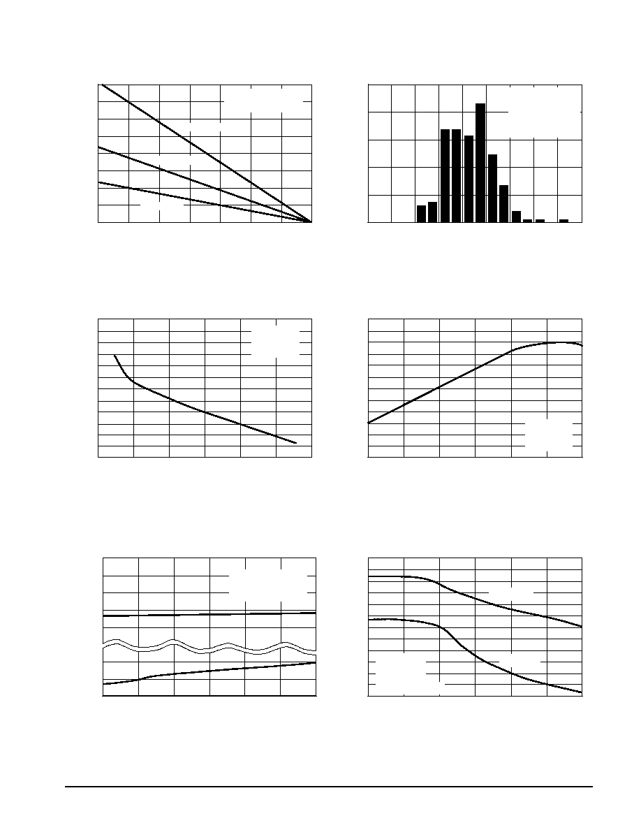
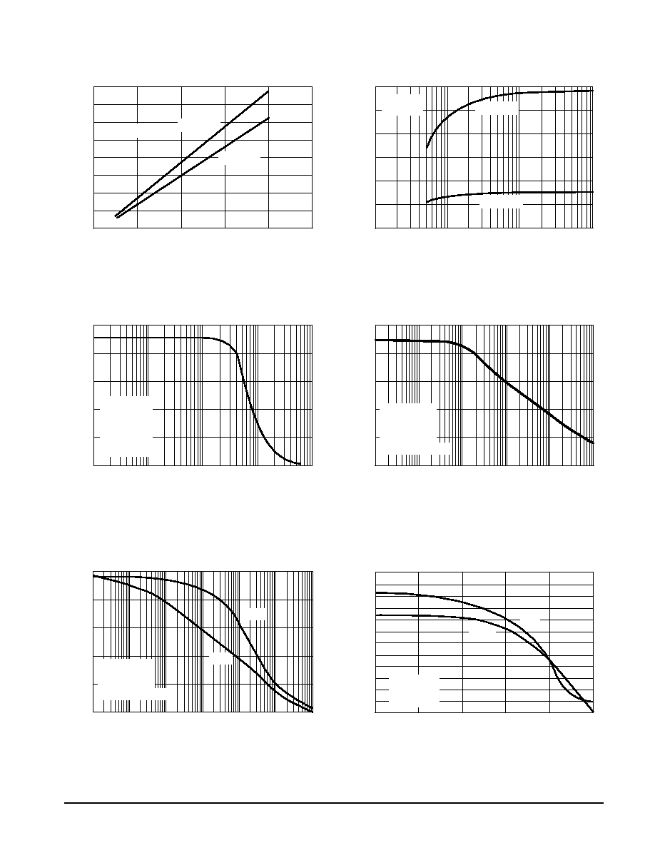
Figure 1. Maximum Power Dissipation
versus Temperature
, MAXIMUM POWER DISSIP
A
TION (mW)
60
30
TA, AMBIENT TEMPERATURE (
°
C)
MC33076P2
MC33076P1
MC33076D
See Application Section
for Further Information
PERCENT
AGE OF
AMPLIFIERS
(%)
Figure 2. Distribution of Input
Offset Voltage
VIO, INPUT OFFSET VOLTAGE (mV)
Figure 3. Input Bias Current versus
Common Mode Voltage
VCM, COMMON MODE VOLTAGE (V)
I , INPUT
BIAS
CURRENT
(nA)
IB
I , INPUT
BIAS
CURRENT
(nA)
IB
Figure 4. Input Bias Current
versus Temperature
TA, AMBIENT TEMPERATURE (
°
C)
A
Figure 5. Input Common Mode Voltage
Range versus Temperature
TA, TEMPERATURE (
°
C)
Figure 6. Open Loop Voltage Gain
versus Temperature
TA, AMBIENT TEMPERATURE (
°
C)
P
D
VOL
, OPEN LOOP
VOL
T
AGE GAIN (dB)
4000
3500
3000
2500
2000
1500
1000
500
0
25
20
15
10
5
0
250
225
200
175
150
125
100
150
137
125
112
100
88
75
VEE
120
115
110
105
100
95
90
VCC1.0
VEE+0.125
VEE+0.25
VCC0.75
VCC0.50
VCC0.25
VCC
0
30
60
90
120
150
2.0
1.5
1.0
0.5
0
0.5
1.0
1.5
2.0
15
10
5.0
0
5.0
10
15
55
25
5.0
35
65
95
125
55
25
5.0
35
65
95
125
55
25
5.0
35
65
95
125
2.5
180 amplifiers tested
from 3 wafer lots
VCC =
±
15 V
TA = 25
°
C
(Plastic DIP package)
VCC = +15 V
VEE = 15 V
TA = 25
°
C
VCC = +15 V
VEE = 15 V
VCM = 0 V
VCC = + 5.0 V to +18 V
VEE = 5.0 V to 18 V
VIO = 5.0 mV
RL = 2.0 k
RL = 100
VCC = +15 V
VEE = 15 V
f = 10 Hz
VO = 10 to +10 V
MC33076
5
MOTOROLA ANALOG IC DEVICE DATA
V
O
,
OUTPUT
VOL
T
AGE (V
)
pp
V
O
,
OUTPUT
VOL
T
AGE (V
)
pp
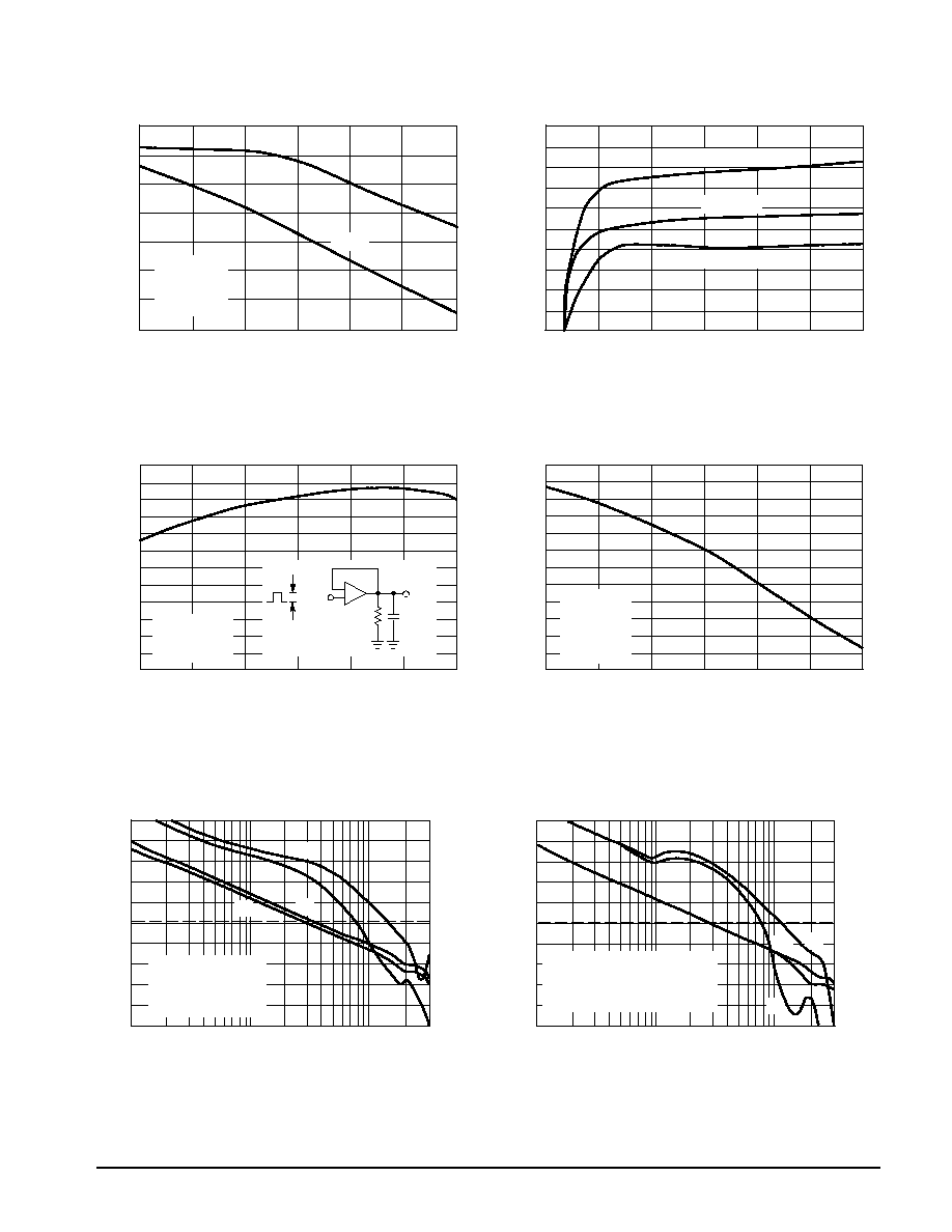
Figure 7. Output Voltage Swing
versus Supply Voltage
VCC, |VEE|, SUPPLY VOLTAGE (V)
Figure 8. Maximum PeaktoPeak Output
Voltage Swing versus Load Resistance
RL, LOAD RESISTANCE TO GROUND (
)
Figure 9. Output Voltage
versus Frequency
f, FREQUENCY (Hz)
CMR, COMMON MODE REJECTION (dB)
Figure 10. Common Mode Rejection
versus Frequency Over Temperature
f, FREQUENCY (Hz)
|I
Figure 11. Power Supply Rejection
versus Frequency Over Temperature
Figure 12. Output Short Circuit Current
versus Output Voltage
|VO|, OUTPUT VOLTAGE (V)
PSR, POWER SUPPL
Y
REJECTION (dB)
f, FREQUENCY (Hz)
15
V
O
,
OUTPUT
VOL
T
AGE SWING (Vpp)
SC
|, OUTPUT
SHOR
T
CIRCUIT
CURRENT
(mA)
40
35
30
25
20
15
10
5.0
0
25
20
15
10
5.0
0
30
25
20
15
10
5.0
0
100
80
60
40
20
0
100
80
60
40
20
0
300
250
200
150
100
50
RL = 100
RL = 10 k
TA = 25
°
C
100
1.0 k
10 k
100 k
1.0 M
10
0
5.0
10
15
20
25
10
100
1.0 k
10 k
100
1.0 k
10 k
100 k
1.0 M
100
1.0 k
10 k
100 k
1.0 M
10
10 M
0
3.0
6.0
9.0
12
0
VS =
±
15 V
VS =
±
5.0 V
TA = 25
°
C
f = 1.0 kHz
VCC = +15 V
VEE = 15 V
RL = 100
AV = +1.0
THD =
1.0%
TA = 25
°
C
VCC = +15 V
VEE = 15 V
VCM = 0 V
VCM =
±
1.5 V
TA = 55
°
to +125
°
C
+PSR
PSR
VCC = +15 V
VEE = 15 V
VCC =
±
1.5 V
TA = 55
°
to +125
°
C
Source
Sink
VCC = +15 V
VEE = 15 V
VID =
±
1.0 V
MC33076
6
MOTOROLA ANALOG IC DEVICE DATA
1
A
2
A
1B
2B
|, OUTPUT
SHOR
T
CIRCUIT
CURRENT
(mA)
I
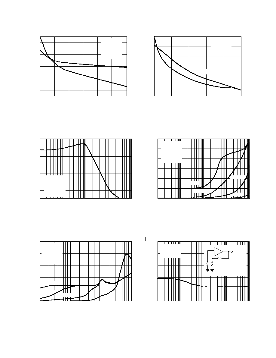
Figure 13. Output Short Circuit Current
versus Temperature
VCC |VEE|, SUPPLY VOLTAGE (V)
Figure 14. Supply Current versus
Supply Voltage with No Load
TA, AMBIENT TEMPERATURE (
°
C)
Figure 15. Slew Rate
versus Temperature
SR, SLEW RA
TE (V/
GBW
, GAIN BANDWIDTH PRODUCT
(MHz)
Figure 16. Gain Bandwidth Product
versus Temperature
TA, AMBIENT TEMPERATURE (
°
C)
Figure 17. Voltage Gain and Phase
versus Frequency
f, FREQUENCY (Hz)
Figure 18. Voltage Gain and Phase
versus Frequency
TA, AMBIENT TEMPERATURE (
°
C)
Vin
100
100pF
80
120
160
200
240
280
, EXCESS PHASE (DEGREES)
A
, EXCESS PHASE (DEGREES)
f, FREQEUNCY (Hz)
80
120
160
200
280
+
240
|I
SC
µ
S)
V
,
VOL
T
AGE GAIN (dB)
A
V
,
VOL
T
AGE GAIN (dB)
D
,
SUPPL
Y
CURRENT/AMPLIFIER (mA)
5.0
4.0
3.0
2.0
1.0
0
320
300
280
260
240
220
200
180
8.5
8.0
7.5
7.0
6.5
6.0
5.5
3.0
2.5
2.0
1.5
1.0
0.5
0
50
30
10
10
30
50
50
30
10
10
30
50
0
3.0
6.0
9.0
12
15
18
55
25
5.0
35
65
95
125
55
25
5.0
35
65
95
125
30 M
55
25
5.0
35
65
95
125
10 M
1.0 M
100 k
30 M
10 M
1.0 M
100 k
Source
Sink
VCC = +15 V
VEE = 15 V
VID =
±
1.0 V
RL < 10
TA = + 25
°
C
TA = +125
°
C
TA = 55
°
C
VCC = +15 V
VEE = 15 V
Vin = 20 Vpp
VCC = +15 V
VEE = 15 V
f = 100 Hz
RL = 100
CL = 0 pF
1
A
2
A
1
B
2
B
1A) Phase, VS =
±
18 V
2A) Phase, VS =
±
1.5 V
1B) Gain, VS =
±
18 V
2B) Gain, VS =
±
1.5 V
1A) Phase, (R = 100
)
2A) Phase, (R = 100
, C = 300 pF)
1B) Gain, (R = 100
)
2B) Gain, (R = 100
, C = 300 pF)
MC33076
7
MOTOROLA ANALOG IC DEVICE DATA
AV = +1000
AV = +100
AV = +10
AV = +1
Figure 19. Phase Margin and Gain Margin
versus Differential Source Resistance
CL, OUTPUT LOAD CAPACITANCE (pF)
Figure 20. Open Loop Gain Margin and Phase
Margin versus Output Load Capacitance
A
RT, DIFFERENTIAL SOURCE RESISTANCE (
)
Figure 21. Channel Separation
versus Frequency
CS, CHANNEL
SEP
ARA
TION
(dB)
f, FREQUENCY (Hz)
m
50
40
30
20
10
0
16
14
12
10
8.0
6.0
4.0
2.0
0
THD,
T
O
T
A
L
HARMONIC DIST
OR
TION (%)
f, FREQUENCY (Hz)
Figure 22. Total Harmonic Distortion
versus Frequency
m
, GAIN MARGIN (dB)
, PHASE MARGIN (DEGREES)
A
m
, OPEN LOOP
GAIN MARGIN (dB)
m
, PHASE MARGIN (DEGREES)
Figure 23. Output Impedance
versus Frequency
f, FREQUENCY (Hz)
Z
O
,
OUTPUT
IMPEDANCE (
)
Figure 24. Input Referred Noise Voltage
versus Frequency
e
f, FREQUENCY (Hz)
Hz)
n
, INPUT
REFERRED NOISE VOL
T
AGE (NV/
AV = 1000
AV = 100
AV = 10
AV = 1.0
60
50
40
30
20
10
20
16
12
8.0
4.0
0
130
120
110
100
90
80
0
140
70
3.0
2.5
2.0
1.5
1.0
0.5
0
100
80
60
40
20
0
20
16
12
8.0
4.0
0
0
400
800
1200
1600
2000
0
2.0 k
4.0 k
6.0 k
8.0 k
10 k
12 k
100
1.0 k
10 k
100 k
1.0 M
10
100
1.0 k
10 k
100 k
10 M
1.0 M
100 k
10 k
10
100
1.0 k
10 k
100 k
Gain Margin
VCC = +15 V
VEE = 15 V
RT = R1 + R2
VO = 0 V
TA = 25
°
C
Phase Margin
Phase Margin
Gain Margin
VCC = +15 V
VEE = 15 V
VO = 0 V
Drive Channel
VCC = +15 V
VEE = 15 V
RL = 100
TA = 25
°
C
VCC = +15 V
VEE = 15 V
VCM = 0 V
VO = 0 V
TA = 25
°
C
VCC = +15 V
VEE = 15 V
TA = 25
°
C
VO
+
Input Noise Voltage
Test Circuit
VCC = +15 V
VEE = 15 V
RL = 100
VO = 2.0 Vpp
TA = 25
°
C
MC33076
8
MOTOROLA ANALOG IC DEVICE DATA
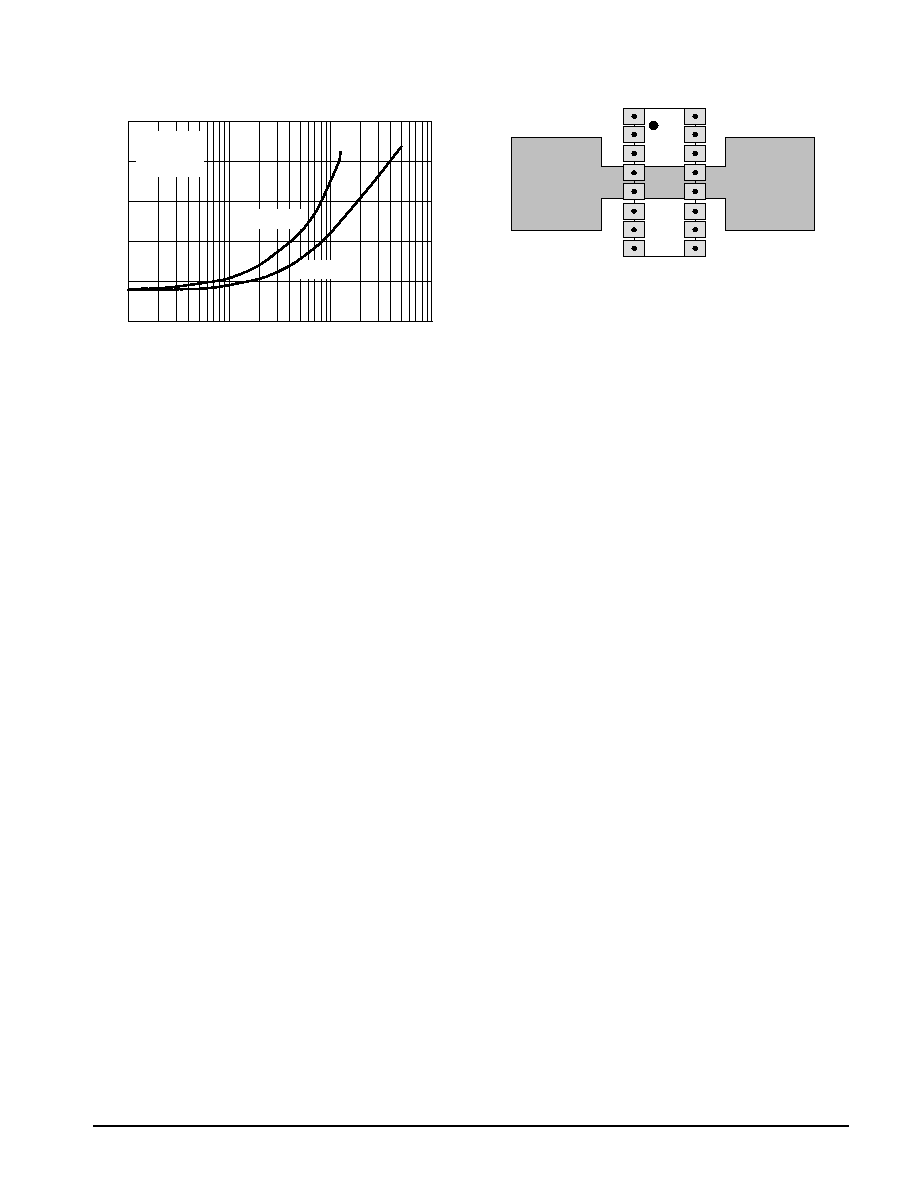
Figure 25. Percent Overshoot
versus Load Capacitance
CL, LOAD CAPACITANCE (pF)
os, PERCENT
OVERSHOOT
(%)
10 k
1000
100
10
100
80
60
40
20
0
RL = 100
RL = 2.0 k
VCC = +15 V
VEE = 15 V
TA = 25
°
C
Figure 26. PC Board Heatsink Example
Copper
Pad
Copper
Pad
APPLICATIONS INFORMATION
The MC33076 dual operational amplifier is available in the
standard 8pin plastic dualinline (DIP) and surface mount
packages, and also in a 16pin batwing power package. To
enhance the power dissipation capability of the power
package, Pins 4, 5, 12, and 13 are tied together on the
leadframe, giving it an ambient thermal resistance of 52
°
C/W
typically, in still air. The junctiontoambient thermal
resistance (R
JA) can be decreased further by using a copper
padb on the printed circuit board (as shown in Figure 26) to
draw the heat away from the package.
Care must be taken
not to exceed the maximum junction temperature or damage
to the device may occur.
MC33076
9
MOTOROLA ANALOG IC DEVICE DATA
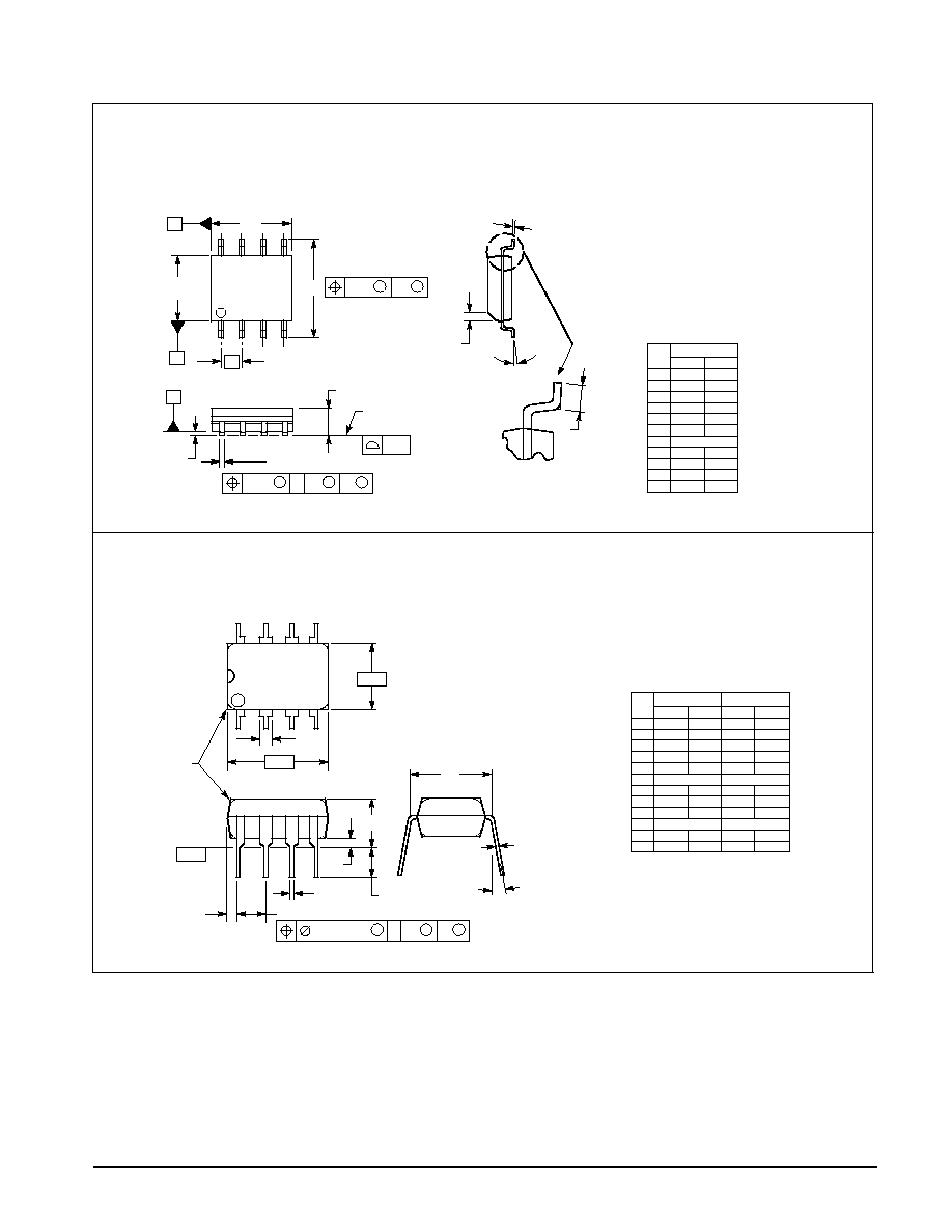
OUTLINE DIMENSIONS
D SUFFIX
PLASTIC PACKAGE
CASE 75105
(SO8)
ISSUE R
P1 SUFFIX
PLASTIC PACKAGE
CASE 62605
ISSUE K
NOTES:
1. DIMENSION L TO CENTER OF LEAD WHEN
FORMED PARALLEL.
2. PACKAGE CONTOUR OPTIONAL (ROUND OR
SQUARE CORNERS).
3. DIMENSIONING AND TOLERANCING PER ANSI
Y14.5M, 1982.
1
4
5
8
F
NOTE 2
A
B
T
SEATING
PLANE
H
J
G
D
K
N
C
L
M
M
A
M
0.13 (0.005)
B
M
T
DIM
MIN
MAX
MIN
MAX
INCHES
MILLIMETERS
A
9.40
10.16
0.370
0.400
B
6.10
6.60
0.240
0.260
C
3.94
4.45
0.155
0.175
D
0.38
0.51
0.015
0.020
F
1.02
1.78
0.040
0.070
G
2.54 BSC
0.100 BSC
H
0.76
1.27
0.030
0.050
J
0.20
0.30
0.008
0.012
K
2.92
3.43
0.115
0.135
L
7.62 BSC
0.300 BSC
M
10
10
N
0.76
1.01
0.030
0.040
_
_
SEATING
PLANE
1
4
5
8
A
0.25
M
C B
S
S
0.25
M
B
M
h
q
C
X 45
_
L
DIM
MIN
MAX
MILLIMETERS
A
1.35
1.75
A1
0.10
0.25
B
0.35
0.49
C
0.18
0.25
D
4.80
5.00
E
1.27 BSC
e
3.80
4.00
H
5.80
6.20
h
0
7
L
0.40
1.25
q
0.25
0.50
_
_
NOTES:
1. DIMENSIONING AND TOLERANCING PER ASME
Y14.5M, 1994.
2. DIMENSIONS ARE IN MILLIMETERS.
3. DIMENSION D AND E DO NOT INCLUDE MOLD
PROTRUSION.
4. MAXIMUM MOLD PROTRUSION 0.15 PER SIDE.
5. DIMENSION B DOES NOT INCLUDE MOLD
PROTRUSION. ALLOWABLE DAMBAR
PROTRUSION SHALL BE 0.127 TOTAL IN EXCESS
OF THE B DIMENSION AT MAXIMUM MATERIAL
CONDITION.
D
E
H
A
B
e
B
A1
C
A
0.10
MC33076
10
MOTOROLA ANALOG IC DEVICE DATA
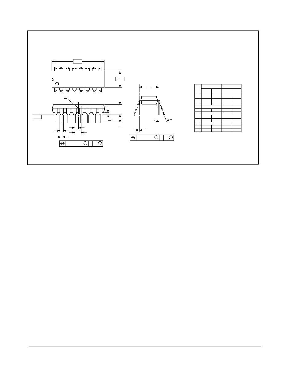
OUTLINE DIMENSIONS
P2 SUFFIX
PLASTIC PACKAGE
CASE 648C03
(DIP (12+2+2))
ISSUE C
DIM
MIN
MAX
MIN
MAX
MILLIMETERS
INCHES
A
0.740
0.840
18.80
21.34
B
0.240
0.260
6.10
6.60
C
0.145
0.185
3.69
4.69
D
0.015
0.021
0.38
0.53
E
0.050 BSC
1.27 BSC
F
0.040
0.70
1.02
1.78
G
0.100 BSC
2.54 BSC
J
0.008
0.015
0.20
0.38
K
0.115
0.135
2.92
3.43
L
0.300 BSC
7.62 BSC
M
0
10
0
10
N
0.015
0.040
0.39
1.01
_
_
_
_
NOTES:
1. DIMENSIONING AND TOLERANCING PER ANSI
Y14.5M, 1982.
2. CONTROLLING DIMENSION: INCH.
3. DIMENSION L TO CENTER OF LEADS WHEN
FORMED PARALLEL.
4. DIMENSION B DOES NOT INCLUDE MOLD FLASH.
5. INTERNAL LEAD CONNECTION BETWEEN 4 AND
5, 12 AND 13.
A
B
16
9
1
8
F
D
G
E
N
C
NOTE 5
16 PL
S
A
M
0.13 (0.005)
T
T
SEATING
PLANE
S
B
M
0.13 (0.005)
T
J
16 PL
M
L

MC33076
11
MOTOROLA ANALOG IC DEVICE DATA
Motorola reserves the right to make changes without further notice to any products herein. Motorola makes no warranty, representation or guarantee regarding
the suitability of its products for any particular purpose, nor does Motorola assume any liability arising out of the application or use of any product or circuit, and
specifically disclaims any and all liability, including without limitation consequential or incidental damages. "Typical" parameters which may be provided in Motorola
data sheets and/or specifications can and do vary in different applications and actual performance may vary over time. All operating parameters, including "Typicals"
must be validated for each customer application by customer's technical experts. Motorola does not convey any license under its patent rights nor the rights of
others. Motorola products are not designed, intended, or authorized for use as components in systems intended for surgical implant into the body, or other
applications intended to support or sustain life, or for any other application in which the failure of the Motorola product could create a situation where personal injury
or death may occur. Should Buyer purchase or use Motorola products for any such unintended or unauthorized application, Buyer shall indemnify and hold Motorola
and its officers, employees, subsidiaries, affiliates, and distributors harmless against all claims, costs, damages, and expenses, and reasonable attorney fees
arising out of, directly or indirectly, any claim of personal injury or death associated with such unintended or unauthorized use, even if such claim alleges that
Motorola was negligent regarding the design or manufacture of the part. Motorola and are registered trademarks of Motorola, Inc. Motorola, Inc. is an Equal
Opportunity/Affirmative Action Employer.

MC33076
12
MOTOROLA ANALOG IC DEVICE DATA
How to reach us:
USA / EUROPE / Locations Not Listed: Motorola Literature Distribution;
JAPAN: Nippon Motorola Ltd.; TatsumiSPDJLDC, 6F SeibuButsuryuCenter,
P.O. Box 20912; Phoenix, Arizona 85036. 18004412447 or 6023035454
3142 Tatsumi KotoKu, Tokyo 135, Japan. 038135218315
MFAX: RMFAX0@email.sps.mot.com TOUCHTONE 6022446609
ASIA/PACIFIC: Motorola Semiconductors H.K. Ltd.; 8B Tai Ping Industrial Park,
INTERNET: http://DesignNET.com
51 Ting Kok Road, Tai Po, N.T., Hong Kong. 85226629298
MC33076/D
*MC33076/D*