Äîêóìåíòàöèÿ è îïèñàíèÿ www.docs.chipfind.ru
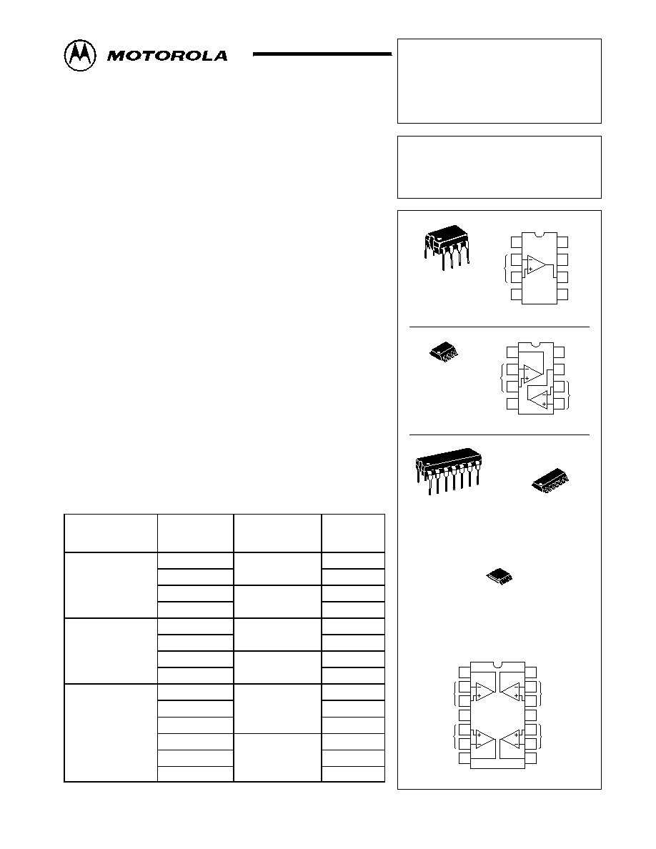
MC33201
MC33202
MC33204
LOW VOLTAGE
RAILTORAIL
OPERATIONAL AMPLIFIERS
Order this document by MC33201/D
P SUFFIX
PLASTIC PACKAGE
CASE 626
(Quad, Top View)
8
1
D SUFFIX
PLASTIC PACKAGE
CASE 751
(SO8)
8
1
P SUFFIX
PLASTIC PACKAGE
CASE 646
14
1
D SUFFIX
PLASTIC PACKAGE
CASE 751A
(SO14)
14
1
Output 1
Inputs 1
VEE
VCC
Output 2
Inputs 2
1
2
6
7
8
5
3
2
1
4
Output 1
Inputs 1
VCC
Output 4
Inputs 4
1
12
13
14
11
3
2
1
4
10
5
9
6
Output 2
8
7
Inputs 2
2
4
3
VEE
Inputs 3
Output 3
(Dual, Top View)
6
7
8
5
3
2
1
4
NC
Inputs
VEE
NC
VCC
NC
Output
(Single, Top View)
DTB SUFFIX
PLASTIC PACKAGE
CASE 948G
(TSSOP14)
14
1
1
MOTOROLA ANALOG IC DEVICE DATA
Rail-to-Rail Operational
Amplifiers
The MC33201/2/4 family of operational amplifiers provide railtorail
operation on both the input and output. The inputs can be driven as high as
200 mV beyond the supply rails without phase reversal on the outputs, and
the output can swing within 50 mV of each rail. This railtorail operation
enables the user to make full use of the supply voltage range available. It is
designed to work at very low supply voltages (
±
0.9 V) yet can operate with a
supply of up to +12 V and ground. Output current boosting techniques
provide a high output current capability while keeping the drain current of the
amplifier to a minimum. Also, the combination of low noise and distortion with
a high slew rate and drive capability make this an ideal amplifier for audio
applications.
·
Low Voltage, Single Supply Operation
(+1.8 V and Ground to +12 V and Ground)
·
Input Voltage Range Includes both Supply Rails
·
Output Voltage Swings within 50 mV of both Rails
·
No Phase Reversal on the Output for Overdriven Input Signals
·
High Output Current (ISC = 80 mA, Typ)
·
Low Supply Current (ID = 0.9 mA, Typ)
·
600
Output Drive Capability
·
Extended Operating Temperature Ranges
(40
°
to +105
°
C and 55
°
to +125
°
C)
·
Typical Gain Bandwidth Product = 2.2 MHz
·
Offered in New TSSOP Package Including Standard SOIC and
DIP Packages
ORDERING INFORMATION
Operational
Amplifier Function
Device
Operating
Temperature
Range
Package
Si
l
MC33201D
TA= 40
°
to +105
°
C
SO8
Single
MC33201P
TA= 40
°
to +105
°
C
Plastic DIP
Single
MC33201VD
TA = 55
°
to
SO8
MC33201VP
A
+125
°
C
Plastic DIP
D
l
MC33202D
TA= 40
°
to +105
°
C
SO8
Dual
MC33202P
TA= 40
°
to +105
°
C
Plastic DIP
Dual
MC33202VD
TA = 55
°
to
SO8
MC33202VP
A
+125
°
C
Plastic DIP
Q
d
MC33204D
T
40
°
105
°
C
SO14
Q
d
MC33204DTB
TA= 40
°
to +105
°
C
TSSOP14
Quad
MC33204P
Plastic DIP
Quad
MC33204VD
TA = 55
°
to
SO14
MC33204VDTB
TA = 55
°
to
+125
°
C
TSSOP14
MC33204VP
+125 C
Plastic DIP
©
Motorola, Inc. 1996
Rev 2
MC33201 MC33202 MC33204
2
MOTOROLA ANALOG IC DEVICE DATA
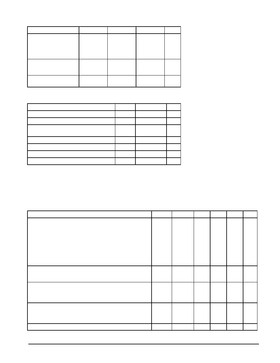
DC ELECTRICAL CHARACTERISTICS
(TA = 25
°
C)
Characteristic
VCC = 2.0 V
VCC = 3.3 V
VCC = 5.0 V
Unit
Input Offset Voltage
VIO (max)
MC33201
MC33202
MC33204
±
8.0
±
10
±
12
±
8.0
±
10
±
12
±
6.0
±
8.0
±
10
mV
Output Voltage Swing
VOH (RL = 10 k
)
VOL (RL = 10 k
)
1.9
0.10
3.15
0.15
4.85
0.15
Vmin
Vmax
Power Supply Current
per Amplifier (ID)
1.125
1.125
1.125
mA
Specifications at VCC = 3.3 V are guaranteed by the 2.0 V and 5.0 V tests. VEE = Gnd.
MAXIMUM RATINGS
Rating
Symbol
Value
Unit
Supply Voltage (VCC to VEE)
VS
+13
V
Input Differential Voltage Range
VIDR
(Note 1)
V
Common Mode Input Voltage Range (Note 2)
VCM
VCC + 0.5 V to
VEE 0.5 V
V
Output Short Circuit Duration
ts
(Note 3)
sec
Maximum Junction Temperature
TJ
+150
°
C
Storage Temperature
Tstg
65 to +150
°
C
Maximum Power Dissipation
PD
(Note 3)
mW
NOTES: 1. The differential input voltage of each amplifier is limited by two internal parallel backtoback
diodes. For additional differential input voltage range, use current limiting resistors in series
with the input pins.
2. The input common mode voltage range is limited by internal diodes connected from the inputs
to both supply rails. Therefore, the voltage on either input must not exceed either supply rail by
more than 500 mV.
3. Power dissipation must be considered to ensure maximum junction temperature (TJ) is not
exceeded. (See Figure 2)
DC ELECTRICAL CHARACTERISTICS
(VCC = + 5.0 V, VEE = Ground, TA = 25
°
C, unless otherwise noted.)
Characteristic
Figure
Symbol
Min
Typ
Max
Unit
Input Offset Voltage (VCM 0 V to 0.5 V, VCM 1.0 V to 5.0 V)
MC33201: TA = + 25
°
C
MC33201:
TA = 40
°
to +105
°
C
MC33201:
TA = 55
°
to +125
°
C
MC33202: TA = + 25
°
C
MC33202:
TA = 40
°
to +105
°
C
MC33202:
TA = 55
°
to +125
°
C
MC33204: TA = + 25
°
C
MC33204:
TA = 40
°
to +105
°
C
MC33204:
TA = 55
°
to +125
°
C
3
VIO
6.0
9.0
13
8.0
11
14
10
13
17
mV
Input Offset Voltage Temperature Coefficient (RS = 50
)
TA = 40
°
to +105
°
C
TA = 55
°
to +125
°
C
4
VIO/
T
2.0
2.0
µ
V/
°
C
Input Bias Current (VCM = 0 V to 0.5 V, VCM = 1.0 V to 5.0 V)
TA = + 25
°
C
TA = 40
°
to +105
°
C
TA = 55
°
to +125
°
C
5, 6
IIB
80
100
200
250
500
nA
Input Offset Current (VCM = 0 V to 0.5 V, VCM = 1.0 V to 5.0 V)
TA = + 25
°
C
TA = 40
°
to +105
°
C
TA = 55
°
to +125
°
C
IIO
5.0
10
50
100
200
nA
Common Mode Input Voltage Range
VICR
VEE
VCC
V
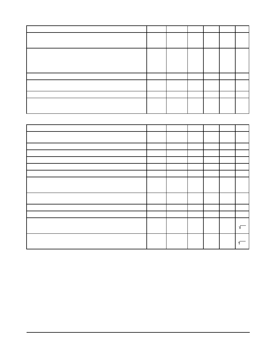
MC33201 MC33202 MC33204
3
MOTOROLA ANALOG IC DEVICE DATA
DC ELECTRICAL CHARACTERISTICS (continued)
(VCC = + 5.0 V, VEE = Ground, TA = 25
°
C, unless otherwise noted.)
Characteristic
Unit
Max
Typ
Min
Symbol
Figure
Large Signal Voltage Gain (VCC = + 5.0 V, VEE = 5.0 V)
RL = 10 k
RL = 600
7
AVOL
50
25
300
250
kV/V
Output Voltage Swing (VID =
±
0.2 V)
RL = 10 k
RL = 10 k
RL = 600
RL = 600
8, 9, 10
VOH
VOL
VOH
VOL
4.85
4.75
4.95
0.05
4.85
0.15
0.15
0.25
V
Common Mode Rejection (Vin = 0 V to 5.0 V)
11
CMR
60
90
dB
Power Supply Rejection Ratio
VCC/VEE = 5.0 V/Gnd to 3.0 V/Gnd
12
PSRR
500
25
µ
V/V
Output Short Circuit Current (Source and Sink)
13, 14
ISC
50
80
mA
Power Supply Current per Amplifier (VO = 0 V)
TA = 40
°
to +105
°
C
TA = 55
°
to +125
°
C
15
ID
0.9
0.9
1.125
1.125
mA
AC ELECTRICAL CHARACTERISTICS
(VCC = + 5.0 V, VEE = Ground, TA = 25
°
C, unless otherwise noted.)
Characteristic
Figure
Symbol
Min
Typ
Max
Unit
Slew Rate
(VS =
±
2.5 V, VO = 2.0 V to + 2.0 V, RL = 2.0 k
, AV = +1.0)
16, 26
SR
0.5
1.0
V/
µ
s
Gain Bandwidth Product (f = 100 kHz)
17
GBW
2.2
MHz
Gain Margin (RL = 600
, CL = 0 pF)
20, 21, 22
AM
12
dB
Phase Margin (RL = 600
, CL = 0 pF)
20, 21, 22
O
M
65
Deg
Channel Separation (f = 1.0 Hz to 20 kHz, AV = 100)
23
CS
90
dB
Power Bandwidth (VO = 4.0 Vpp, RL = 600
, THD
1 %)
BWP
28
kHz
Total Harmonic Distortion (RL = 600
, VO = 1.0 Vpp, AV = 1.0)
f = 1.0 kHz
f = 10 kHz
24
THD
0.002
0.008
%
Open Loop Output Impedance
(VO = 0 V, f = 2.0 MHz, AV = 10)
ZO
100
Differential Input Resistance (VCM = 0 V)
Rin
200
k
Differential Input Capacitance (VCM = 0 V)
Cin
8.0
pF
Equivalent Input Noise Voltage (RS = 100
)
f = 10 Hz
f = 1.0 kHz
25
en
25
20
Hz
nV/
Equivalent Input Noise Current
f = 10 Hz
f = 1.0 kHz
25
in
0.8
0.2
pA/
Hz
MC33201 MC33202 MC33204
4
MOTOROLA ANALOG IC DEVICE DATA
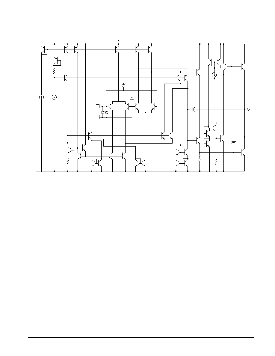
Vin
Vout
Figure 1. Circuit Schematic
(Each Amplifier)
VEE
VCC
VCC
VCC
VCC
Vin +
VEE
This device contains 70 active transistors (each amplifier).
MC33201 MC33202 MC33204
5
MOTOROLA ANALOG IC DEVICE DATA
300
260
220
180
TA, AMBIENT TEMPERATURE (
°
C)
100
140
PERCENT
AGE OF
AMPLIFIERS
(%)
TCVIO, INPUT OFFSET VOLTAGE TEMPERATURE COEFFICIENT (
µ
V/
°
C)
50
30
0
40
10
20
A
VOL
, OPEN LOOP
VOL
T
AGE GAIN (kV/V)
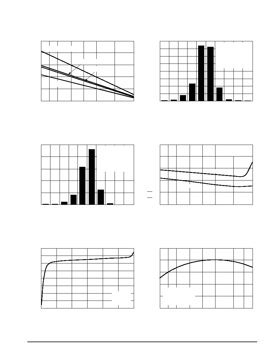
Figure 2. Maximum Power Dissipation
versus Temperature
Figure 3. Input Offset Voltage Distribution
PERCENT
AGE OF
AMPLIFIERS
(%)
40
35
VIO, INPUT OFFSET VOLTAGE (mV)
30
25
15
0
20
Figure 4. Input Offset Voltage
Temperature Coefficient Distribution
2500
2000
1000
500
0
TA, AMBIENT TEMPERATURE (
°
C)
Figure 5. Input Bias Current
versus Temperature
Figure 6. Input Bias Current
versus Common Mode Voltage
Figure 7. Open Loop Voltage Gain versus
Temperature
150
50
0
50
VCM, INPUT COMMON MODE VOLTAGE (V)
1500
P
D(max)
, MAXIMUM POWER DISSIP
A
TION (mW)
200
160
120
80
TA, AMBIENT TEMPERATURE (
°
C)
0
I IB
, INPUT
BIAS CURRENT
(nA)
40
5.0
10
VCC = + 5.0 V
VEE = Gnd
VCM > 1.0 V
VCM = 0 V to 0.5 V
I IB
, INPUT
BIAS CURRENT
(nA)
100
100
150
200
250
55 40 25
0
25
70
85
125
50
0
20
40
50
10
10
30
30
40
20
10
0
4.0
8.0
10
55 40 25
0
25
50
85
125
2.0
4.0
2.0
2.0
6.0
6.0
8.0
4.0
55 40 25
0
25
70
85
125
0
6.0
8.0
10
12
105
8 and 14 Pin DIP Pkg
SO14 Pkg
SO8 Pkg
360 amplifiers tested from
3 (MC33204) wafer lots
VCC = + 5.0 V
VEE = Gnd
TA = 25
°
C
DIP Package
360 amplifiers tested from
3 (MC33204) wafer lots
VCC = + 5.0 V
VEE = Gnd
TA = 25
°
C
DIP Package
VCC = + 5.0 V
VEE = Gnd
RL = 600
VO = 0.5 V to 4.5 V
VCC = 12 V
VEE = Gnd
TA = 25
°
C
TSSOP14 Pkg
MC33201 MC33202 MC33204
6
MOTOROLA ANALOG IC DEVICE DATA
V
O
,
OUTPUT
VOL
T
AGE (V
)
pp
V
O
,
OUTPUT
VOL
T
AGE (V
)
pp
40
20
100
80
60
Vout
, OUTPUT VOLTAGE (V)
0
f, FREQUENCY (Hz)
12
0
9.0
3.0
6.0
VCC = + 6.0 V
VEE = 6.0 V
RL = 600
AV = +1.0
TA = 25
°
C
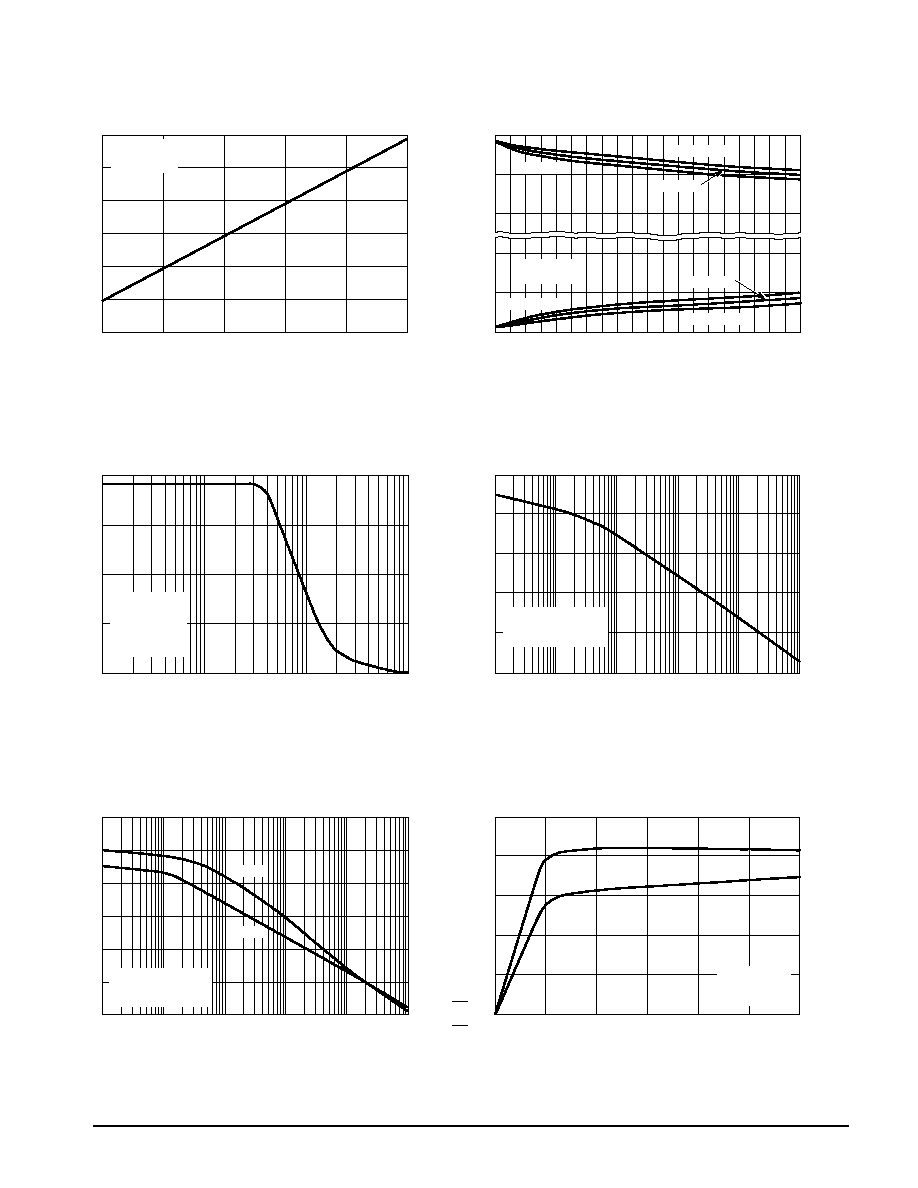
Figure 8. Output Voltage Swing
versus Supply Voltage
Figure 9. Output Saturation Voltage
versus Load Current
V
IL, LOAD CURRENT (mA)
VEE
Figure 10. Output Voltage
versus Frequency
12
10
6.0
2.0
0
VCC,
VEE
SUPPLY VOLTAGE (V)
Figure 11. Common Mode Rejection
versus Frequency
Figure 12. Power Supply Rejection
versus Frequency
Figure 13. Output Short Circuit Current
versus Output Voltage
120
80
60
f, FREQUENCY (Hz)
8.0
100
80
60
40
f, FREQUENCY (Hz)
0
CMR, COMMON MODE REJECTION (dB)
20
VCC = + 6.0 V
VEE = 6.0 V
TA = 55
°
to +125
°
C
PSR, POWER SUPPL
Y
REJECTION (dB)
100
40
20
0
VCC = + 6.0 V
VEE = 6.0 V
TA = 55
°
to +125
°
C
VCC = + 6.0 V
VEE = 6.0 V
TA = 25
°
C
4.0
SA
T
, OUTPUT
SA
TURA
TION VOL
T
AGE
(V)
TA = 25
°
C
TA = 55
°
C
PSR+
PSR
I SC
, OUTPUT
SHOR
T
CIRCUIT
CURRENT
(mA)
Source
Sink
VCC = + 5.0 V
VEE = 5.0 V
TA = 125
°
C
TA = 125
°
C
TA = 55
°
C
TA = 25
°
C
10
100
1.0 k
10 k
100 k
1.0 M
0
1.0
2.0
3.0
4.0
5.0
6.0
1.0 k
100 k
1.0 M
10 k
0
15
20
±
1.0
±
2.0
10
5.0
10
100
1.0 k
10 k
100 k
1.0 M
±
3.0
±
4.0
±
5.0
±
6.0
RL = 600
TA = 25
°
C
VCC
VCC 0.2 V
VCC 0.4 V
VEE + 0.4 V
VEE + 0.2 V
MC33201 MC33202 MC33204
7
MOTOROLA ANALOG IC DEVICE DATA
, EXCESS PHASE (DEGREES)
VCC,
VEE
, SUPPLY VOLTAGE (V)
I SC
, OUTPUT
SHOR
T
CIRCUIT
CURRENT
(mA)
SR,
SLEW
RA
TE (V/ s)
µ
TA, AMBIENT TEMPERATURE (
°
C)
VCC = + 2.5 V
VEE = 2.5 V
VO =
±
2.0 V
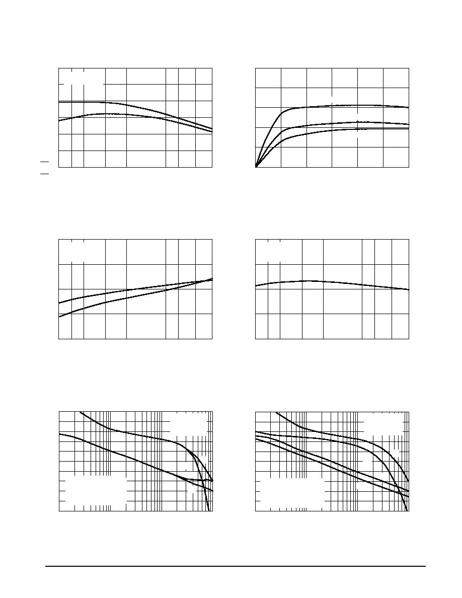
Figure 14. Output Short Circuit Current
versus Temperature
Figure 15. Supply Current per Amplifier
versus Supply Voltage with No Load
I
Figure 16. Slew Rate
versus Temperature
TA, AMBIENT TEMPERATURE (
°
C)
Figure 17. Gain Bandwidth Product
versus Temperature
Figure 18. Voltage Gain and Phase
versus Frequency
Figure 19. Voltage Gain and Phase
versus Frequency
f, FREQUENCY (Hz)
GBW
, GAIN BANDWIDTH PRODUCT
(MHz)
A
, OPEN LOOP
VOL
T
AGE
GAIN
(dB)
VCC = + 5.0 V
VEE = Gnd
CC
, SUPPL
Y
CURRENT
PER
AMPLIFIER
(mA)
TA = 125
°
C
TA = 55
°
C
Source
Sink
TA = 25
°
C
+Slew Rate
Slew Rate
TA, AMBIENT TEMPERATURE (
°
C)
VCC = + 2.5 V
VEE = 2.5 V
f = 100 kHz
VOL
, EXCESS PHASE (DEGREES)
f, FREQUENCY (Hz)
O
O
70
50
30
10
10
30
2.0
0
1.5
0.5
1.0
2.0
1.6
0
150
125
75
25
0
70
50
30
100
4.0
3.0
2.0
0
1.0
10
10
30
50
1.2
0.8
0.4
±
1.0
±
2.0
±
3.0
±
4.0
±
5.0
±
6.0
10 k
100 k
1.0 M
10 M
55 40 25
25
70
125
0
85
105
±
0
55 40 25
25
70
125
0
85
105
55 40 25
25
70
125
0
85
105
10 k
100 k
1.0 M
10 M
240
40
80
120
160
200
40
80
120
160
200
240
A
, OPEN LOOP
VOL
T
AGE
GAIN
(dB)
VOL
1A Phase, CL = 0 pF
1B Gain, CL = 0 pF
2A Phase, CL = 300 pF
2B Gain, CL = 300 pF
1A Phase, VS =
±
6.0 V
1B Gain, VS =
±
6.0 V
2A Phase, VS =
±
1.0 V
2B Gain, VS =
±
1.0 V
VS =
±
6.0 V
TA = 25
°
C
RL = 600
CL = 0 pF
TA = 25
°
C
RL = 600
1
A
2
A2
B
1
B
1
A
2
A
2
B
1
B
MC33201 MC33202 MC33204
8
MOTOROLA ANALOG IC DEVICE DATA
M
, PHASE MARGIN (DEGREES)
i , INPUT
REFERRED
NOISE
CURRENT
(pA/ Hz)
n
50
40
30
e , EQUIV
ALENT
INPUT
NOISE VOL
T
AGE (nV/ Hz)
20
10
0
n
RT, DIFFERENTIAL SOURCE RESISTANCE (
)
CL, CAPACITIVE LOAD (pF)
80
0
70
40
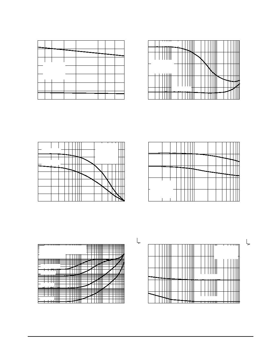
Figure 20. Gain and Phase Margin
versus Temperature
Figure 21. Gain and Phase Margin
versus Differential Source Resistance
75
60
0
Figure 22. Gain and Phase Margin
versus Capacitive Load
70
60
40
10
0
TA, AMBIENT TEMPERATURE (
°
C)
Figure 23. Channel Separation
versus Frequency
Figure 24. Total Harmonic Distortion
versus Frequency
Figure 25. Equivalent Input Noise Voltage
and Current versus Frequency
10
1.0
0.1
f, FREQUENCY (Hz)
50
150
90
60
0
CS, CHANNEL
SEP
ARA
TION
(dB)
30
THD,
T
O
T
A
L
HARMONIC DIST
OR
TION (%)
0.01
0.001
20
45
30
15
Phase Margin
Gain Margin
f, FREQUENCY (Hz)
f, FREQUENCY (Hz)
M
, PHASE MARGIN (DEGREES)
30
A
M
, GAIN MARGIN (dB)
A
M
, GAIN MARGIN (dB)
60
10
20
30
50
A
M
, GAIN MARGIN (dB)
AV = 10
120
AV = 100
AV = 10
AV = 1.0
AV = 100
M
, PHASE MARGIN (DEGREES)
O
O
O
100
1.0 k
10 k
100 k
10
100
1.0 k
100 k
55 40 25
25
70
125
0
85
105
10
10
100
1.0 k
100
1.0 k
10 k
10
100
10 k
100 k
10 k
1.0 k
5.0
4.0
3.0
2.0
1.0
0
70
60
40
10
0
50
20
30
75
60
0
45
30
15
16
0
14
8.0
12
2.0
4.0
6.0
10
VCC = + 6.0 V
VEE = 6.0 V
RL = 600
CL = 100 pF
VCC = + 6.0 V
VEE = 6.0 V
TA = 25
°
C
Phase Margin
Phase Margin
Gain Margin
VCC = + 6.0 V
VEE = 6.0 V
RL = 600
AV = 100
TA = 25
°
C
Gain Margin
VCC = + 6.0 V
VEE = 6.0 V
VO = 8.0 Vpp
TA = 25
°
C
VCC = + 5.0 V
TA = 25
°
C
VO = 2.0 Vpp
VEE = 5.0 V
RL = 600
VCC = + 6.0 V
VEE = 6.0 V
TA = 25
°
C
Noise Voltage
Noise Current
AV = 1000
MC33201 MC33202 MC33204
9
MOTOROLA ANALOG IC DEVICE DATA
General Information
The MC33201/2/4 family of operational amplifiers are
unique in their ability to swing railtorail on both the input
and the output with a completely bipolar design. This offers
low noise, high output current capability and a wide common
mode input voltage range even with low supply voltages.
Operation is guaranteed over an extended temperature
range and at supply voltages of 2.0 V, 3.3 V and 5.0 V and
ground.
Since the common mode input voltage range extends from
VCC to VEE, it can be operated with either single or split
voltage supplies. The MC33201/2/4 are guaranteed not to
latch or phase reverse over the entire common mode range,
however, the inputs should not be allowed to exceed
maximum ratings.
Circuit Information
Railtorail performance is achieved at the input of the
amplifiers by using parallel NPNPNP differential input
stages. When the inputs are within 800 mV of the negative
rail, the PNP stage is on. When the inputs are more than 800
mV greater than VEE, the NPN stage is on. This switching of
input pairs will cause a reversal of input bias currents (see
Figure 6). Also, slight differences in offset voltage may be
noted between the NPN and PNP pairs. Crosscoupling
techniques have been used to keep this change to a
minimum.
In addition to its railtorail performance, the output stage
is current boosted to provide 80 mA of output current,
enabling the op amp to drive 600
loads. Because of this
high output current capability, care should be taken not to
exceed the 150
°
C maximum junction temperature.
O
,
OUTPUT
VOL
T
AGE (50 mV/DIV)
V
t, TIME (10
µ
s/DIV)
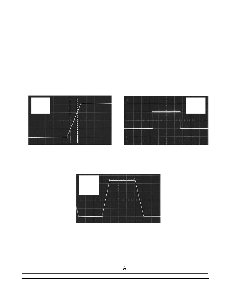
Figure 26. Noninverting Amplifier Slew Rate
Figure 27. Small Signal Transient Response
t, TIME (5.0
µ
s/DIV)
Figure 28. Large Signal Transient Response
VCC = + 6.0 V
VEE = 6.0 V
RL = 600
CL = 100 pF
TA = 25
°
C
O
,
OUTPUT
VOL
T
AGE (2.0 mV/DIV)
VCC = + 6.0 V
VEE = 6.0 V
RL = 600
CL = 100 pF
AV = 1.0
TA = 25
°
C
V
VCC = + 6.0 V
VEE = 6.0 V
RL = 600
CL = 100 pF
TA = 25
°
C
t, TIME (10
µ
s/DIV)
O
,
OUTPUT
VOL
T
AGE (2.0 V/DIV)
V
Motorola reserves the right to make changes without further notice to any products herein. Motorola makes no warranty, representation or guarantee regarding
the suitability of its products for any particular purpose, nor does Motorola assume any liability arising out of the application or use of any product or circuit, and
specifically disclaims any and all liability, including without limitation consequential or incidental damages. "Typical" parameters which may be provided in Motorola
data sheets and/or specifications can and do vary in different applications and actual performance may vary over time. All operating parameters, including "Typicals"
must be validated for each customer application by customer's technical experts. Motorola does not convey any license under its patent rights nor the rights of
others. Motorola products are not designed, intended, or authorized for use as components in systems intended for surgical implant into the body, or other
applications intended to support or sustain life, or for any other application in which the failure of the Motorola product could create a situation where personal injury
or death may occur. Should Buyer purchase or use Motorola products for any such unintended or unauthorized application, Buyer shall indemnify and hold Motorola
and its officers, employees, subsidiaries, affiliates, and distributors harmless against all claims, costs, damages, and expenses, and reasonable attorney fees
arising out of, directly or indirectly, any claim of personal injury or death associated with such unintended or unauthorized use, even if such claim alleges that
Motorola was negligent regarding the design or manufacture of the part. Motorola and are registered trademarks of Motorola, Inc. Motorola, Inc. is an Equal
Opportunity/Affirmative Action Employer.
MC33201 MC33202 MC33204
10
MOTOROLA ANALOG IC DEVICE DATA
OUTLINE DIMENSIONS
P SUFFIX
PLASTIC PACKAGE
CASE 62605
ISSUE K
D SUFFIX
PLASTIC PACKAGE
CASE 75105
(SO8)
ISSUE R
NOTES:
1. DIMENSION L TO CENTER OF LEAD WHEN
FORMED PARALLEL.
2. PACKAGE CONTOUR OPTIONAL (ROUND OR
SQUARE CORNERS).
3. DIMENSIONING AND TOLERANCING PER ANSI
Y14.5M, 1982.
1
4
5
8
F
NOTE 2
A
B
T
SEATING
PLANE
H
J
G
D
K
N
C
L
M
M
A
M
0.13 (0.005)
B
M
T
DIM
MIN
MAX
MIN
MAX
INCHES
MILLIMETERS
A
9.40
10.16
0.370
0.400
B
6.10
6.60
0.240
0.260
C
3.94
4.45
0.155
0.175
D
0.38
0.51
0.015
0.020
F
1.02
1.78
0.040
0.070
G
2.54 BSC
0.100 BSC
H
0.76
1.27
0.030
0.050
J
0.20
0.30
0.008
0.012
K
2.92
3.43
0.115
0.135
L
7.62 BSC
0.300 BSC
M
10
10
N
0.76
1.01
0.030
0.040
_
_
SEATING
PLANE
1
4
5
8
A
0.25
M
C B
S
S
0.25
M
B
M
h
q
C
X 45
_
L
DIM
MIN
MAX
MILLIMETERS
A
1.35
1.75
A1
0.10
0.25
B
0.35
0.49
C
0.18
0.25
D
4.80
5.00
E
1.27 BSC
e
3.80
4.00
H
5.80
6.20
h
0
7
L
0.40
1.25
q
0.25
0.50
_
_
NOTES:
1. DIMENSIONING AND TOLERANCING PER ASME
Y14.5M, 1994.
2. DIMENSIONS ARE IN MILLIMETERS.
3. DIMENSION D AND E DO NOT INCLUDE MOLD
PROTRUSION.
4. MAXIMUM MOLD PROTRUSION 0.15 PER SIDE.
5. DIMENSION B DOES NOT INCLUDE MOLD
PROTRUSION. ALLOWABLE DAMBAR
PROTRUSION SHALL BE 0.127 TOTAL IN EXCESS
OF THE B DIMENSION AT MAXIMUM MATERIAL
CONDITION.
D
E
H
A
B
e
B
A1
C
A
0.10
P SUFFIX
PLASTIC PACKAGE
CASE 64606
ISSUE L
NOTES:
1. LEADS WITHIN 0.13 (0.005) RADIUS OF TRUE
POSITION AT SEATING PLANE AT MAXIMUM
MATERIAL CONDITION.
2. DIMENSION L TO CENTER OF LEADS WHEN
FORMED PARALLEL.
3. DIMENSION B DOES NOT INCLUDE MOLD
FLASH.
4. ROUNDED CORNERS OPTIONAL.
1
7
14
8
B
A
F
H
G
D
K
C
N
L
J
M
SEATING
PLANE
DIM
MIN
MAX
MIN
MAX
MILLIMETERS
INCHES
A
0.715
0.770
18.16
19.56
B
0.240
0.260
6.10
6.60
C
0.145
0.185
3.69
4.69
D
0.015
0.021
0.38
0.53
F
0.040
0.070
1.02
1.78
G
0.100 BSC
2.54 BSC
H
0.052
0.095
1.32
2.41
J
0.008
0.015
0.20
0.38
K
0.115
0.135
2.92
3.43
L
0.300 BSC
7.62 BSC
M
0
10 0 10
N
0.015
0.039
0.39
1.01
_
_
_
_
MC33201 MC33202 MC33204
11
MOTOROLA ANALOG IC DEVICE DATA
OUTLINE DIMENSIONS
D SUFFIX
PLASTIC PACKAGE
CASE 751A03
(SO14)
ISSUE F
NOTES:
1. DIMENSIONING AND TOLERANCING PER ANSI
Y14.5M, 1982.
2. CONTROLLING DIMENSION: MILLIMETER.
3. DIMENSIONS A AND B DO NOT INCLUDE
MOLD PROTRUSION.
4. MAXIMUM MOLD PROTRUSION 0.15 (0.006)
PER SIDE.
5. DIMENSION D DOES NOT INCLUDE DAMBAR
PROTRUSION. ALLOWABLE DAMBAR
PROTRUSION SHALL BE 0.127 (0.005) TOTAL
IN EXCESS OF THE D DIMENSION AT
MAXIMUM MATERIAL CONDITION.
A
B
G
P
7 PL
14
8
7
1
M
0.25 (0.010)
B
M
S
B
M
0.25 (0.010)
A
S
T
T
F
R
X 45
SEATING
PLANE
D
14 PL
K
C
J
M
_
DIM
MIN
MAX
MIN
MAX
INCHES
MILLIMETERS
A
8.55
8.75
0.337
0.344
B
3.80
4.00
0.150
0.157
C
1.35
1.75
0.054
0.068
D
0.35
0.49
0.014
0.019
F
0.40
1.25
0.016
0.049
G
1.27 BSC
0.050 BSC
J
0.19
0.25
0.008
0.009
K
0.10
0.25
0.004
0.009
M
0
7
0
7
P
5.80
6.20
0.228
0.244
R
0.25
0.50
0.010
0.019
_
_
_
_
DTB SUFFIX
PLASTIC PACKAGE
CASE 948G01
(TSSOP14)
ISSUE O
DIM
MIN
MAX
MIN
MAX
INCHES
MILLIMETERS
A
4.90
5.10
0.193
0.200
B
4.30
4.50
0.169
0.177
C
1.20
0.047
D
0.05
0.15
0.002
0.006
F
0.50
0.75
0.020
0.030
G
0.65 BSC
0.026 BSC
H
0.50
0.60
0.020
0.024
J
0.09
0.20
0.004
0.008
J1
0.09
0.16
0.004
0.006
K
0.19
0.30
0.007
0.012
K1
0.19
0.25
0.007
0.010
L
6.40 BSC
0.252 BSC
M
0
8
0
8
NOTES:
1 DIMENSIONING AND TOLERANCING PER ANSI
Y14.5M, 1982.
2 CONTROLLING DIMENSION: MILLIMETER.
3 DIMENSION A DOES NOT INCLUDE MOLD FLASH,
PROTRUSIONS OR GATE BURRS. MOLD FLASH
OR GATE BURRS SHALL NOT EXCEED 0.15
(0.006) PER SIDE.
4 DIMENSION B DOES NOT INCLUDE INTERLEAD
FLASH OR PROTRUSION. INTERLEAD FLASH OR
PROTRUSION SHALL NOT EXCEED
0.25 (0.010) PER SIDE.
5 DIMENSION K DOES NOT INCLUDE DAMBAR
PROTRUSION. ALLOWABLE DAMBAR
PROTRUSION SHALL BE 0.08 (0.003) TOTAL IN
EXCESS OF THE K DIMENSION AT MAXIMUM
MATERIAL CONDITION.
6 TERMINAL NUMBERS ARE SHOWN FOR
REFERENCE ONLY.
7 DIMENSION A AND B ARE TO BE DETERMINED
AT DATUM PLANE W.
_
_
_
_
S
U
0.15 (0.006) T
2X
L/2
S
U
M
0.10 (0.004)
V
S
T
L
U
SEATING
PLANE
0.10 (0.004)
T
ÇÇÇ
ÇÇÇ
ÇÇÇ
SECTION NN
DETAIL E
J J1
K
K1
ÉÉÉ
ÉÉÉ
DETAIL E
F
M
W
0.25 (0.010)
8
14
7
1
PIN 1
IDENT.
H
G
A
D
C
B
S
U
0.15 (0.006) T
V
14X REF
K
N
N
How to reach us:
USA / EUROPE / Locations Not Listed: Motorola Literature Distribution;
JAPAN: Nippon Motorola Ltd.; TatsumiSPDJLDC, 6F SeibuButsuryuCenter,
P.O. Box 20912; Phoenix, Arizona 85036. 18004412447 or 6023035454
3142 Tatsumi KotoKu, Tokyo 135, Japan. 038135218315
MFAX: RMFAX0@email.sps.mot.com TOUCHTONE 6022446609
ASIA/PACIFIC: Motorola Semiconductors H.K. Ltd.; 8B Tai Ping Industrial Park,
INTERNET: http://DesignNET.com
51 Ting Kok Road, Tai Po, N.T., Hong Kong. 85226629298
MC33201/D
*MC33201/D*