 | ÐлекÑÑоннÑй компоненÑ: MC3357D | СкаÑаÑÑ:  PDF PDF  ZIP ZIP |
Äîêóìåíòàöèÿ è îïèñàíèÿ www.docs.chipfind.ru
Device
Operating
Temperature Range
Package
MC3357
SEMICONDUCTOR
TECHNICAL DATA
LOW POWER
FM IF
ORDERING INFORMATION
MC3357D
MC3357P
TA = 30 to +70
°
C
SO16
Plastic DIP
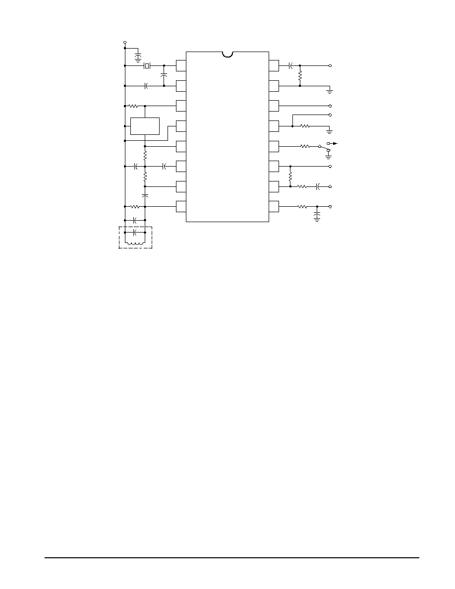
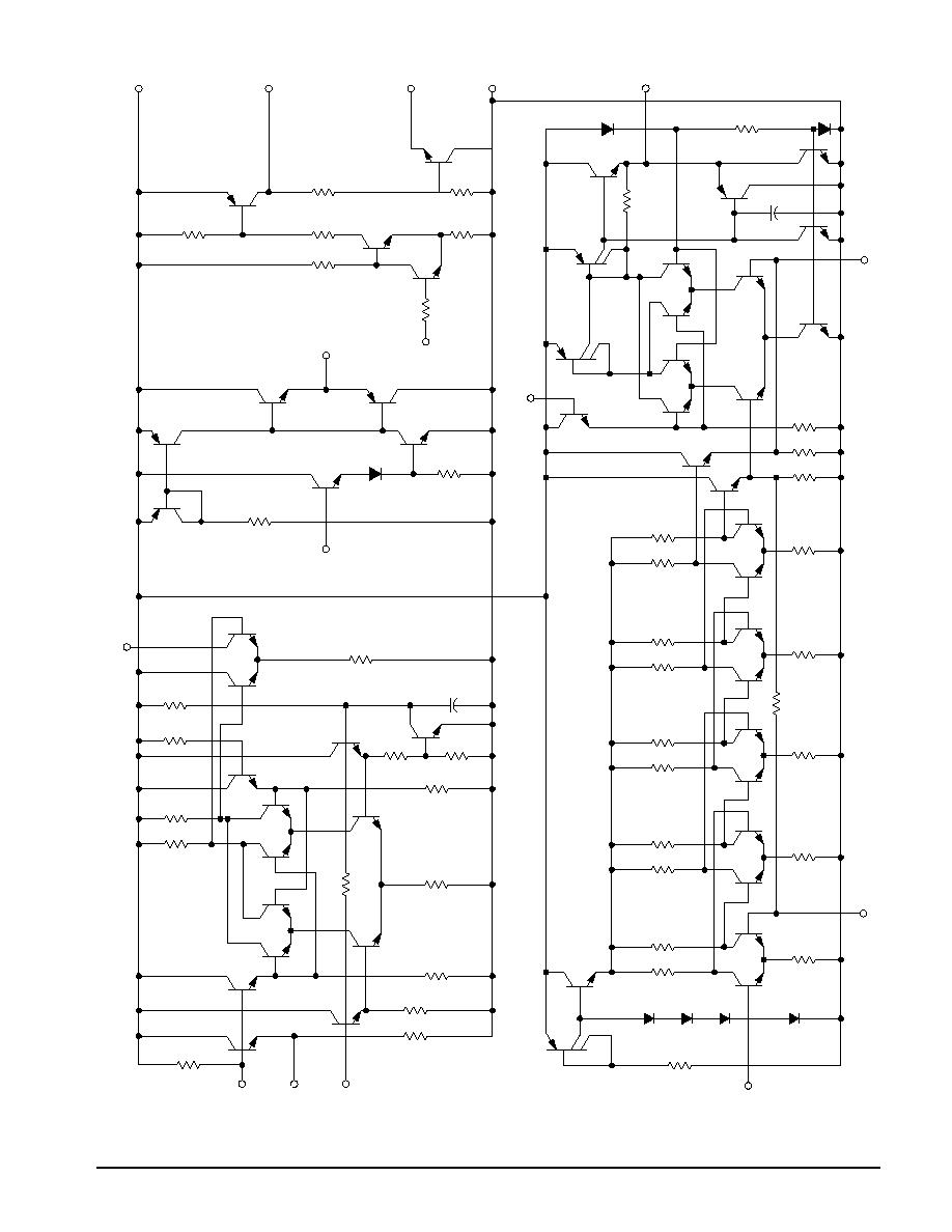
PIN CONNECTIONS
Order this document by MC3357/D
P SUFFIX
PLASTIC PACKAGE
CASE 648
D SUFFIX
PLASTIC PACKAGE
CASE 751B
(SO16)
2
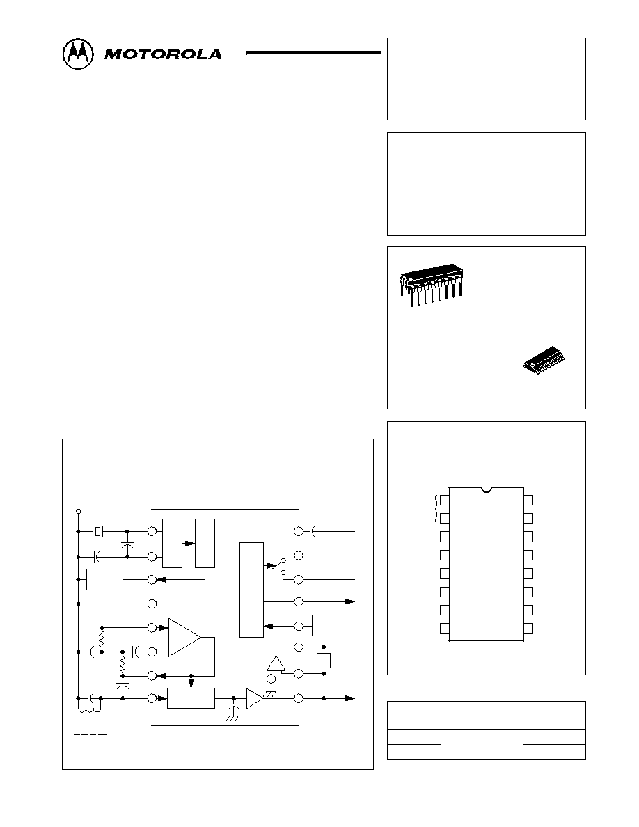
3
Crystal
Osc.
VCC
Limiter
Input
Decoupling
Limiter
Output
Quad
Input
RF
Input
9
10
11
12
13
14
15
16
1
4
5
6
7
8
Gnd
Audio
Mute
Scan
Control
Squelch
Input
Filter
Output
Filter
Input
Demodulator
Output
Mixer
Output
1
MOTOROLA ANALOG IC DEVICE DATA
Low Power Narrowband FM IF
. . . includes Oscillator, Mixer, Limiting Amplifier, Quadrature Discriminator,
Active Filter, Squelch, Scan Control, and Mute Switch. The MC3357 is
designed for use in FM dual conversion communications equipment.
·
Low Drain Current (3.0 mA (Typical) @ VCC = 6.0 Vdc)
·
Excellent Sensitivity: Input Limiting Voltage
( 3.0 dB) = 5.0
µ
V (Typical)
·
Low Number of External Parts Required
·
Recommend MC3372 for Replacement/Upgrade
Figure 1. Representative Block Diagram
10.7 MHz Input
Ground
Z2
Audio
Noise
Detector
Z1
Audio Mute
Scan Control
Active
Filter
Amp
_
2.0 V
+
455 kHz
Filter
10.245 MHz
VCC
Quad
Coil
Demodulator
Limiter
Amp
16
14
15
13
12
11
10
9
8
7
6
5
4
3
2
1
Oscillator
Mixer
Squelch T
rigger
With Hysteresis
©
Motorola, Inc. 1996
Rev 5
MC3357
2
MOTOROLA ANALOG IC DEVICE DATA
MAXIMUM RATINGS
(TA = 25
°
C, unless otherwise noted)
Rating
Pin
Symbol
Value
Unit
Power Supply Voltage
4
VCC(max)
12
Vdc
Operating Supply Voltage Range
4
VCC
4 to 8
Vdc
Detector Input Voltage
8
1.0
Vpp
Input Voltage (VCC
q
6.0 Volts)
16
V16
1.0
VRMS
Mute Function
14
V14
0.5 to 5.0
Vpk
Junction Temperature
TJ
150
°
C
Operating Ambient Temperature Range
TA
30 to + 70
°
C
Storage Temperature Range
Tstg
65 to + 150
°
C
ELECTRICAL CHARACTERISTICS
(VCC = 6.0 Vdc, fo = 10.7 MHz,
f =
±
3.0 kHz, fmod = 1.0 kHz, TA = 25
°
C, unless otherwise noted.)
Characteristic
Pin
Min
Typ
Max
Unit
Drain Current
Squelch Off
Drain Current
Squelch On
4
2.0
3.0
5.0
mA
Input Limiting Voltage ( 3 dB Limiting)
16
5.0
10
µ
V
Detector Output Voltage
9
3.0
Vdc
Detector Output Impedance
400
Recovered Audio Output Voltage (Vin = 10 mV)
9
200
350
mVrms
Filter Gain (10 kHz) (Vin = 5 mV)
40
46
dB
Filter Output Voltage
11
1.8
2.0
2.5
Vdc
Trigger Hysteresis
100
mV
Mute Function Low
14
15
50
Mute Function High
14
1.0
10
M
Scan Function Low (Mute Off)
(V12 = 2 Vdc)
13
0
0.5
Vdc
Scan Function High (Mute On)
(V12 = Gnd)
13
5.0
Vdc
Mixer Conversion Gain
3
20
dB
Mixer Input Resistance
16
3.3
k
Mixer Input Capacitance
16
2.2
pF
MC3357
3
MOTOROLA ANALOG IC DEVICE DATA
Figure 2. Test Circuit
20 pF
120 pF
0.1
µ
F
VCC = 6.0 Vdc
10.245 MHz
50 pF
2.0 k
455 kHz
Filter
100 nF
2.0 k
51 k
100 nF
47 k
10 pF
LP = 1.0 mH
CP = 100 pF
RP = 100 k
muRata
CFU
455 D
8.2 k
390 k
1.0 k
1.0
µ
F
Filter In
Audio Out
100 nF
10 k
10 k
51
Input
10.7 MHz
9
10
11
12
13
14
15
16
4
3
2
1
0.01
µ
F
2.0 Vdc
Op Amp Output
5
6
7
8
+
CIRCUIT DESCRIPTION
The MC3357 is a low power FM IF circuit designed
primarily for use in voice communication scanning receivers.
The mixeroscillator combination converts the input
frequency (e.g., 10.7 MHz) down to 455 kHz, where, after
external bandpass filtering, most of the amplification is done.
The audio is recovered using a conventional quadrature FM
detector. The absence of an input signal is indicated by the
presence of noise above the desired audio frequencies. This
"noise band" is monitored by an active filter and a detector. A
squelch trigger circuit indicates the presence of a noise (or a
tone) by an output which can be used to control scanning. At
the same time, an internal switch is operated which can be
used to mute the audio.
The oscillator is an internallybiased Colpitts type with the
collector, base, and emitter connections at Pins 4, 1, and 2
respectively. A crystal can be used in place of the usual coil.
The mixer is doublybalanced to reduce spurious
responses. The input impedance at Pin 16 is set by a 3.0 k
internal biasing resistor and has low capacitance, allowing
the circuit to be preceded by a crystal filter. The collector
output at Pin 3 must be dc connected to B +, below which it
can swing 0.5 V.
After suitable bandpass filtering (ceramic or LC), the signal
goes to the input of a fivestage limiter at Pin 5. The output of
the limiter at Pin 7 drives a multiplier, both internally directly,
and externally through a quadrature coil, to detect the FM. The
output at Pin 7 is also used to supply dc feedback to Pin 5. The
other side of the first limiter stage is decoupled at Pin 6.
The recovered audio is partially filtered, then buffered,
giving an impedance of around 400
at Pin 9. The signal still
requires deemphasis, volume control and further
amplification before driving a loudspeaker.
A simple inverting op amp is provided with an output at Pin
11 providing dc bias (externally) to the input at Pin 10 which is
referred internally to 2.0 V. A filter can be made with external
impedance elements to discriminate between frequencies.
With an external AM detector, the filtered audio signal can be
checked for the presence of noise above the normal audio
band, or a tone signal. This information is applied to Pin 12.
An external positive bias to Pin 12 sets up the squelch
trigger circuit such that Pin 13 is low at an impedance level of
around 60 k
, and the audio mute (Pin 14) is open circuit. If
Pin 12 is pulled down to 0.7 V by the noise or tone detector,
Pin 13 will rise to approximately 0.5 Vdc below supply where
it can support a load current of around 500
µ
A and Pin 14 is
internally shortcircuited to ground. There is 100 mV of
hysteresis at Pin 12 to prevent jitter. Audio muting is
accomplished by connecting Pin 14 to a highimpedance
groundreference point in the audio path between Pin 9 and
the audio amplifier.
MC3357
4
MOTOROLA ANALOG IC DEVICE DATA
4
13
14
15
9
3.0 k
2
16
5
15 k
100 k
100 k
30 k
30 k
8
9
34
5.0 k
30 k
15 k
15 k
11
10
5
10 k
10 k
30 k
20 k
3
14
15
20 k
10
50 k
22
21
20
19
18
16
17
50 k
12
11
22 k
23
24
25
26
220 k
15 k
10 k
50 k
470
50 k
C 1
27
32
28
29
30
31
10 k
10 k
10 k
10 k
10 k
10 k
10 k
10 k
10 k
10 k
33
34
35
36
37
38
39
40
41
42
6.2 k
33 k
33 k
33 k
33 k
10 k
120 k
10
k
44
43
45
52
49
48
46
50
51
53
54
55
58
57
56
50 k
100 k
C 2
8
Figure 3. Circuit Schematic
MC3357
5
MOTOROLA ANALOG IC DEVICE DATA
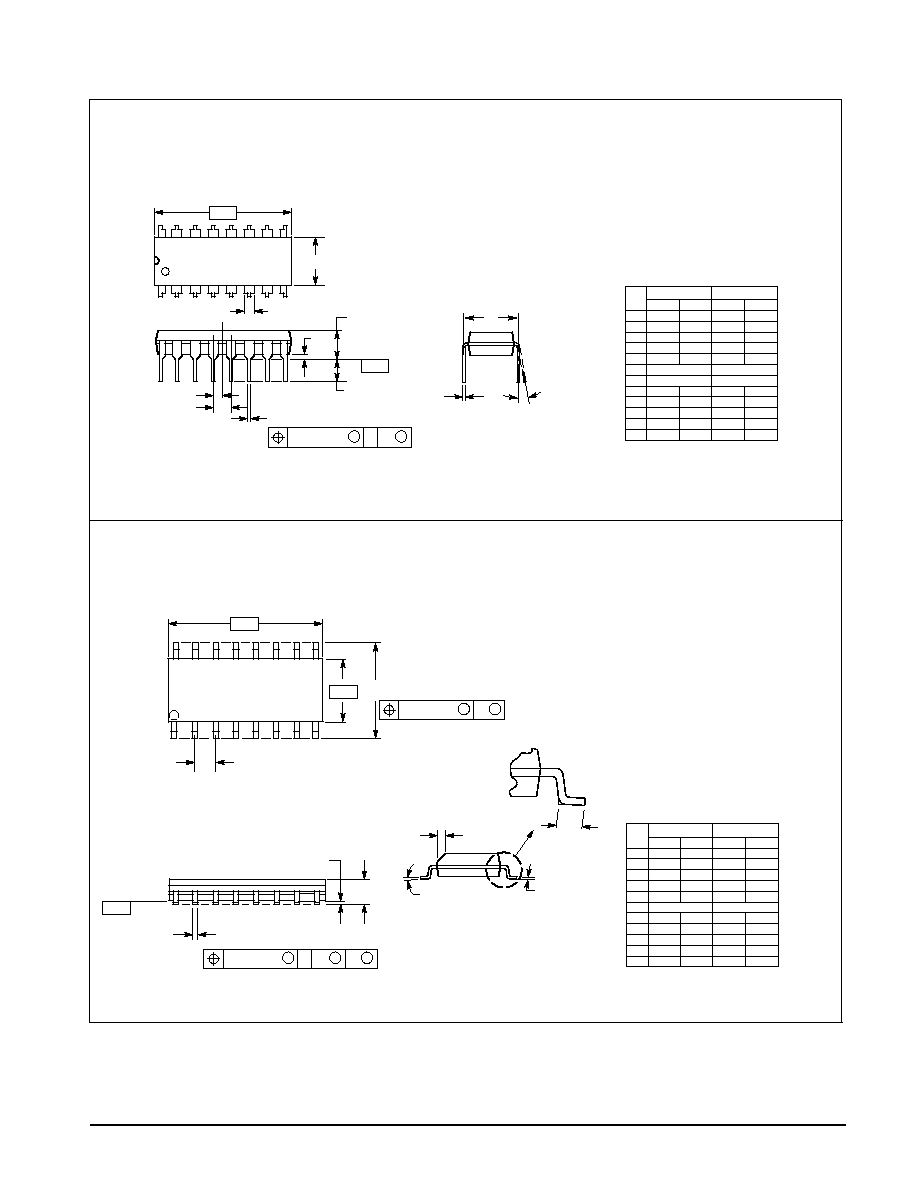
OUTLINE DIMENSIONS
NOTES:
1. DIMENSIONING AND TOLERANCING PER ANSI
Y14.5M, 1982.
2. CONTROLLING DIMENSION: INCH.
3. DIMENSION L TO CENTER OF LEADS WHEN
FORMED PARALLEL.
4. DIMENSION B DOES NOT INCLUDE MOLD FLASH.
5. ROUNDED CORNERS OPTIONAL.
A
B
F
C
S
H
G
D
J
L
M
16 PL
SEATING
1
8
9
16
K
PLANE
T
M
A
M
0.25 (0.010)
T
DIM
MIN
MAX
MIN
MAX
MILLIMETERS
INCHES
A
0.740
0.770
18.80
19.55
B
0.250
0.270
6.35
6.85
C
0.145
0.175
3.69
4.44
D
0.015
0.021
0.39
0.53
F
0.040
0.70
1.02
1.77
G
0.100 BSC
2.54 BSC
H
0.050 BSC
1.27 BSC
J
0.008
0.015
0.21
0.38
K
0.110
0.130
2.80
3.30
L
0.295
0.305
7.50
7.74
M
0
10
0
10
S
0.020
0.040
0.51
1.01
_
_
_
_
NOTES:
1. DIMENSIONING AND TOLERANCING PER ANSI
Y14.5M, 1982.
2. CONTROLLING DIMENSION: MILLIMETER.
3. DIMENSIONS A AND B DO NOT INCLUDE
MOLD PROTRUSION.
4. MAXIMUM MOLD PROTRUSION 0.15 (0.006)
PER SIDE.
5. DIMENSION D DOES NOT INCLUDE DAMBAR
PROTRUSION. ALLOWABLE DAMBAR
PROTRUSION SHALL BE 0.127 (0.005) TOTAL
IN EXCESS OF THE D DIMENSION AT
MAXIMUM MATERIAL CONDITION.
1
8
16
9
SEATING
PLANE
F
J
M
R
X 45
_
G
8 PL
P
B
A
M
0.25 (0.010)
B
S
T
D
K
C
16 PL
S
B
M
0.25 (0.010)
A
S
T
DIM
MIN
MAX
MIN
MAX
INCHES
MILLIMETERS
A
9.80
10.00
0.386
0.393
B
3.80
4.00
0.150
0.157
C
1.35
1.75
0.054
0.068
D
0.35
0.49
0.014
0.019
F
0.40
1.25
0.016
0.049
G
1.27 BSC
0.050 BSC
J
0.19
0.25
0.008
0.009
K
0.10
0.25
0.004
0.009
M
0
7
0
7
P
5.80
6.20
0.229
0.244
R
0.25
0.50
0.010
0.019
_
_
_
_
P SUFFIX
PLASTIC PACKAGE
CASE 64808
ISSUE R
D SUFFIX
PLASTIC PACKAGE
CASE 751B05
(SO16)
ISSUE J

MC3357
6
MOTOROLA ANALOG IC DEVICE DATA
Motorola reserves the right to make changes without further notice to any products herein. Motorola makes no warranty, representation or guarantee regarding
the suitability of its products for any particular purpose, nor does Motorola assume any liability arising out of the application or use of any product or circuit, and
specifically disclaims any and all liability, including without limitation consequential or incidental damages. "Typical" parameters which may be provided in Motorola
data sheets and/or specifications can and do vary in different applications and actual performance may vary over time. All operating parameters, including "Typicals"
must be validated for each customer application by customer's technical experts. Motorola does not convey any license under its patent rights nor the rights of
others. Motorola products are not designed, intended, or authorized for use as components in systems intended for surgical implant into the body, or other
applications intended to support or sustain life, or for any other application in which the failure of the Motorola product could create a situation where personal injury
or death may occur. Should Buyer purchase or use Motorola products for any such unintended or unauthorized application, Buyer shall indemnify and hold Motorola
and its officers, employees, subsidiaries, affiliates, and distributors harmless against all claims, costs, damages, and expenses, and reasonable attorney fees
arising out of, directly or indirectly, any claim of personal injury or death associated with such unintended or unauthorized use, even if such claim alleges that
Motorola was negligent regarding the design or manufacture of the part. Motorola and are registered trademarks of Motorola, Inc. Motorola, Inc. is an Equal
Opportunity/Affirmative Action Employer.
How to reach us:
USA / EUROPE / Locations Not Listed: Motorola Literature Distribution;
JAPAN: Nippon Motorola Ltd.; TatsumiSPDJLDC, 6F SeibuButsuryuCenter,
P.O. Box 20912; Phoenix, Arizona 85036. 18004412447 or 6023035454
3142 Tatsumi KotoKu, Tokyo 135, Japan. 038135218315
MFAX: RMFAX0@email.sps.mot.com TOUCHTONE 6022446609
ASIA/PACIFIC: Motorola Semiconductors H.K. Ltd.; 8B Tai Ping Industrial Park,
INTERNET: http://DesignNET.com
51 Ting Kok Road, Tai Po, N.T., Hong Kong. 85226629298
MC3357/D
*MC3357/D*