 | –≠–ª–µ–∫—Ç—Ä–æ–Ω–Ω—ã–π –∫–æ–º–ø–æ–Ω–µ–Ω—Ç: MC3479P | –°–∫–∞—á–∞—Ç—å:  PDF PDF  ZIP ZIP |

MC3479
SEMICONDUCTOR
TECHNICAL DATA
STEPPER MOTOR
DRIVER
Order this document by MC3479/D
P SUFFIX
PLASTIC PACKAGE
CASE 648C
(Top View)
Bias/Set
Gnd
Gnd
Gnd
Gnd
10
Gnd
4
18
3
9
Gnd
Gnd
1
OIC
Gnd
Clk
Gnd
Bias/Set
16
VM
Gnd
PIN CONNECTIONS
L4
11
12
13
17
16
15
14
8
7
9
2
1
5
19
8
4
20
7
6
5
3
2
L1
L2
Full/Half
Step
VD
CW/CCW
Phase A
L4
L3
15
14
13
12
11
10
6
L3
V
V
L2
L1
M
D
Phase A
CW/CCW
Full/Half Step
OIC
Clk
INPUT TRUTH TABLE
Input Low
Input High
CW
CCW
Full Step
Half Step
Hi Z
Low Z
CW/CCW
Full/Half Step
OIC
Positive Edge Triggered
Clk
1
MOTOROLA ANALOG IC DEVICE DATA
Stepper Motor Driver
The MC3479 is designed to drive a two≠phase stepper motor in the
bipolar mode. The circuit consists of four input sections, a logic
decoding/sequencing section, two driver≠stages for the motor coils, and an
output to indicate the Phase A drive state.
∑
Single Supply Operation: 7.2 to 16.5 V
∑
350 mA/Coil Drive Capability
∑
Clamp Diodes Provided for Back≠EMF Suppression
∑
Selectable CW/CCW and Full/Half Step Operation
∑
Selectable High/Low Output Impedance (Half Step Mode)
∑
TTL/CMOS Compatible Inputs
∑
Input Hysteresis: 400 mV Minimum
∑
Phase Logic Can Be Initialized to Phase A
∑
Phase A Output Drive State Indication (Open≠Collector)
∑
Available in Standard DIP and Surface Mount
CW/CCW
VM
Gnd
Bias/Set
Phase A
Logic
Driver
OIC
Driver
F/H Step
Clk
Clock
Figure 1. Representative Block Diagram
L4
L3
VD
L2
L1
OIC
Full/Half
Step
CW/CCW
ORDERING INFORMATION
Device
Operating
Temperature Range
Package
MC3479P
TA = 0
∞
to +70
∞
C
Plastic
©
Motorola, Inc. 1996
Rev 1
MC3479
2
MOTOROLA ANALOG IC DEVICE DATA
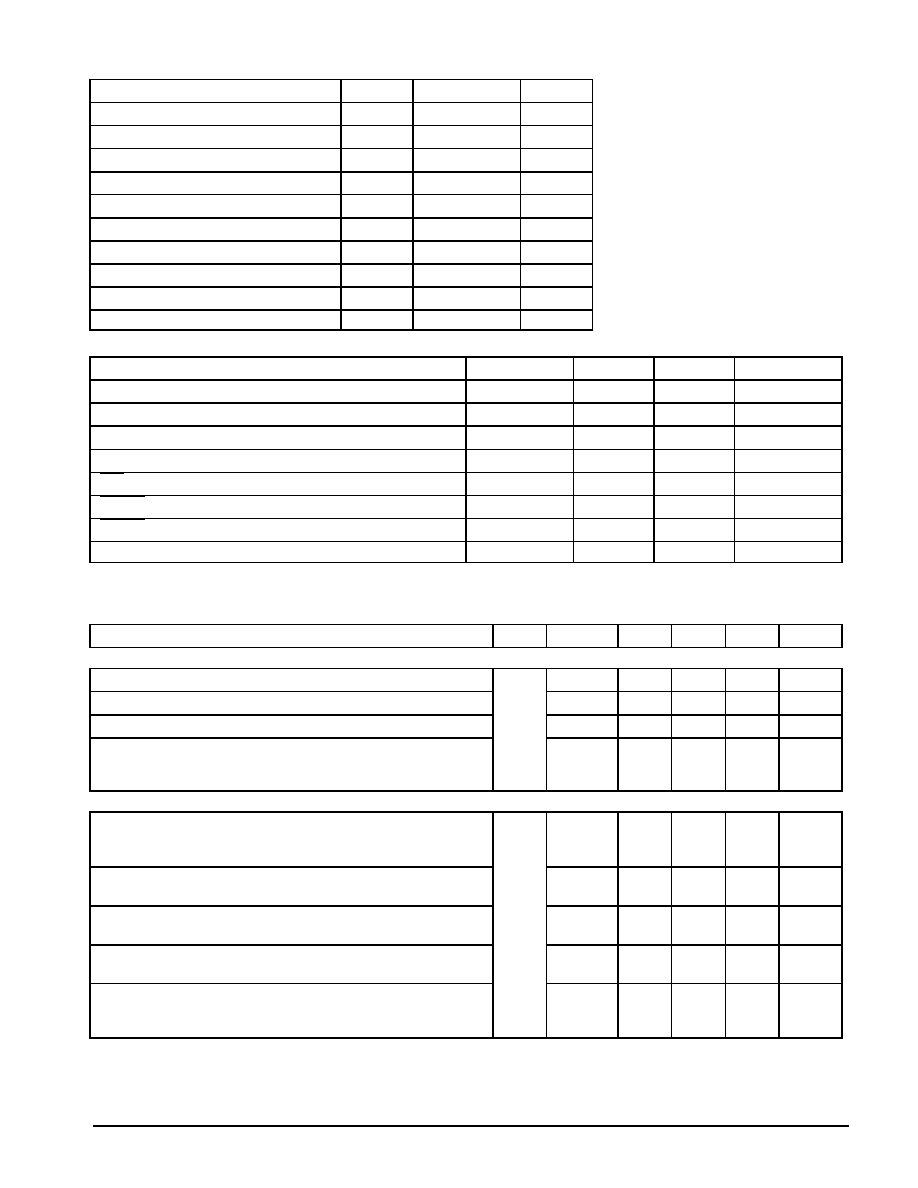
MAXIMUM RATINGS
Rating
Symbol
Value
Unit
Supply Voltage
VM
+ 18
Vdc
Clamp Diode Cathode Voltage (Pin 1)
VD
VM + 5.0
Vdc
Driver Output Voltage
VOD
VM + 6.0
Vdc
Drive Output Current/Coil
IOD
±
500
mA
Input Voltage (Logic Controls)
Vin
≠ 0.5 to + 7.0
Vdc
Bias/Set Current
IBS
≠ 10
mA
Phase A Output Voltage
VOA
+ 18
Vdc
Phase A Sink Current
IOA
20
mA
Junction Temperature
TJ
+ 150
∞
C
Storage Temperature Range
Tstg
≠ 65 to + 150
∞
C
RECOMMENDED OPERATING CONDITIONS
Characteristic
Symbol
Min
Max
Unit
Supply Voltage
VM
+ 7.2
+ 16.5
Vdc
Clamp Diode Cathode Voltage
VD
VM
VM + 4.5
Vdc
Driver Output Current (Per Coil) (Note 1)
IOD
--
350
mA
Input Voltage (Logic Controls)
Vin
0
+ 5.5
Vdc
Bias/Set Current (Outputs Active)
IBS
≠ 300
≠ 75
µ
A
Phase A Output Voltage
VOA
--
VM
Vdc
Phase A Sink Current
IOA
0
8.0
mA
Operating Ambient Temperature
TA
0
+ 70
∞
C
NOTE: 1. See section on Power Dissipation in Application Information.
DC ELECTRICAL CHARACTERISTICS
(Specifications apply over the recommended supply voltage and temperature range, [Notes
2, 3] unless otherwise noted.)
Characteristic
Pins
Symbol
Min
Typ
Max
Unit
INPUT LOGIC LEVELS
Threshold Voltage (Low≠to≠High)
7, 8,
9 10
VTLH
--
--
2.0
Vdc
Threshold Voltage (High≠to≠Low)
9, 10
VTHL
0.8
--
--
Vdc
Hysteresis
VHYS
0.4
--
--
Vdc
Current: (VI = 0.4 V)
Current:
(VI = 5.5 V)
Current:
(VI = 2.7 V)
IIL
≠ 100
--
--
--
--
--
--
+ 100
+ 20
µ
A
DRIVER OUTPUT LEVELS
Output High Voltage
2, 3,
VOHD
Vdc
(IBS = ≠ 300
µ
A): (IOD = ≠ 350 mA)
(IBS = ≠ 300
µ
A):
(IOD = ≠ 0.1 mA)
14, 15
VM ≠ 2.0
VM ≠ 1.2
--
--
--
--
Output Low Voltage
VOLD
--
--
0.8
Vdc
(IBS = ≠ 300
µ
A, IOD = 350 mA)
Differential Mode Output Voltage Difference (Note 4)
DVOD
--
--
0.15
Vdc
(IBS = ≠ 300
µ
A, IOD = 350 mA)
Common Mode Output Voltage Difference (Note 5)
CVOD
--
--
0.15
Vdc
(IBS = ≠ 300
µ
A, IOD = ≠ 0.1 mA)
Output Leakage, Hi Z State
µ
A
(0
p
VOD
p
VM, IBS = ≠ 5.0
µ
A)
IOZ1
≠ 100
--
+ 100
(0
p
VOD
p
VM, IBS = ≠ 300
µ
A, F/H = 2.0 V, OIC = 0.8 V)
IOZ2
≠ 100
--
+ 100
NOTES: 2. Algebraic convention rather than absolute values is used to designate limit values.
3. Current into a pin is designated as positive. Current out of a pin is designated as negative.
4. DVOD =
VOD1,2 ≠ VOD3,4
where: VOD1,2 = (VOHD1 ≠ VOLD2) or (VOHD2 ≠ VOLD1), and
VOD3,4 = (VOHD3 ≠ VOLD4) or (VOHD4 ≠ VOLD3).
5. CVOD =
VOHD1 ≠ VOHD2
or
VOHD3 ≠ VOHD4
.

MC3479
3
MOTOROLA ANALOG IC DEVICE DATA
DC ELECTRICAL CHARACTERISTICS
(Specifications apply over the recommended supply voltage and temperature range, [Notes
2, 3] unless otherwise noted.)
Characteristic
Pins
Symbol
Min
Typ
Max
Unit
CLAMP DIODES
Forward Voltage
1, 2, 3,
VDF
--
2.5
3.0
Vdc
(ID = 350 mA)
14, 15
Leakage Current (Per Diode)
IDR
--
--
100
µ
A
(Pin 1 = 21 V; Outputs = 0 V; IBS = 0
µ
A)
PHASE A OUTPUT
Output Low Voltage
11
VOLA
--
--
0.4
Vdc
(IOA = 8.0 mA)
Off State Leakage Current
IOHA
--
--
100
µ
A
(VOHA = 16.5 V)
POWER SUPPLY
Power Supply Current
16
mA
(IOD = 0
µ
A, IBS = ≠ 300
µ
A)
(L1 = VOHD, L2 = VOLD, L3 = VOHD, L4 = VOLD)
IMW
--
--
70
(L1 = VOHD, L2 = VOLD, L3 = Hi Z, L4 = Hi Z)
IMZ
--
--
40
(L1 = VOHD, L2 = VOLD, L3 = VOHD, L4 = VOHD)
IMN
--
--
75
BIAS/SET CURRENT
To Set Phase A
6
IBS
≠ 5.0
--
--
µ
A
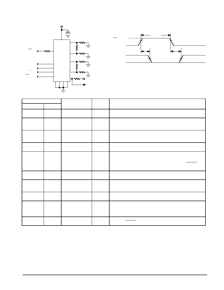
PACKAGE THERMAL CHARACTERISTICS
Characteristic
Symbol
Min
Typ
Max
Unit
Thermal Resistance, Junction≠to≠Ambient (No Heatsink)
R
JA
--
45
--
∞
C/W
AC SWITCHING CHARACTERISTICS
(TA = + 25
∞
C, VM = 12 V) (See Figures 2, 3, 4)
Characteristic
Pins
Symbol
Min
Typ
Max
Unit
Clock Frequency
7
fCK
0
--
50
kHz
Clock Pulse Width (High)
7
PWCKH
10
--
--
µ
s
Clock Pulse Width (Low)
7
PWCKL
10
--
--
µ
s
Bias/Set Pulse Width
6
PWBS
10
--
--
µ
s
Setup Time (CW/CCW and F/HS)
10≠7
9≠7
tsu
5.0
--
--
µ
s
Hold Time (CW/CCW and F/HS)
10≠7
9≠7
th
10
--
--
µ
s
Propagation Delay (Clk≠to≠Driver Output)
tPCD
--
8.0
--
µ
s
Propagation Delay (Bias/Set≠to≠Driver Output)
tPBSD
--
1.0
--
µ
s
Propagation Delay (Clk≠to≠Phase A Low)
7≠11
tPHLA
--
12
--
µ
s
Propagation Delay (Clk≠to≠Phase A High)
7≠11
tPLHA
--
5.0
--
µ
s
NOTES: 2. Algebraic convention rather than absolute values is used to designate limit values.
3. Current into a pin is designated as positive. Current out of a pin is designated as negative.
MC3479
4
MOTOROLA ANALOG IC DEVICE DATA
5
Phase A
+ 12 V
MC3479P
CW / CCW
F / HS
OIC
Clk
Bias/Set
56 k
6
7
8
9
10
4
12 13
15
14
3
2
16
VM
1.0 k
1.0 k
1.0 k
1.0 k
1.0 k
1.0 k
4.0 k
11
L3
L4
L1
L2
0.1
µ
F
+ 12 V
Figure 2. AC Test Circuit
Note: tr, tf (10% to 90%) for
input signals are
p
25 ns.
Figure 3. Bias/Set Timing
(Refer to Figure 2)
Bias/Set
Input
VM
PWBS
VM ≠ 1.0
VM ≠ 1.0
tPBSD
tPBSD
(High Impedance)
0
L1 ≠ L4
Outputs
PIN FUNCTION DESCRIPTION
Pin No.
20≠Pin
16≠Pin
Function
Symbol
Description
20
16
Power Supply
VM
Power supply pin for both the logic circuit and the motor coil current.
Voltage range is + 7.2 to + 16.5 volts.
4, 5, 6, 7,
14, 15, 16, 17
4, 5,
12, 13
Ground
Gnd
Ground pins for the logic circuit and the motor coil current. The
physical configuration of the pins aids in dissipating heat from within
the IC package.
1
1
Clamp Diode
Voltage
VD
This pin is used to protect the outputs where large voltage spikes may
occur as the motor coils are switched. Typically a diode is connected
between this pin and Pin 16. See Figure 11.
2, 3,
18, 19
2, 3,
14, 15
Driver Outputs
L1, L2
L3, L4
High current outputs for the motor coils. L1 and L2 are connected to
one coil, and L3 and L4 to the other coil.
8
6
Bias/Set
B/S
This pin is typically 0.7 volts below VM. The current out of this pin
(through a resistor to ground) determines the maximum output sink
current. If the pin is opened (IBS < 5.0
µ
A) the outputs assume a high
impedance condition, while the internal logic presets to a Phase A
condition.
9
7
Clock
Clk
The positive edge of the clock input switches the outputs to the next
position. This input has no effect if Pin 6 is open.
11
9
Full/Half Step
F/HS
When low (Logic "0"), each clock input pulse will cause the motor to
rotate one full step. When high, each clock pulse will cause the motor
to rotate one≠half step. See Figure 7 for sequence.
12
10
Clockwise/
Counterclockwise
CW/CCW
This input allows reversing the rotation of the motor. See Figure 7 for
sequence.
10
8
Output Impedance
Control
OIC
This input is relevant only in the half step mode (Pin 9 > 2.0 V). When
low (Logic "0"), the two driver outputs of the non≠energized coil will be
in a high impedance condition. When high the same driver outputs will
be at a low impedance referenced to VM. See Figure 7.
13
11
Phase A
Ph A
This open≠collector output indicates (when low) that the driver outputs
are in the Phase A condition (L1 = L3 = VOHD, L2 = L4 = VOLD).
APPLICATION INFORMATION
General
The MC3479 integrated circuit is designed to drive a
stepper positioning motor in applications such as disk drives
and robotics. The outputs can provide up to 350 mA to each
of two coils of a two≠phase motor. The outputs change state
with each low≠to≠high transition of the clock input, with the
new output state depending on the previous state, as well as
the input conditions at the logic controls.
Outputs
The outputs (L1≠L4) are high current outputs (see
Figure 5), which when connected to a two≠phase motor,
provide two full≠bridge configurations (L3 and L4 are not
shown in Figure 5). The polarities applied to the motor coils
depend on which transistor (QH or QL) of each output is on,
which in turn depends on the inputs and the decoding
circuitry.
MC3479
5
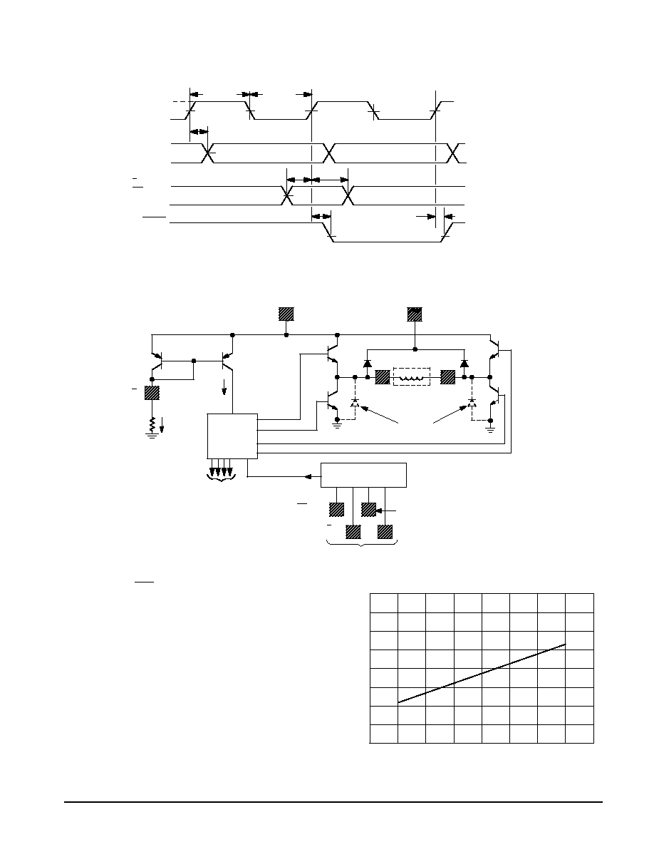
MOTOROLA ANALOG IC DEVICE DATA
Note: tr, tf (10% to 90%) for input
signals are
p
10 ns.
tPLHA
tPHLA
th
tsu
PWCLKL
PWCLKH
1.5 V
1.5 V
Phase A
Output
F/HS,
CW/CCW
Inputs
0
L1 ≠ L4
Outputs
tPCD
3.0 V
0
Clk
3.0 V
Figure 4. Clock Timing
(Refer to Figure 2)
6.0 V
1.5 V
Current
Drivers
and
Logic
VD
QH
QL
L2
Parasitic
Diodes
L1
Motor Coil
QL
VM
B/S
I
BS
IBS
RB
To L3, L4
Transistors
CW / CCW
OIC
Clk
F/HS
Inputs
Logic Decoding
Circuit
Figure 5. Output Stages
QH
The maximum sink current available at the outputs is a
function of the resistor connected between Pin 6 and ground
(see section on Bias/Set operation). Whenever the outputs
are to be in a high impedance state, both transistors (QH and
QL of Figure 5) of each output are off.
VD
This pin allows for provision of a current path for the motor
coil current during switching, in order to suppress back≠EMF
voltage spikes. VD is normally connected to VM (Pin 16)
through a diode (zener or regular), a resistor, or directly. The
peaks instantaneous voltage at the outputs must not exceed
VM by more than 6.0 V. The voltage drop across the internal
clamping diodes must be included in this portion of the design
(see Figure 6). Note the parasitic diodes (Figure 5) across
each QL of each output provide for a complete circuit path for
the switched current.
Figure 6. Clamp Diode Characteristics
ID (mA)
300
100
200
0
0
1.0
2.0
3.0
V (V)
F