 | ÐлекÑÑоннÑй компоненÑ: MC3487D | СкаÑаÑÑ:  PDF PDF  ZIP ZIP |
Äîêóìåíòàöèÿ è îïèñàíèÿ www.docs.chipfind.ru
Device
Operating
Temperature Range
Package
MC3487
SEMICONDUCTOR
TECHNICAL DATA
QUAD EIA422 LINE DRIVER
WITH THREESTATE
OUTPUTS
ORDERING INFORMATION
MC3487P
MC3487D
TA = 0 to +70
°
C
Plastic DIP
SO16
PIN CONNECTIONS
Order this document by MC3487/D
P SUFFIX
PLASTIC PACKAGE
CASE 648
D SUFFIX
PLASTIC PACKAGE
CASE 751B
(SO16)
10
11
13
14
Outputs B
Outputs A
2
3
5
6
Outputs C
Outputs D
VCC
Input D
C/D Control
Input C
9
8
7
1
4
Gnd
Input B
A/B Control
12
15
16
Input A
1
MOTOROLA ANALOG IC DEVICE DATA
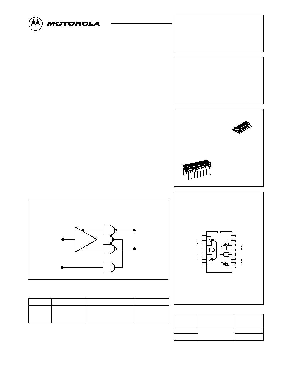
Quad Line Driver with
Three-State Outputs
Motorola
i
s Quad EIA422 Driver features four independent driver chains
which comply with EIA Standards for the Electrical Characteristics of
Balanced Voltage Digital Interface Circuits. The outputs are threestate
structures which are forced to a high impedance state when the appropriate
output control pin reaches a logic zero condition. All input pins are PNP
buffered to minimize input loading for either logic one or logic zero inputs. In
addition, internal circuitry assures a high impedance output state during the
transition between power up and power down. A summary of MC3487
features include:
·
Four Independent Driver Chains
·
ThreeState Outputs
·
PNP High Impedance Inputs (PIA Compatible)
·
Fast Propagation Times (Typical 15 ns)
·
TTL Compatible
·
Single 5.0 V Supply Voltage
·
Output Rise and Fall Times Less Than 20 ns
·
DS 3487 Provides Second Source
Driver Block Diagram
Input
NonInverting
Inverting
Output
Control
Outputs
TRUTH TABLE
Input
Control Input
NonInverting Output
Inverting Output
H
H
H
L
L
H
L
H
X
L
Z
Z
L = Low Logic State
H = High Logic State
X = Irrelevant
Z = ThirdState (High Impedance)
©
Motorola, Inc. 1995
MC3487
2
MOTOROLA ANALOG IC DEVICE DATA
MAXIMUM RATINGS
Rating
Symbol
Value
Unit
Power Supply Voltage
VCC
8.0
Vdc
Input Voltage
VI
5.5
Vdc
Operating Ambient Temperature Range
TA
0 to +70
°
C
Operating Junction Temperature Range
TJ
150
°
C
Storage Temperature Range
Tstg
65 to +150
°
C
ELECTRICAL CHARACTERISTICS
(Unless otherwise noted, specifications apply 4.75 V
p
VCC
p
5.25 V and 0
°
C
p
TA
p
70
°
C.
Typical values measured at VCC = 5.0 V, and TA = 25
°
C.)
Characteristic
Symbol
Min
Typ
Max
Unit
Input Voltage Low Logic State
VIL
0.8
Vdc
Input Voltage High Logic State
VIH
2.0
Vdc
Input Current Low Logic State
(VIL = 0.5 V)
IIL
400
µ
A
Input Current High Logic State
(VIH = 2.7 V)
(VIH = 5.5 V)
IIH
+ 50
+ 100
µ
A
Input Clamp Voltage
(IIK = 18 mA)
VIK
1.5
V
Output Voltage Low Logic State
(IOL = 48 mA)
VOL
0.5
V
Output Voltage High Logic State
(IOH = 20 mA)
VOH
2.5
V
Output ShortCircuit Current
(VIH = 2.0 V, Note 1)
IOS
40
140
mA
Output Leakage Current HiZ State
(VIL = 0.5 V, VIL(Z) = 0.8 V)
(VIH = 2.7 V, VIL(Z) = 0.8 V)
IOL(Z)
±
100
±
100
µ
A
Output Leakage Current Power OFF
(VOH = 6.0 V, VCC = 0 V)
(VOL = 0.25 V, VCC = 0 V)
IOL(off)
+ 100
100
µ
A
Output Offset Voltage Difference (Note 2)
VOS VOS
±
0.4
V
Output Differential Voltage (Note 2)
VOD
2.0
V
Output Differential Voltage Difference (Note 2)
VOD
±
0.4
V
Power Supply Current
(Control Pins = Gnd, Note 3)
(Control Pins = 2.0 V)
ICCX
ICC
105
85
mA
NOTES: 1. Only one output may be shorted at a time.
2. See EIA Specification EIA422 for exact test conditions.
3. Circuit in threestate condition.
SWITCHING CHARACTERISTICS
(VCC = 5.0 V, TA = 25
°
C, unless otherwise noted.)
Characteristic
Symbol
Min
Typ
Max
Unit
Propagation Delay Times
High to Low Output
Low to High Output
tPHL
tPLH
20
20
ns
Output Transition Times Differential
High to Low Output
Low to High Output
tTHL
tTLH
20
20
ns
Propagation Delay Control to Output
(RL = 200
, CL = 50 pF)
(RL = 200
, CL = 50 pF)
(RL =
, CL = 50 pF)
(RL = 200
, CL = 50 pF)
tPHZ(E)
tPLZ(E)
tPZH(E)
tPZL(E)
25
25
30
30
ns
MC3487
3
MOTOROLA ANALOG IC DEVICE DATA
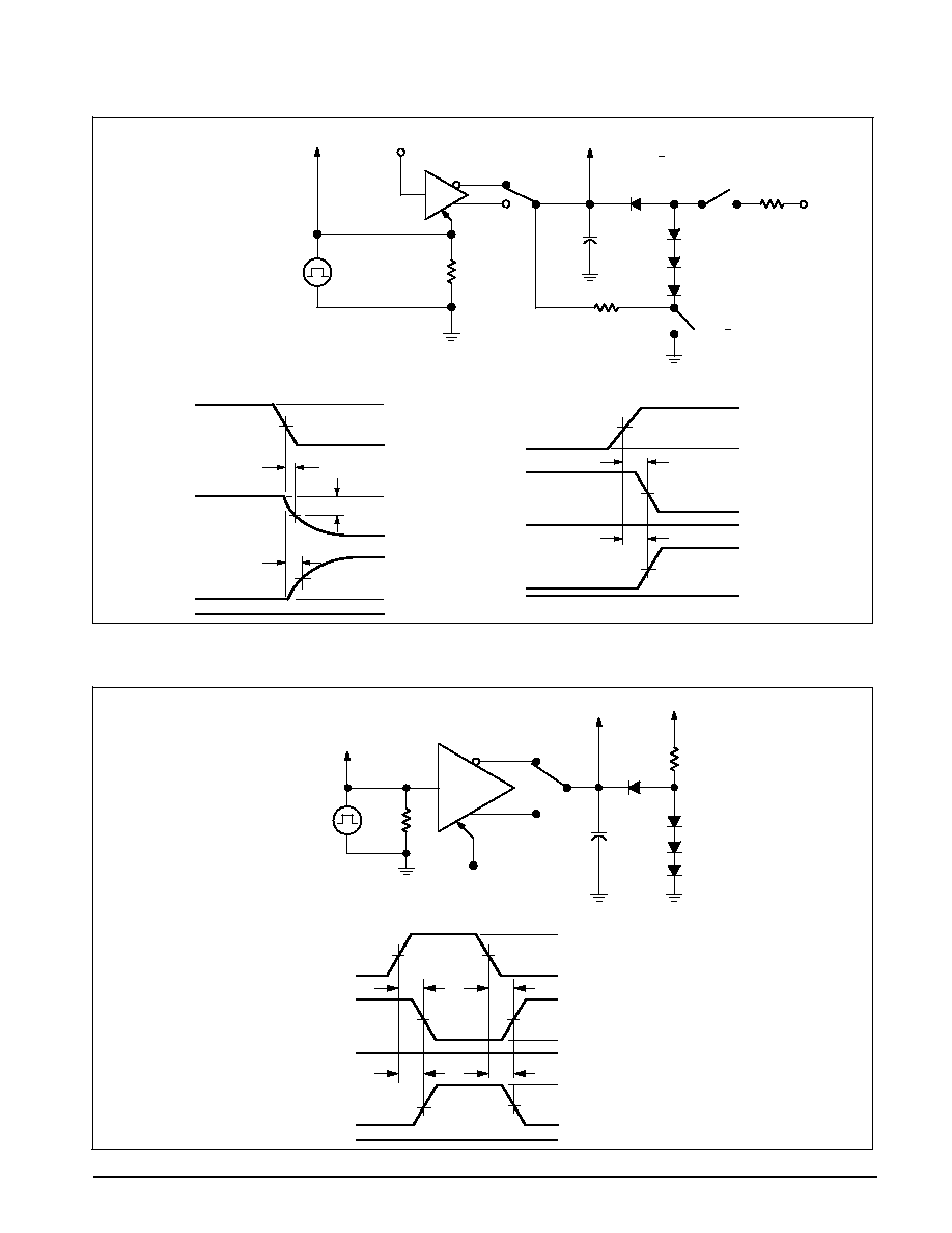
Control
Input
1.5 V
tPHZ(E)
0.5 V
0.5 V
VOH
p
1.5 V
1.5 V
VOL
0 V
tPLZ(E)
0
Output
Output
CL
50 pF
Open for
tPZL(E) Test Only
1.0 k
200
To Scope
Output
Open for tPZH(E) Test Only
5.0 V
1N3064
or Equivalent
3.0 V or Gnd
Input
CL Includes Probe and
Jig Capacitance
3.0 V
Inv
Output
To Scope (Input)
NonInv
Output
50
Control
Pulse
Generator
Pulse generator characteristics
Zo = 50
PRR = 1.0 MHz
50% Duty Cycle
tTLH, tTHL
p
5 ns
VOH
0 V
0 V
tPZH(E)
0
VOL
Output
Output
Control
Input
1.5 V
3.0 V
1.5 V
1.5 V
tPZL(E)
CL includes probe
and jig capacitance
Input
Output
tPHL
3.0 V
tPLH
Output
tPLH
1.5 V
tPHL
0 V
VOH
VOL
0 V
1.5 V
0 V
VOH
1.5 V
1.5 V
1.5 V
1.5 V
1N914 or
Equivalent
Scope
(Output)
CL = 50 pF
1/4
MC3487
Inv
Output
NonInv
Output
Control
3.0 V
Scope
(Input)
Pulse
Generator
51
5.0 V
RL = 200
VOL
Pulse generator characteristics
Zo = 50
PRR = 1.0 MHz
50% Duty Cycle
tTLH, tTHL
p
5 ns
Figure 1. ThreeState Enable Test Circuit
and Waveforms
Figure 2. Propagation Delay Times Input to
Output Waveforms and Test Circuit
MC3487
4
MOTOROLA ANALOG IC DEVICE DATA
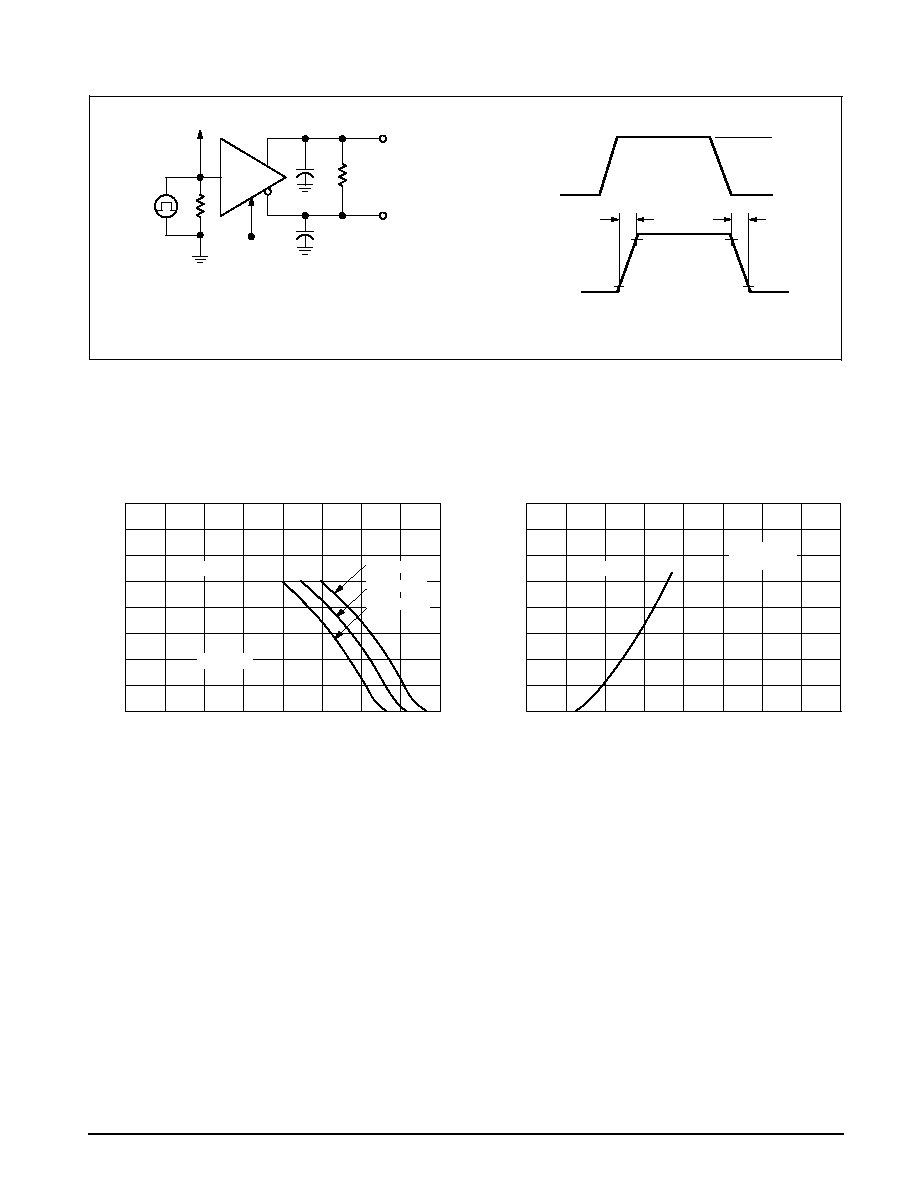
Figure 3. Output Transition Times Test Circuit and Waveforms
Scope
Output
(Differential)
CL
CL includes probe
and jig capacitance
CL
15 pF
51
3.0 V
Scope
Input
1/4
MC3487
Output
(Differential)
3.0 V
90%
tTLH
10%
Input
0 V
RL =
100
tTHL
Pulse generator characteristics
Zo = 50
PRR = 1.0 MHz
50% Duty Cycle
tTLH, tTHL
p
5 ns
VOL, OUTPUT VOLTAGE LOW (mV)
0
VCC = 5.0 V
TA = 25
°
C
700
500
100
(Typical)
300
200
400
20
30
40
50
10
60
70
0
80
0
4.0
1.0
3.0
(Typical)
2.0
TA = 25
°
C
VCC = 5.25 V
VOH, OUTPUT VOLTAGE (V)
20
30
40
50
600
800
VCC = 5.0 V
VCC = 4.75 V
80
0
70
60
10
, OUTPUT
CURRENT
(mA)
I OH
, OUTPUT
SINK CURRENT
LOW (mA)
I OL
Figure 4. Output Current versus Output Voltage
Figure 5. Output Sink Current versus
Output Voltage
MC3487
5
MOTOROLA ANALOG IC DEVICE DATA
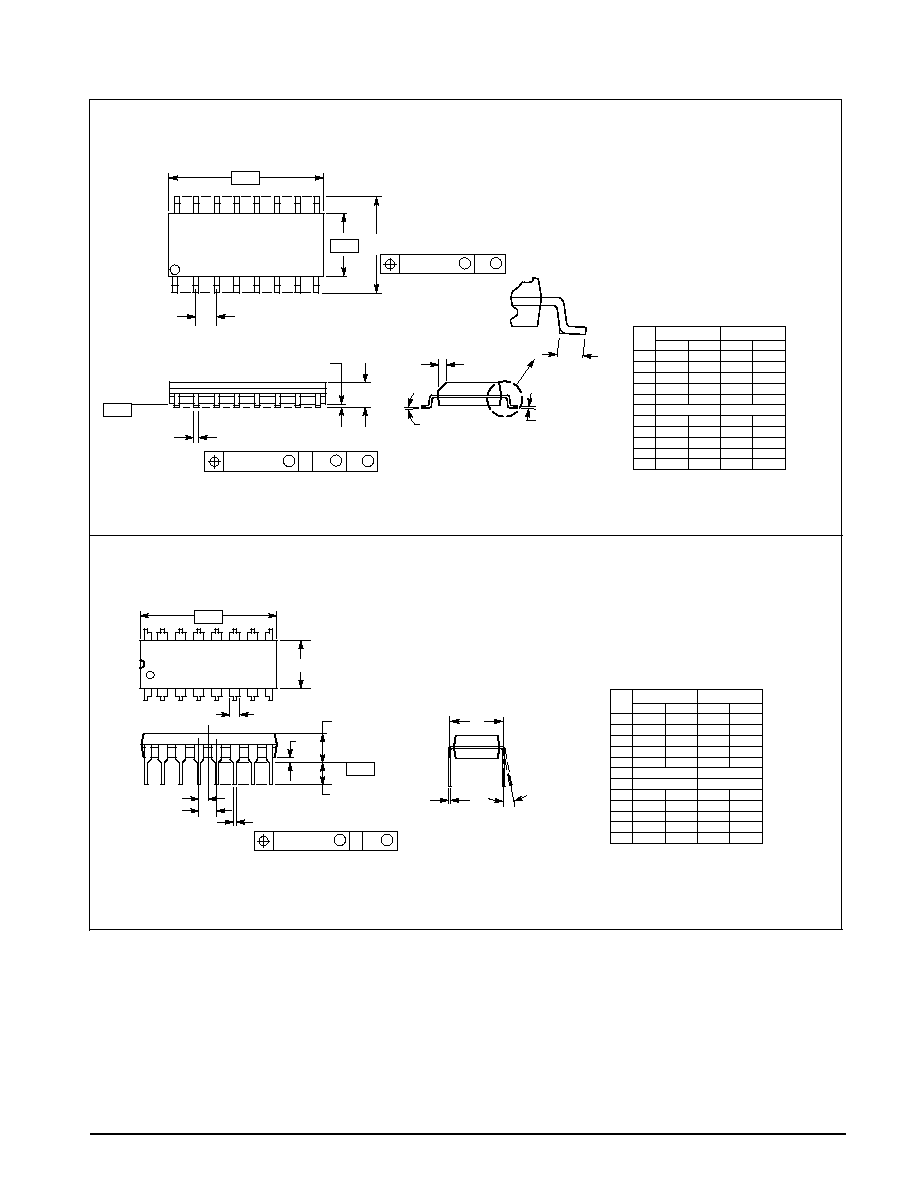
OUTLINE DIMENSIONS
NOTES:
1. DIMENSIONING AND TOLERANCING PER ANSI
Y14.5M, 1982.
2. CONTROLLING DIMENSION: INCH.
3. DIMENSION L TO CENTER OF LEADS WHEN
FORMED PARALLEL.
4. DIMENSION B DOES NOT INCLUDE MOLD FLASH.
5. ROUNDED CORNERS OPTIONAL.
A
B
F
C
S
H
G
D
J
L
M
16 PL
SEATING
1
8
9
16
K
PLANE
T
M
A
M
0.25 (0.010)
T
DIM
MIN
MAX
MIN
MAX
MILLIMETERS
INCHES
A
0.740
0.770
18.80
19.55
B
0.250
0.270
6.35
6.85
C
0.145
0.175
3.69
4.44
D
0.015
0.021
0.39
0.53
F
0.040
0.70
1.02
1.77
G
0.100 BSC
2.54 BSC
H
0.050 BSC
1.27 BSC
J
0.008
0.015
0.21
0.38
K
0.110
0.130
2.80
3.30
L
0.295
0.305
7.50
7.74
M
0
10
0
10
S
0.020
0.040
0.51
1.01
_
_
_
_
NOTES:
1. DIMENSIONING AND TOLERANCING PER ANSI
Y14.5M, 1982.
2. CONTROLLING DIMENSION: MILLIMETER.
3. DIMENSIONS A AND B DO NOT INCLUDE
MOLD PROTRUSION.
4. MAXIMUM MOLD PROTRUSION 0.15 (0.006)
PER SIDE.
5. DIMENSION D DOES NOT INCLUDE DAMBAR
PROTRUSION. ALLOWABLE DAMBAR
PROTRUSION SHALL BE 0.127 (0.005) TOTAL
IN EXCESS OF THE D DIMENSION AT
MAXIMUM MATERIAL CONDITION.
1
8
16
9
SEATING
PLANE
F
J
M
R
X 45
_
G
8 PL
P
B
A
M
0.25 (0.010)
B
S
T
D
K
C
16 PL
S
B
M
0.25 (0.010)
A
S
T
DIM
MIN
MAX
MIN
MAX
INCHES
MILLIMETERS
A
9.80
10.00
0.386
0.393
B
3.80
4.00
0.150
0.157
C
1.35
1.75
0.054
0.068
D
0.35
0.49
0.014
0.019
F
0.40
1.25
0.016
0.049
G
1.27 BSC
0.050 BSC
J
0.19
0.25
0.008
0.009
K
0.10
0.25
0.004
0.009
M
0
7
0
7
P
5.80
6.20
0.229
0.244
R
0.25
0.50
0.010
0.019
_
_
_
_
P SUFFIX
PLASTIC PACKAGE
CASE 64808
ISSUE R
D SUFFIX
PLASTIC PACKAGE
CASE 751B05
(SO16)
ISSUE J

MC3487
6
MOTOROLA ANALOG IC DEVICE DATA
Motorola reserves the right to make changes without further notice to any products herein. Motorola makes no warranty, representation or guarantee regarding
the suitability of its products for any particular purpose, nor does Motorola assume any liability arising out of the application or use of any product or circuit,
and specifically disclaims any and all liability, including without limitation consequential or incidental damages. "Typical" parameters can and do vary in different
applications. All operating parameters, including "Typicals" must be validated for each customer application by customer's technical experts. Motorola does
not convey any license under its patent rights nor the rights of others. Motorola products are not designed, intended, or authorized for use as components in
systems intended for surgical implant into the body, or other applications intended to support or sustain life, or for any other application in which the failure of
the Motorola product could create a situation where personal injury or death may occur. Should Buyer purchase or use Motorola products for any such
unintended or unauthorized application, Buyer shall indemnify and hold Motorola and its officers, employees, subsidiaries, affiliates, and distributors harmless
against all claims, costs, damages, and expenses, and reasonable attorney fees arising out of, directly or indirectly, any claim of personal injury or death
associated with such unintended or unauthorized use, even if such claim alleges that Motorola was negligent regarding the design or manufacture of the part.
Motorola and
are registered trademarks of Motorola, Inc. Motorola, Inc. is an Equal Opportunity/Affirmative Action Employer.
How to reach us:
USA / EUROPE: Motorola Literature Distribution;
JAPAN: Nippon Motorola Ltd.; TatsumiSPDJLDC, Toshikatsu Otsuki,
P.O. Box 20912; Phoenix, Arizona 85036. 18004412447
6F SeibuButsuryuCenter, 3142 Tatsumi KotoKu, Tokyo 135, Japan. 0335218315
MFAX: RMFAX0@email.sps.mot.com TOUCHTONE (602) 2446609
HONG KONG: Motorola Semiconductors H.K. Ltd.; 8B Tai Ping Industrial Park,
INTERNET: http://DesignNET.com
51 Ting Kok Road, Tai Po, N.T., Hong Kong. 85226629298
MC3487/D
*MC3487/D*