ƒÓÍÛÏÂÌÚýˆËˇ Ë ÓÔËÒýÌˡ www.docs.chipfind.ru

MC68HC705KJ1/D
Rev. 2.0
MC68HC705KJ1
MC68HSC705KJ1
MC68HRC705KJ1
MC68HLC705KJ1
HCMOS Microcontroller Unit
TECHNICAL DATA BOOK
HC 5

Technical Data
MC68HC705KJ1 -- Rev. 2.0
2
Technical Data
MOTOROLA
Technical Data
Motorola reserves the right to make changes without further notice to
any products herein to improve reliability, function or design. Motorola
does not assume any liability arising out of the application or use of any
product or circuit described herein; neither does it convey any license
under its patent rights nor the rights of others. Motorola products are not
designed, intended, or authorized for use as components in systems
intended for surgical implant into the body, or other applications intended
to support or sustain life, or for any other application in which the failure
of the Motorola product could create a situation where personal injury or
death may occur. Should Buyer purchase or use Motorola products for
any such unintended or unauthorized application, Buyer shall indemnify
and hold Motorola and its officers, employees, subsidiaries, affiliates,
and distributors harmless against all claims, costs, damages, and
expenses, and reasonable attorney fees arising out of, directly or
indirectly, any claim of personal injury or death associated with such
unintended or unauthorized use, even if such claim alleges that Motorola
was negligent regarding the design or manufacture of the part.
© Motorola, Inc., 2000

MC68HC705KJ1 -- Rev. 2.0
Technical Data
MOTOROLA
List of Sections
3
Technical Data -- MC68HC705KJ1
List of Sections
Section 1. Introduction . . . . . . . . . . . . . . . . . . . . . . . . . . . 19
Section 2. Pin Descriptions . . . . . . . . . . . . . . . . . . . . . . . 23
Section 3. Memory . . . . . . . . . . . . . . . . . . . . . . . . . . . . . . 31
Section 4. Central Processor Unit (CPU) . . . . . . . . . . . . 41
Section 5. Resets and Interrupts . . . . . . . . . . . . . . . . . . . 63
Section 6. Low-Power Modes. . . . . . . . . . . . . . . . . . . . . . 73
Section 7. Parallel I/O Ports . . . . . . . . . . . . . . . . . . . . . . . 81
Section 8. Computer Operating Properly
Module (COP) . . . . . . . . . . . . . . . . . . . . . . . . . 93
Section 9. External Interrupt Module (IRQ) . . . . . . . . . . . 97
Section 10. Multifunction Timer Module . . . . . . . . . . . . 105
Section 11. Electrical Specifications . . . . . . . . . . . . . . . 113
Section 12. Mechanical Specifications . . . . . . . . . . . . . 127
Section 13. Ordering Information . . . . . . . . . . . . . . . . . 131
Appendix A. MC68HRC705KJ1 . . . . . . . . . . . . . . . . . . . 133
Appendix B. MC68HLC705KJ1. . . . . . . . . . . . . . . . . . . . 139

Technical Data
MC68HC705KJ1 -- Rev. 2.0
4
List of Sections
MOTOROLA
List of Sections

MC68HC705KJ1 -- Rev. 2.0
Technical Data
MOTOROLA
Table of Contents
5
Technical Data -- MC68HC705KJ1
Table of Contents
Section 1. Introduction
1.1
Contents . . . . . . . . . . . . . . . . . . . . . . . . . . . . . . . . . . . . . . . . . .19
1.2
Features . . . . . . . . . . . . . . . . . . . . . . . . . . . . . . . . . . . . . . . . . .19
1.3
Structure . . . . . . . . . . . . . . . . . . . . . . . . . . . . . . . . . . . . . . . . . .21
1.4
Programmable Options. . . . . . . . . . . . . . . . . . . . . . . . . . . . . . .22
Section 2. Pin Descriptions
2.1
Contents . . . . . . . . . . . . . . . . . . . . . . . . . . . . . . . . . . . . . . . . . .23
2.2
Pin Assignments . . . . . . . . . . . . . . . . . . . . . . . . . . . . . . . . . . . .24
2.3
Pin Functions . . . . . . . . . . . . . . . . . . . . . . . . . . . . . . . . . . . . . .24
2.3.1
V
DD
and V
SS
. . . . . . . . . . . . . . . . . . . . . . . . . . . . . . . . . . . . .24
2.3.2
OSC1 and OSC2 . . . . . . . . . . . . . . . . . . . . . . . . . . . . . . . . .25
2.3.2.1
Crystal Oscillator . . . . . . . . . . . . . . . . . . . . . . . . . . . . . . .25
2.3.2.2
Ceramic Resonator Oscillator . . . . . . . . . . . . . . . . . . . . .26
2.3.2.3
RC Oscillator . . . . . . . . . . . . . . . . . . . . . . . . . . . . . . . . . .28
2.3.2.4
External Clock . . . . . . . . . . . . . . . . . . . . . . . . . . . . . . . . .28
2.3.3
RESET . . . . . . . . . . . . . . . . . . . . . . . . . . . . . . . . . . . . . . . . .28
2.3.4
IRQ/V
PP
. . . . . . . . . . . . . . . . . . . . . . . . . . . . . . . . . . . . . . . .29
2.3.5
PA0≠PA7 . . . . . . . . . . . . . . . . . . . . . . . . . . . . . . . . . . . . . . .29
2.3.6
PB2 and PB3 . . . . . . . . . . . . . . . . . . . . . . . . . . . . . . . . . . . .29

Technical Data
MC68HC705KJ1 -- Rev. 2.0
6
Table of Contents
MOTOROLA
Table of Contents
Section 3. Memory
3.1
Contents . . . . . . . . . . . . . . . . . . . . . . . . . . . . . . . . . . . . . . . . . .31
3.2
Features . . . . . . . . . . . . . . . . . . . . . . . . . . . . . . . . . . . . . . . . . .31
3.3
Memory Map. . . . . . . . . . . . . . . . . . . . . . . . . . . . . . . . . . . . . . .32
3.4
Input/Output Register Summary . . . . . . . . . . . . . . . . . . . . . . .33
3.5
RAM . . . . . . . . . . . . . . . . . . . . . . . . . . . . . . . . . . . . . . . . . . . . .35
3.6
EPROM/OTPROM . . . . . . . . . . . . . . . . . . . . . . . . . . . . . . . . . .35
3.6.1
EPROM/OTPROM Programming . . . . . . . . . . . . . . . . . . . . .36
3.6.2
EPROM Programming Register . . . . . . . . . . . . . . . . . . . . .36
3.6.3
EPROM Erasing . . . . . . . . . . . . . . . . . . . . . . . . . . . . . . . . . .37
3.7
Mask Option Register . . . . . . . . . . . . . . . . . . . . . . . . . . . . . . . .38
3.8
EPROM Programming Characteristics . . . . . . . . . . . . . . . . . . .40
Section 4. Central Processor Unit (CPU)
4.1
Contents . . . . . . . . . . . . . . . . . . . . . . . . . . . . . . . . . . . . . . . . . .41
4.2
Introduction . . . . . . . . . . . . . . . . . . . . . . . . . . . . . . . . . . . . . . . .42
4.3
Features . . . . . . . . . . . . . . . . . . . . . . . . . . . . . . . . . . . . . . . . . .42
4.4
CPU Control Unit . . . . . . . . . . . . . . . . . . . . . . . . . . . . . . . . . . .43
4.5
Arithmetic/Logic Unit. . . . . . . . . . . . . . . . . . . . . . . . . . . . . . . . .43
4.6
CPU Registers . . . . . . . . . . . . . . . . . . . . . . . . . . . . . . . . . . . . .44
4.6.1
Accumulator . . . . . . . . . . . . . . . . . . . . . . . . . . . . . . . . . . . . .44
4.6.2
Index Register . . . . . . . . . . . . . . . . . . . . . . . . . . . . . . . . . . .44
4.6.3
Stack Pointer . . . . . . . . . . . . . . . . . . . . . . . . . . . . . . . . . . . .45
4.6.4
Program Counter . . . . . . . . . . . . . . . . . . . . . . . . . . . . . . . . .46
4.6.5
Condition Code Register . . . . . . . . . . . . . . . . . . . . . . . . . . .47

Table of Contents
MC68HC705KJ1 -- Rev. 2.0
Technical Data
MOTOROLA
Table of Contents
7
4.7
Instruction Set. . . . . . . . . . . . . . . . . . . . . . . . . . . . . . . . . . . . . .48
4.7.1
Addressing Modes . . . . . . . . . . . . . . . . . . . . . . . . . . . . . . . .48
4.7.1.1
Inherent . . . . . . . . . . . . . . . . . . . . . . . . . . . . . . . . . . . . . .49
4.7.1.2
Immediate . . . . . . . . . . . . . . . . . . . . . . . . . . . . . . . . . . . .49
4.7.1.3
Direct . . . . . . . . . . . . . . . . . . . . . . . . . . . . . . . . . . . . . . . .49
4.7.1.4
Extended . . . . . . . . . . . . . . . . . . . . . . . . . . . . . . . . . . . . .49
4.7.1.5
Indexed, No Offset . . . . . . . . . . . . . . . . . . . . . . . . . . . . . .49
4.7.1.6
Indexed, 8-Bit Offset . . . . . . . . . . . . . . . . . . . . . . . . . . . .50
4.7.1.7
Indexed, 16-Bit Offset . . . . . . . . . . . . . . . . . . . . . . . . . . .50
4.7.1.8
Relative . . . . . . . . . . . . . . . . . . . . . . . . . . . . . . . . . . . . . .50
4.7.2
Instruction Types . . . . . . . . . . . . . . . . . . . . . . . . . . . . . . . . .51
4.7.2.1
Register/Memory Instructions . . . . . . . . . . . . . . . . . . . . .51
4.7.2.2
Read-Modify-Write Instructions . . . . . . . . . . . . . . . . . . . .52
4.7.2.3
Jump/Branch Instructions. . . . . . . . . . . . . . . . . . . . . . . . .53
4.7.2.4
Bit Manipulation Instructions . . . . . . . . . . . . . . . . . . . . . .55
4.7.2.5
Control Instructions . . . . . . . . . . . . . . . . . . . . . . . . . . . . .55
4.7.3
Instruction Set Summary . . . . . . . . . . . . . . . . . . . . . . . . . . .56
Section 5. Resets and Interrupts
5.1
Contents . . . . . . . . . . . . . . . . . . . . . . . . . . . . . . . . . . . . . . . . . .63
5.2
Introduction . . . . . . . . . . . . . . . . . . . . . . . . . . . . . . . . . . . . . . . .63
5.3
Resets. . . . . . . . . . . . . . . . . . . . . . . . . . . . . . . . . . . . . . . . . . . .64
5.3.1
Power-On Reset . . . . . . . . . . . . . . . . . . . . . . . . . . . . . . . . . .64
5.3.2
External Reset . . . . . . . . . . . . . . . . . . . . . . . . . . . . . . . . . . .65
5.3.3
COP Watchdog Reset . . . . . . . . . . . . . . . . . . . . . . . . . . . . .66
5.3.4
Illegal Address Reset . . . . . . . . . . . . . . . . . . . . . . . . . . . . . .66
5.4
Interrupts. . . . . . . . . . . . . . . . . . . . . . . . . . . . . . . . . . . . . . . . . .66
5.4.1
Software Interrupt . . . . . . . . . . . . . . . . . . . . . . . . . . . . . . . . .66
5.4.2
External Interrupt . . . . . . . . . . . . . . . . . . . . . . . . . . . . . . . . .67
5.4.3
Timer Interrupts . . . . . . . . . . . . . . . . . . . . . . . . . . . . . . . . . .69
5.4.3.1
Real-Time Interrupt . . . . . . . . . . . . . . . . . . . . . . . . . . . . .69
5.4.3.2
Timer Overflow Interrupt . . . . . . . . . . . . . . . . . . . . . . . . .69
5.4.4
Interrupt Processing . . . . . . . . . . . . . . . . . . . . . . . . . . . . . . .69

Technical Data
MC68HC705KJ1 -- Rev. 2.0
8
Table of Contents
MOTOROLA
Table of Contents
Section 6. Low-Power Modes
6.1
Contents . . . . . . . . . . . . . . . . . . . . . . . . . . . . . . . . . . . . . . . . . .73
6.2
Introduction . . . . . . . . . . . . . . . . . . . . . . . . . . . . . . . . . . . . . . . .74
6.3
Exiting Stop and Wait Modes . . . . . . . . . . . . . . . . . . . . . . . . . .74
6.4
Effects of Stop and Wait Modes . . . . . . . . . . . . . . . . . . . . . . . .75
6.4.1
Clock Generation . . . . . . . . . . . . . . . . . . . . . . . . . . . . . . . . .75
6.4.1.1
STOP . . . . . . . . . . . . . . . . . . . . . . . . . . . . . . . . . . . . . . . .75
6.4.1.2
WAIT . . . . . . . . . . . . . . . . . . . . . . . . . . . . . . . . . . . . . . . .76
6.4.2
CPU . . . . . . . . . . . . . . . . . . . . . . . . . . . . . . . . . . . . . . . . . . .76
6.4.2.1
STOP . . . . . . . . . . . . . . . . . . . . . . . . . . . . . . . . . . . . . . . .76
6.4.2.2
WAIT . . . . . . . . . . . . . . . . . . . . . . . . . . . . . . . . . . . . . . . .76
6.4.3
COP Watchdog . . . . . . . . . . . . . . . . . . . . . . . . . . . . . . . . . .77
6.4.3.1
STOP . . . . . . . . . . . . . . . . . . . . . . . . . . . . . . . . . . . . . . . .77
6.4.3.2
WAIT . . . . . . . . . . . . . . . . . . . . . . . . . . . . . . . . . . . . . . . .77
6.4.4
Timer . . . . . . . . . . . . . . . . . . . . . . . . . . . . . . . . . . . . . . . . . .78
6.4.4.1
STOP . . . . . . . . . . . . . . . . . . . . . . . . . . . . . . . . . . . . . . . .78
6.4.4.2
WAIT . . . . . . . . . . . . . . . . . . . . . . . . . . . . . . . . . . . . . . . .78
6.4.5
EPROM/OTPROM . . . . . . . . . . . . . . . . . . . . . . . . . . . . . . . .78
6.4.5.1
STOP . . . . . . . . . . . . . . . . . . . . . . . . . . . . . . . . . . . . . . . .78
6.4.5.2
WAIT . . . . . . . . . . . . . . . . . . . . . . . . . . . . . . . . . . . . . . . .78
6.5
Data-Retention Mode . . . . . . . . . . . . . . . . . . . . . . . . . . . . . . . .79
6.6
Timing . . . . . . . . . . . . . . . . . . . . . . . . . . . . . . . . . . . . . . . . . . . .79
Section 7. Parallel I/O Ports
7.1
Contents . . . . . . . . . . . . . . . . . . . . . . . . . . . . . . . . . . . . . . . . . .81
7.2
Introduction . . . . . . . . . . . . . . . . . . . . . . . . . . . . . . . . . . . . . . . .81
7.3
Port A . . . . . . . . . . . . . . . . . . . . . . . . . . . . . . . . . . . . . . . . . . . .83
7.3.1
Port A Data Register . . . . . . . . . . . . . . . . . . . . . . . . . . . . . .83
7.3.2
Data Direction Register A . . . . . . . . . . . . . . . . . . . . . . . . . . .83
7.3.3
Pulldown Register A . . . . . . . . . . . . . . . . . . . . . . . . . . . . . . .85
7.3.4
Port LED Drive Capability. . . . . . . . . . . . . . . . . . . . . . . . . . .85
7.3.5
Port A I/O Pin Interrupts . . . . . . . . . . . . . . . . . . . . . . . . . . . .86

Table of Contents
MC68HC705KJ1 -- Rev. 2.0
Technical Data
MOTOROLA
Table of Contents
9
7.4
Port B . . . . . . . . . . . . . . . . . . . . . . . . . . . . . . . . . . . . . . . . . . . .86
7.4.1
Port B Data Register . . . . . . . . . . . . . . . . . . . . . . . . . . . . . .86
7.4.2
Data Direction Register B . . . . . . . . . . . . . . . . . . . . . . . . . . .87
7.4.3
Pulldown Register B . . . . . . . . . . . . . . . . . . . . . . . . . . . . . . .89
7.5
I/O Port Electrical Characteristics . . . . . . . . . . . . . . . . . . . . . . .90
Section 8. Computer Operating Properly Module (COP)
8.1
Contents . . . . . . . . . . . . . . . . . . . . . . . . . . . . . . . . . . . . . . . . . .93
8.2
Introduction . . . . . . . . . . . . . . . . . . . . . . . . . . . . . . . . . . . . . . . .93
8.3
Features . . . . . . . . . . . . . . . . . . . . . . . . . . . . . . . . . . . . . . . . . .93
8.4
Operation . . . . . . . . . . . . . . . . . . . . . . . . . . . . . . . . . . . . . . . . .94
8.4.1
COP Watchdog Timeout . . . . . . . . . . . . . . . . . . . . . . . . . . .94
8.4.2
COP Watchdog Timeout Period . . . . . . . . . . . . . . . . . . . . . .94
8.4.3
Clearing the COP Watchdog . . . . . . . . . . . . . . . . . . . . . . . .95
8.5
Interrupts. . . . . . . . . . . . . . . . . . . . . . . . . . . . . . . . . . . . . . . . . .95
8.6
COP Register . . . . . . . . . . . . . . . . . . . . . . . . . . . . . . . . . . . . . .95
8.7
Low-Power Modes . . . . . . . . . . . . . . . . . . . . . . . . . . . . . . . . . .96
8.7.1
Stop Mode . . . . . . . . . . . . . . . . . . . . . . . . . . . . . . . . . . . . . .96
8.7.2
Wait Mode . . . . . . . . . . . . . . . . . . . . . . . . . . . . . . . . . . . . . .96
Section 9. External Interrupt Module (IRQ)
9.1
Contents . . . . . . . . . . . . . . . . . . . . . . . . . . . . . . . . . . . . . . . . . .97
9.2
Introduction . . . . . . . . . . . . . . . . . . . . . . . . . . . . . . . . . . . . . . . .97
9.3
Features . . . . . . . . . . . . . . . . . . . . . . . . . . . . . . . . . . . . . . . . . .97
9.4
Operation . . . . . . . . . . . . . . . . . . . . . . . . . . . . . . . . . . . . . . . . .98
9.4.1
IRQ/V
PP
Pin . . . . . . . . . . . . . . . . . . . . . . . . . . . . . . . . . . . .101
9.4.2
Optional External Interrupts . . . . . . . . . . . . . . . . . . . . . . . .101
9.5
IRQ Status and Control Register . . . . . . . . . . . . . . . . . . . . . .102
9.6
Timing . . . . . . . . . . . . . . . . . . . . . . . . . . . . . . . . . . . . . . . . . . .104

Technical Data
MC68HC705KJ1 -- Rev. 2.0
10
Table of Contents
MOTOROLA
Table of Contents
Section 10. Multifunction Timer Module
10.1
Contents . . . . . . . . . . . . . . . . . . . . . . . . . . . . . . . . . . . . . . . . .105
10.2
Introduction . . . . . . . . . . . . . . . . . . . . . . . . . . . . . . . . . . . . . . .105
10.3
Features . . . . . . . . . . . . . . . . . . . . . . . . . . . . . . . . . . . . . . . . .105
10.4
Operation . . . . . . . . . . . . . . . . . . . . . . . . . . . . . . . . . . . . . . . .107
10.5
Interrupts. . . . . . . . . . . . . . . . . . . . . . . . . . . . . . . . . . . . . . . . .108
10.6
I/O Registers. . . . . . . . . . . . . . . . . . . . . . . . . . . . . . . . . . . . . .108
10.6.1
Timer Status and Control Register . . . . . . . . . . . . . . . . . . .108
10.6.2
Timer Counter Register . . . . . . . . . . . . . . . . . . . . . . . . . . .110
10.7
Low-Power Modes . . . . . . . . . . . . . . . . . . . . . . . . . . . . . . . . .111
10.7.1
Stop Mode . . . . . . . . . . . . . . . . . . . . . . . . . . . . . . . . . . . . .111
10.7.2
Wait Mode . . . . . . . . . . . . . . . . . . . . . . . . . . . . . . . . . . . . .111
Section 11. Electrical Specifications
11.1
Contents . . . . . . . . . . . . . . . . . . . . . . . . . . . . . . . . . . . . . . . . .113
11.2
Maximum Ratings . . . . . . . . . . . . . . . . . . . . . . . . . . . . . . . . . .114
11.3
Operating Temperature Range. . . . . . . . . . . . . . . . . . . . . . . .115
11.4
Thermal Characteristics . . . . . . . . . . . . . . . . . . . . . . . . . . . . .115
11.5
Power Considerations. . . . . . . . . . . . . . . . . . . . . . . . . . . . . . .116
11.6
5.0-V DC Electrical Characteristics
. . . . . . . . . . . . . . . . . . .117
11.7
3.3-V DC Electrical Characteristics . . . . . . . . . . . . . . . . . . . .118
11.8
Driver Characteristics . . . . . . . . . . . . . . . . . . . . . . . . . . . . . . .119
11.9
Typical Supply Currents . . . . . . . . . . . . . . . . . . . . . . . . . . . . .121
11.10 EPROM Programming Characteristics . . . . . . . . . . . . . . . . . .122
11.11 Control Timing
. . . . . . . . . . . . . . . . . . . . . . . . . . . . . . . . . . .123

Table of Contents
MC68HC705KJ1 -- Rev. 2.0
Technical Data
MOTOROLA
Table of Contents
11
Section 12. Mechanical Specifications
12.1
Contents . . . . . . . . . . . . . . . . . . . . . . . . . . . . . . . . . . . . . . . . .127
12.2
Introduction . . . . . . . . . . . . . . . . . . . . . . . . . . . . . . . . . . . . . . .127
12.2.1
16-Pin PDIP -- Case #648. . . . . . . . . . . . . . . . . . . . . . . . .128
12.2.2
16-Pin SOIC -- Case #751G . . . . . . . . . . . . . . . . . . . . . . .128
12.2.3
16-Pin Cerdip -- Case #620A . . . . . . . . . . . . . . . . . . . . . .129
Section 13. Ordering Information
13.1
Contents . . . . . . . . . . . . . . . . . . . . . . . . . . . . . . . . . . . . . . . . .131
13.2
Introduction . . . . . . . . . . . . . . . . . . . . . . . . . . . . . . . . . . . . . . .131
13.3
MCU Order Numbers . . . . . . . . . . . . . . . . . . . . . . . . . . . . . . .131
Appendix A. MC68HRC705KJ1
A.1
Contents . . . . . . . . . . . . . . . . . . . . . . . . . . . . . . . . . . . . . . . . .133
A.2
Introduction . . . . . . . . . . . . . . . . . . . . . . . . . . . . . . . . . . . . . . .133
A.3
RC Oscillator Connections . . . . . . . . . . . . . . . . . . . . . . . . . . .134
A.4
Typical Internal Operating Frequency for
RC Oscillator Option . . . . . . . . . . . . . . . . . . . . . . . . . . . . .135
A.5
RC Oscillator Connections (No External Resistor) . . . . . . . . .136
A.6
Typical Internal Operating Frequency Versus Temperature
(No External Resistor) . . . . . . . . . . . . . . . . . . . . . . . . . . . .137
A.7
Package Types and Order Numbers . . . . . . . . . . . . . . . . . . .138
Appendix B. MC68HLC705KJ1
B.1
Contents . . . . . . . . . . . . . . . . . . . . . . . . . . . . . . . . . . . . . . . . .139
B.2
Introduction . . . . . . . . . . . . . . . . . . . . . . . . . . . . . . . . . . . . . . .139
B.3
DC Electrical Characteristics . . . . . . . . . . . . . . . . . . . . . . . . .139
B.4
Package Types and Order Numbers . . . . . . . . . . . . . . . . . . .140

Technical Data
MC68HC705KJ1 -- Rev. 2.0
12
Table of Contents
MOTOROLA
Table of Contents

MC68HC705KJ1 -- Rev. 2.0
Technical Data
MOTOROLA
List of Figures
13
Technical Data -- MC68HC705KJ1
List of Figures
Figure
Title
Page
1-1
Block Diagram . . . . . . . . . . . . . . . . . . . . . . . . . . . . . . . . . . .21
2-1
Pin Assignments. . . . . . . . . . . . . . . . . . . . . . . . . . . . . . . . . .24
2-2
Bypassing Layout Recommendation . . . . . . . . . . . . . . . . . .25
2-3
Crystal Connections with
Oscillator Internal Resistor Mask Option . . . . . . . . . . . . .26
2-4
Crystal Connections without
Oscillator Internal Resistor Mask Option . . . . . . . . . . . . .26
2-5
Ceramic Resonator Connections with
Oscillator Internal Resistor Mask Option . . . . . . . . . . . . .27
2-6
Ceramic Resonator Connections without
Oscillator Internal Resistor Mask Option . . . . . . . . . . . . .27
2-7
External Clock Connections . . . . . . . . . . . . . . . . . . . . . . . . .28
3-1
Memory Map . . . . . . . . . . . . . . . . . . . . . . . . . . . . . . . . . . . .32
3-2
I/O Register Summary . . . . . . . . . . . . . . . . . . . . . . . . . . . . .33
3-3
EPROM Programming Register (EPROG) . . . . . . . . . . . . . .36
3-4
Mask Option Register (MOR) . . . . . . . . . . . . . . . . . . . . . . . .38
4-1
Programming Model . . . . . . . . . . . . . . . . . . . . . . . . . . . . . . .43
4-2
Accumulator (A) . . . . . . . . . . . . . . . . . . . . . . . . . . . . . . . . . .44
4-3
Index Register (X) . . . . . . . . . . . . . . . . . . . . . . . . . . . . . . . .44
4-4
Stack Pointer (SP) . . . . . . . . . . . . . . . . . . . . . . . . . . . . . . . .45
4-5
Program Counter (PC) . . . . . . . . . . . . . . . . . . . . . . . . . . . . .46
4-6
Condition Code Register (CCR) . . . . . . . . . . . . . . . . . . . . . .47

Technical Data
MC68HC705KJ1 -- Rev. 2.0
14
List of Figures
MOTOROLA
List of Figures
Figure
Title
Page
5-1
Reset Sources . . . . . . . . . . . . . . . . . . . . . . . . . . . . . . . . . . .64
5-2
Power-On Reset Timing . . . . . . . . . . . . . . . . . . . . . . . . . . . .65
5-3
External Reset Timing . . . . . . . . . . . . . . . . . . . . . . . . . . . . .65
5-4
External Interrupt Logic . . . . . . . . . . . . . . . . . . . . . . . . . . . .67
5-5
External Interrupt Timing
. . . . . . . . . . . . . . . . . . . . . . . . . .68
5-6
Interrupt Stacking Order . . . . . . . . . . . . . . . . . . . . . . . . . . . .70
5-7
Interrupt Flowchart . . . . . . . . . . . . . . . . . . . . . . . . . . . . . . . .72
6-1
Stop Mode Recovery Timing . . . . . . . . . . . . . . . . . . . . . . . .79
6-2
STOP/HALT/WAIT Flowchart . . . . . . . . . . . . . . . . . . . . . . . .80
7-1
Parallel I/O Port Register Summary . . . . . . . . . . . . . . . . . . .82
7-2
Port A Data Register (PORTA). . . . . . . . . . . . . . . . . . . . . . .83
7-3
Data Direction Register A (DDRA) . . . . . . . . . . . . . . . . . . . .83
7-4
Port A I/O Circuitry . . . . . . . . . . . . . . . . . . . . . . . . . . . . . . . .84
7-5
Pulldown Register A (PDRA) . . . . . . . . . . . . . . . . . . . . . . . .85
7-6
Port B Data Register (PORTB). . . . . . . . . . . . . . . . . . . . . . .86
7-7
Data Direction Register B (DDRB) . . . . . . . . . . . . . . . . . . . .87
7-8
Port B I/O Circuitry . . . . . . . . . . . . . . . . . . . . . . . . . . . . . . . .88
7-9
Pulldown Register B (PDRB) . . . . . . . . . . . . . . . . . . . . . . . .89
8-1
COP Register (COPR) . . . . . . . . . . . . . . . . . . . . . . . . . . . . .95
9-1
IRQ Module Block Diagram . . . . . . . . . . . . . . . . . . . . . . . . .99
9-2
IRQ Module I/O Register Summary . . . . . . . . . . . . . . . . . . .99
9-3
Interrupt Flowchart . . . . . . . . . . . . . . . . . . . . . . . . . . . . . . .100
9-4
IRQ Status and Control Register (ISCR) . . . . . . . . . . . . . .102
9-5
External Interrupt Timing . . . . . . . . . . . . . . . . . . . . . . . . . .104
10-1
Multifunction Timer Block Diagram. . . . . . . . . . . . . . . . . . .106
10-2
I/O Register Summary . . . . . . . . . . . . . . . . . . . . . . . . . . . .107
10-3
Timer Status and Control Register (TSCR) . . . . . . . . . . . .108
10-4
Timer Counter Register (TCR) . . . . . . . . . . . . . . . . . . . . . .110

List of Figures
MC68HC705KJ1 -- Rev. 2.0
Technical Data
MOTOROLA
List of Figures
15
Figure
Title
Page
11-1
PA4≠PA7 Typical High-Side Driver Characteristics . . . . . .119
11-2
PA0≠PA3 and PB2≠PB3 Typical High-Side
Driver Characteristics . . . . . . . . . . . . . . . . . . . . . . . . . .119
11-3
PA4≠PA7 Typical Low-Side Driver Characteristics . . . . . .120
11-4
PA0≠PA3 and PB2≠PB3 Typical Low-Side
Driver Characteristics . . . . . . . . . . . . . . . . . . . . . . . . . .120
11-5
Typical Operating I
DD
(25
∞
C) . . . . . . . . . . . . . . . . . . . . . . .121
11-6
Typical Wait Mode I
DD
(25
∞
C) . . . . . . . . . . . . . . . . . . . . . .122
11-7
External Interrupt Timing . . . . . . . . . . . . . . . . . . . . . . . . . .125
11-8
Stop Mode Recovery Timing . . . . . . . . . . . . . . . . . . . . . . .125
11-9
Power-On Reset Timing . . . . . . . . . . . . . . . . . . . . . . . . . . .126
11-10
External Reset Timing . . . . . . . . . . . . . . . . . . . . . . . . . . . .126
A-1
RC Oscillator Connections . . . . . . . . . . . . . . . . . . . . . . . . .134
A-2
Typical Internal Operating Frequency for
Various V
DD
at 25
∞
C -- RC Oscillator Option Only . . . .135
A-3
RC Oscillator Connections (No External Resistor) . . . . . . .136
A-4
Typical Internal Operating Frequency
Versus Temperature (OSCRES Bit = 1) . . . . . . . . . . . .137
B-1
Crystal Connections . . . . . . . . . . . . . . . . . . . . . . . . . . . . . .140

Technical Data
MC68HC705KJ1 -- Rev. 2.0
16
List of Figures
MOTOROLA
List of Figures

MC68HC705KJ1 -- Rev. 2.0
Technical Data
MOTOROLA
List of Tables
17
Technical Data -- MC68HC705KJ1
List of Tables
Table
Title
Page
1-1
Programmable Options . . . . . . . . . . . . . . . . . . . . . . . . . . . .22
3-1
EPROM Programming Characteristics . . . . . . . . . . . . . . . . .40
4-1
Register/Memory Instructions . . . . . . . . . . . . . . . . . . . . . . .51
4-2
Read-Modify-Write Instructions . . . . . . . . . . . . . . . . . . . . . .52
4-3
Jump and Branch Instructions . . . . . . . . . . . . . . . . . . . . . . .54
4-4
Bit Manipulation Instructions . . . . . . . . . . . . . . . . . . . . . . . .55
4-5
Control Instructions . . . . . . . . . . . . . . . . . . . . . . . . . . . . . . .55
4-6
Instruction Set Summary . . . . . . . . . . . . . . . . . . . . . . . . . . .56
4-7
Opcode Map . . . . . . . . . . . . . . . . . . . . . . . . . . . . . . . . . . . . .62
5-1
External Reset Timing . . . . . . . . . . . . . . . . . . . . . . . . . . . . .65
5-2
External Interrupt Timing (V
DD
= 5.0 Vdc) . . . . . . . . . . . . . .68
5-3
External Interrupt Timing (V
DD
= 3.3 Vdc) . . . . . . . . . . . . . .68
5-4
Reset/Interrupt Vector Addresses . . . . . . . . . . . . . . . . . . . .71
7-1
Port A Pin Operation . . . . . . . . . . . . . . . . . . . . . . . . . . . . . .85
7-2
Port B Pin Operation . . . . . . . . . . . . . . . . . . . . . . . . . . . . . .88
7-3
I/O Port DC Electrical Characteristics (V
DD
= 5.0 V) . . . . . .90
7-4
I/O Port DC Electrical Characteristics (V
DD
= 3.3 V) . . . . . .91
9-1
I/O Register Address Summary . . . . . . . . . . . . . . . . . . . . . .99
9-2
External Interrupt Timing (V
DD
= 5.0 Vdc) . . . . . . . . . . . . .104
9-3
External Interrupt Timing (V
DD
= 3.3 Vdc) . . . . . . . . . . . . .104
10-1
I/O Register Address Summary . . . . . . . . . . . . . . . . . . . . .107
10-2
Real-Time Interrupt Rate Selection . . . . . . . . . . . . . . . . . .110

Technical Data
MC68HC705KJ1 -- Rev. 2.0
18
List of Tables
MOTOROLA
List of Tables
Table
Title
Page
11-1
Maximum Ratings. . . . . . . . . . . . . . . . . . . . . . . . . . . . . . . .114
11-2
Control Timing (V
DD
= 5.0 Vdc) . . . . . . . . . . . . . . . . . . . . .123
11-3
Control Timing (V
DD
= 3.3 Vdc) . . . . . . . . . . . . . . . . . . . . .124
13-1
Order Numbers. . . . . . . . . . . . . . . . . . . . . . . . . . . . . . . . . .131
A-1
MC68HRC705KJ1 (RC Oscillator Option)
Order Numbers . . . . . . . . . . . . . . . . . . . . . . . . . . . . . . .138
B-1
DC Electrical Characteristics (V
DD
= 5 V) . . . . . . . . . . . . .139
B-2
DC Electrical Characteristics (V
DD
= 3.3 V) . . . . . . . . . . . .139
B-3
MC68HLC705KJ1 (High Speed) Order Numbers . . . . . . .140

MC68HC705KJ1 -- Rev. 2.0
Technical Data
MOTOROLA
Introduction
19
Technical Data -- MC68HC705KJ1
Section 1. Introduction
1.1 Contents
1.2
Features . . . . . . . . . . . . . . . . . . . . . . . . . . . . . . . . . . . . . . . . . .19
1.3
Structure . . . . . . . . . . . . . . . . . . . . . . . . . . . . . . . . . . . . . . . . . .21
1.4
Programmable Options. . . . . . . . . . . . . . . . . . . . . . . . . . . . . . .22
1.2 Features
Features on the MC68HC705KJ1 include:
∑
Robust Noise Immunity
∑
4.0-MHz Internal Operating Frequency at 5.0 V
∑
1240 Bytes of EPROM/OTPROM (Electrically Programmable
Read-Only Memory/One-Time Programmable Read-Only
Memory), Including Eight Bytes for User Vectors
∑
64 Bytes of User RAM
∑
Peripheral Modules
≠
15-Stage Multifunction Timer
≠
Computer Operating Properly (COP) Watchdog
∑
10 Bidirectional Input/Output (I/O) Lines, Including:
≠
10-mA Sink Capability on All I/O Pins
≠
Software Programmable Pulldowns on All I/O Pins
≠
Keyboard Scan with Selectable Interrupt on Four I/O Pins
≠
5.5-mA Source Capability on Six I/O Pins
∑
Selectable Sensitivity on External Interrupt (Edge- and
Level-Sensitive or Edge-Sensitive Only)

Technical Data
MC68HC705KJ1 -- Rev. 2.0
20
Introduction
MOTOROLA
Introduction
∑
On-Chip Oscillator with Connections for:
≠
Crystal
≠
Ceramic Resonator
≠
Resistor-Capacitor (RC) Oscillator (MC68HRC705KJ1) with or
without External Resistor
≠
External Clock
≠
Low-Speed (32-kHz) Crystal (MC68HLC705KJ1)
∑
Memory-Mapped I/O Registers
∑
Fully Static Operation with No Minimum Clock Speed
∑
Power-Saving Stop, Halt, Wait, and Data-Retention Modes
∑
External Interrupt Mask Bit and Acknowledge Bit
∑
Illegal Address Reset
∑
Internal Steering Diode and Pullup Resistor from RESET Pin to
V
DD
∑
Selectable EPROM Security
1
∑
Selectable Oscillator Bias Resistor
1. No security feature is absolutely secure. However, Motorola's strategy is to make reading or
copying the EPROM/OTPROM difficult for unauthorized users.
Introduction
Structure
MC68HC705KJ1 -- Rev. 2.0
Technical Data
MOTOROLA
Introduction
21
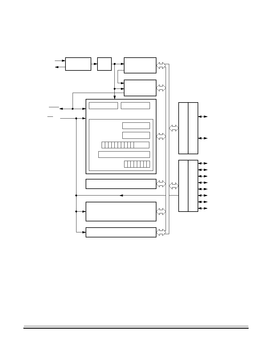
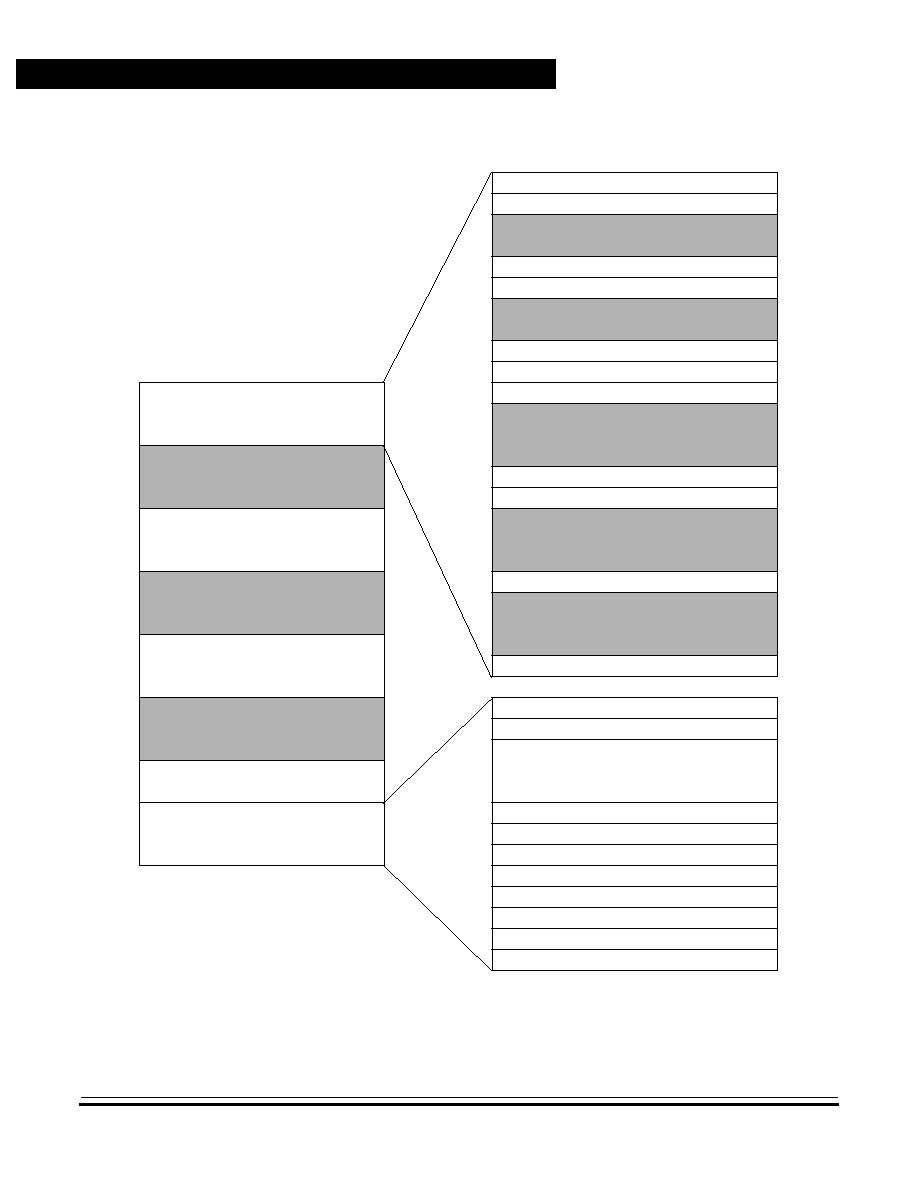
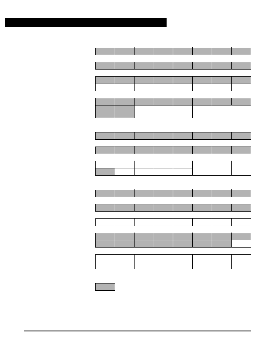
1.3 Structure
Figure 1-1. Block Diagram
0 0 0 0 0 0 0 0 1 1
WATCHDOG AND
ILLEGAL ADDRESS
DETECT
STATIC RAM (SRAM) ≠ 64 BYTES
ALU
CPU CONTROL
68HC05 CPU
ACCUMULATOR
INDEX REGISTER
STK PTR
PROGRAM COUNTER
CONDITION CODE
REGISTER
15-STAGE
MULTIFUNCTION
TIMER SYSTEM
DIVIDE
INTERNAL
OSCILLATOR
OSC1
OSC2
CPU REGISTERS
USER EPROM ≠ 1240 BYTES
MASK OPTION REGISTER (MOR)
10-mA sink capability on all I/O pins
DATA DIRECTION REGISTER A
DATA DIRECTION REGISTER B
PORT A
PORT B
PB3
(1)
PB2
(1)
PA7
PA6
PA5
PA4
PA3
(1) (2)
PA2
(1) (2)
PA1
(1) (2)
PA0
(1) (2)
RESET
IRQ/V
PP
1 1 1 H I N Z C
BY 2
Notes:
1. 5.5 mA source capability
2. External interrupt capability
Technical Data
MC68HC705KJ1 -- Rev. 2.0
22
Introduction
MOTOROLA
Introduction
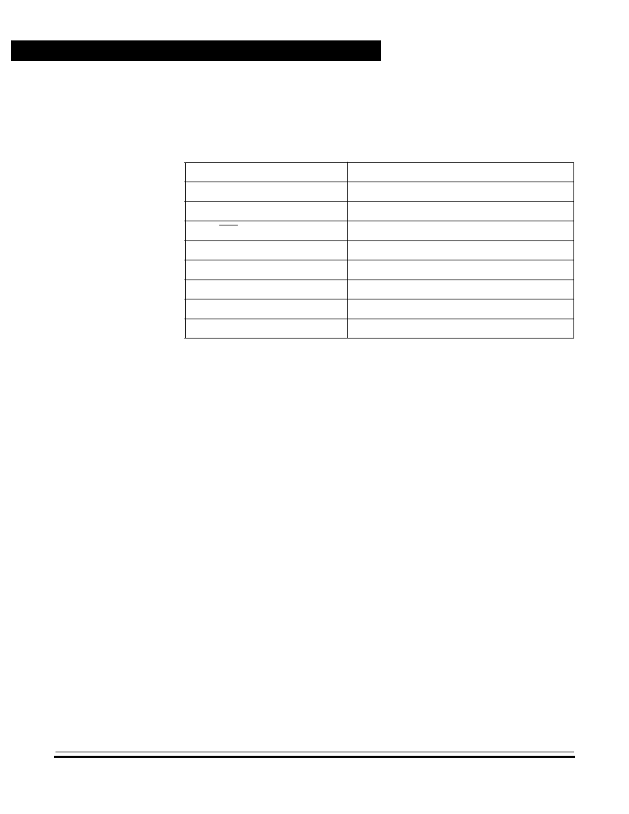
1.4 Programmable Options
The options in
Table 1-1
are programmable in the mask option register.
Table 1-1. Programmable Options
Feature
Option
COP Watchdog Timer
Enabled or Disabled
External Interrupt Triggering
Edge-Sensitive Only or Edge- and Level-Sensitive
Port A IRQ Pin Interrupts
Enabled or Disabled
Port Pulldown Resistors
Enabled or Disabled
STOP Instruction Mode
Stop Mode or Halt Mode
Crystal Oscillator Internal Resistor Enabled or Disabled
EPROM Security
Enabled or Disabled
Short Oscillator Delay Counter
Enabled or Disabled

MC68HC705KJ1 -- Rev. 2.0
Technical Data
MOTOROLA
Pin Descriptions
23
Technical Data -- MC68HC705KJ1
Section 2. Pin Descriptions
2.1 Contents
2.2
Pin Assignments . . . . . . . . . . . . . . . . . . . . . . . . . . . . . . . . . . . .24
2.3
Pin Functions . . . . . . . . . . . . . . . . . . . . . . . . . . . . . . . . . . . . . .24
2.3.1
V
DD
and V
SS
. . . . . . . . . . . . . . . . . . . . . . . . . . . . . . . . . . . . .24
2.3.2
OSC1 and OSC2 . . . . . . . . . . . . . . . . . . . . . . . . . . . . . . . . .25
2.3.2.1
Crystal Oscillator . . . . . . . . . . . . . . . . . . . . . . . . . . . . . . .25
2.3.2.2
Ceramic Resonator Oscillator . . . . . . . . . . . . . . . . . . . . .26
2.3.2.3
RC Oscillator . . . . . . . . . . . . . . . . . . . . . . . . . . . . . . . . . .28
2.3.2.4
External Clock . . . . . . . . . . . . . . . . . . . . . . . . . . . . . . . . .28
2.3.3
RESET . . . . . . . . . . . . . . . . . . . . . . . . . . . . . . . . . . . . . . . . .28
2.3.4
IRQ/V
PP
. . . . . . . . . . . . . . . . . . . . . . . . . . . . . . . . . . . . . . . .29
2.3.5
PA0≠PA7 . . . . . . . . . . . . . . . . . . . . . . . . . . . . . . . . . . . . . . .29
2.3.6
PB2 and PB3 . . . . . . . . . . . . . . . . . . . . . . . . . . . . . . . . . . . .29
Technical Data
MC68HC705KJ1 -- Rev. 2.0
24
Pin Descriptions
MOTOROLA
Pin Descriptions
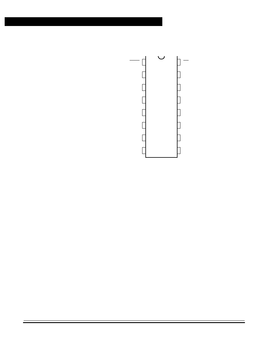
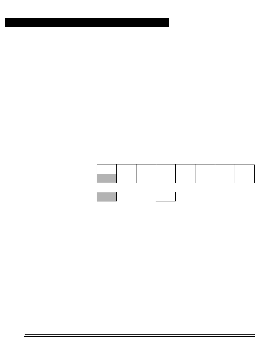
2.2 Pin Assignments
Figure 2-1. Pin Assignments
2.3 Pin Functions
The pin functions of the MCUs are described in these subsections.
2.3.1 V
DD
and V
SS
V
DD
and V
SS
are the power supply and ground pins. The MCU operates
from a single power supply.
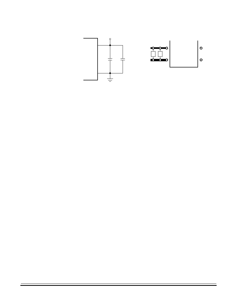
Very fast signal transitions occur on the MCU pins, placing high,
short-duration current demands on the power supply. To prevent noise
problems, take special care, as
Figure 2-2
shows, by placing the bypass
capacitors as close as possible to the MCU. C2 is an optional bulk
current bypass capacitor for use in applications that require the port pins
to source high current levels.
RESET
1
OSC1
2
OSC2
3
PB3
4
PB2
5
V
DD
6
V
SS
7
PA7
8
IRQ/V
PP
16
PA0
15
PA1
14
PA2
13
PA3
12
PA4
11
PA5
10
PA6
9
Pin Descriptions
Pin Functions
MC68HC705KJ1 -- Rev. 2.0
Technical Data
MOTOROLA
Pin Descriptions
25
Figure 2-2. Bypassing Layout Recommendation
2.3.2 OSC1 and OSC2
The OSC1 and OSC2 pins are the connections for the on-chip oscillator.
The oscillator can be driven by any of the following:
1. Standard crystal (See
Figure 2-3
and
Figure 2-4
.)
2. Ceramic resonator (See
Figure 2-5
and
Figure 2-6
.)
3. Resistor/capacitor (RC) oscillator (Refer to
Appendix A.
MC68HRC705KJ1
.)
4. External clock signal as shown in (See
Figure 2-7
.)
5. Low speed (32 kHz) crystal connections (Refer to
Appendix B.
MC68HLC705KJ1
.)
The frequency, f
OSC
, of the oscillator or external clock source is divided
by two to produce the internal operating frequency, f
OP
.
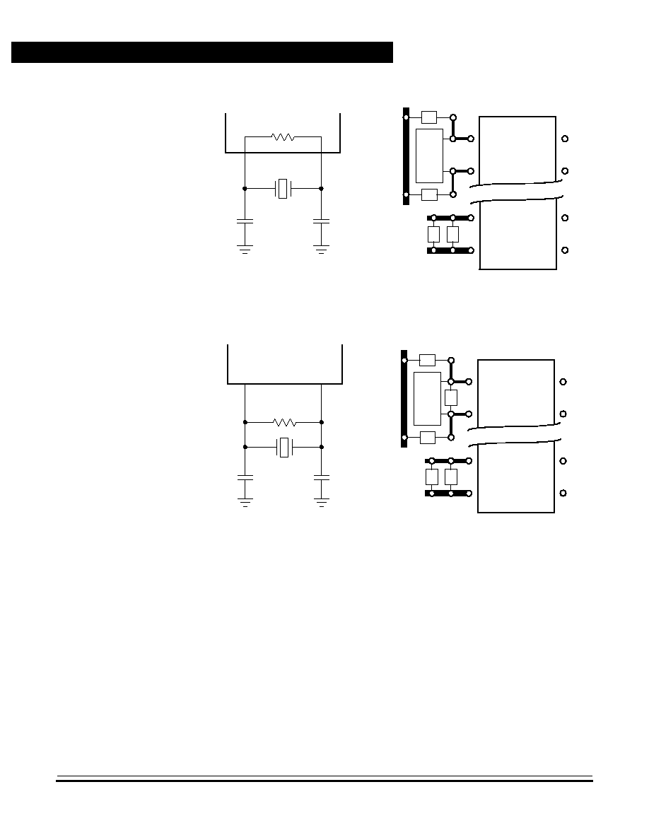
2.3.2.1 Crystal Oscillator
Figure 2-3
and
Figure 2-4
show a typical crystal oscillator circuit for an
AT-cut, parallel resonant crystal. Follow the crystal supplier's
recommendations, as the crystal parameters determine the external
component values required to provide reliable startup and maximum
stability. The load capacitance values used in the oscillator circuit design
should include all stray layout capacitances.
To minimize output distortion, mount the crystal and capacitors as close
as possible to the pins. An internal startup resistor of approximately
2 M
is provided between OSC1 and OSC2 for the crystal oscillator as
a programmable mask option.
NOTE:
Use an AT-cut crystal and not an AT-strip crystal because the MCU can
overdrive an AT-strip crystal.
C1
C2
MCU
C1
0.1
µ
F
C2
V+
+
V
DD
V
SS
V
DD
V
SS
Technical Data
MC68HC705KJ1 -- Rev. 2.0
26
Pin Descriptions
MOTOROLA
Pin Descriptions
Figure 2-3. Crystal Connections with
Oscillator Internal Resistor Mask Option
Figure 2-4. Crystal Connections without
Oscillator Internal Resistor Mask Option
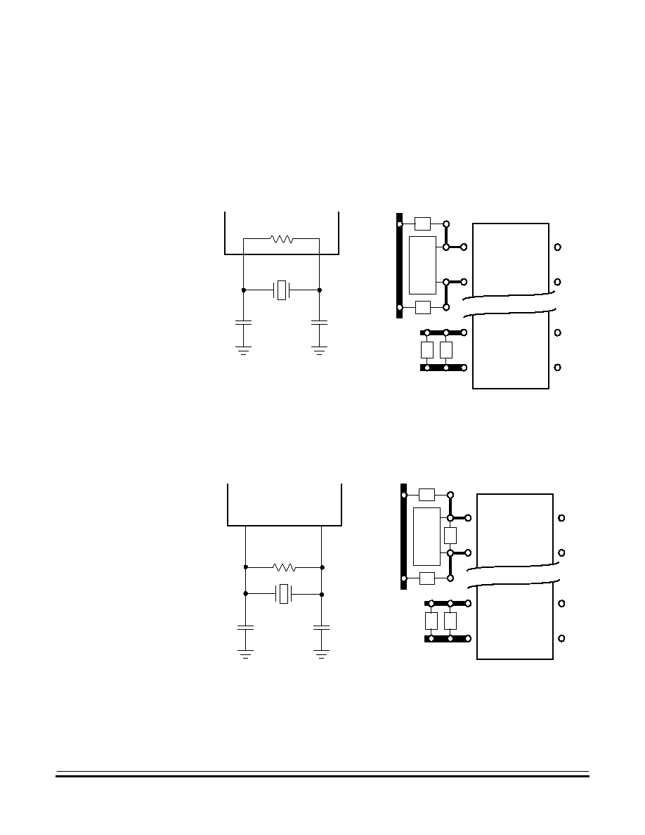
2.3.2.2 Ceramic Resonator Oscillator
To reduce cost, use a ceramic resonator instead of the crystal. The
circuits shown in
Figure 2-5
and
Figure 2-6
show ceramic resonator
circuits. Follow the resonator manufacturer's recommendations, as the
resonator parameters determine the external component values
required for maximum stability and reliable starting. The load
capacitance values used in the oscillator circuit design should include all
stray capacitances.
MCU
C1
C2
XTAL
C4
C3
XTAL
C3
27 pF
C4
27 pF
PA7
OSC2
PA7
OSC2
V
SS
V
DD
V
SS
MCU
C1
C2
R
XTAL
C4
C3
R
10 M
XTAL
C3
27 pF
C4
27 pF
PA7
OSC2
V
DD
V
SS
PA7
OSC2
V
SS
Pin Descriptions
Pin Functions
MC68HC705KJ1 -- Rev. 2.0
Technical Data
MOTOROLA
Pin Descriptions
27
Mount the resonator and components as close as possible to the pins for
startup stabilization and to minimize output distortion. An internal startup
resistor of approximately 2 M
is provided between OSC1 and OSC2 as
a programmable mask option.
Figure 2-5. Ceramic Resonator Connections with
Oscillator Internal Resistor Mask Option
Figure 2-6. Ceramic Resonator Connections without
Oscillator Internal Resistor Mask Option
MCU
C1
C2
CERAMIC
C4
C3
CERAMIC
C3
27 pF
C4
27 pF
RESONA
T
O
R
RESONATOR
PA7
OSC2
PA7
OSC2
V
DD
V
SS
V
SS
MCU
C1
C2
R
CERAMIC
C4
C3
R
10 M
CERAMIC
C3
27 pF
C4
27 pF
RESONA
T
O
R
RESONATOR
V
SS
V
DD
V
SS
PA7
OSC2
PA7
OSC2

Technical Data
MC68HC705KJ1 -- Rev. 2.0
28
Pin Descriptions
MOTOROLA
Pin Descriptions
2.3.2.3 RC Oscillator
Refer to
Appendix A. MC68HRC705KJ1
.
2.3.2.4 External Clock
An external clock from another CMOS-compatible device can be
connected to the OSC1 input, with the OSC2 input not connected, as
shown in
Figure 2-7
. This configuration is possible regardless of
whether the crystal/ceramic resonator or the RC oscillator is enabled.
Figure 2-7. External Clock Connections
2.3.3 RESET
Applying a logic 0 to the RESET pin forces the MCU to a known startup
state. An internal reset also pulls the RESET pin low. An internal resistor
to V
DD
pulls the RESET pin high. A steering diode between the RESET
and V
DD
pins discharges any RESET pin voltage when power is
removed from the MCU. The RESET pin contains an internal Schmitt
trigger to improve its noise immunity as an input. Refer to
Section 5.
Resets and Interrupts
for more information.
MCU
EXTERNAL
CMOS CLOCK
PA7
OSC2

Pin Descriptions
Pin Functions
MC68HC705KJ1 -- Rev. 2.0
Technical Data
MOTOROLA
Pin Descriptions
29
2.3.4 IRQ/V
PP
The external interrupt/programming voltage pin (IRQ/V
PP
) drives the
asynchronous IRQ interrupt function of the CPU. Additionally, it is used
to program the user EPROM and mask option register. (See
Section 3.
Memory
and
Section 9. External Interrupt Module (IRQ)
.)
The LEVEL bit in the mask option register provides negative
edge-sensitive triggering or both negative edge-sensitive and low
level-sensitive triggering for the interrupt function.
If level-sensitive triggering is selected, the IRQ/V
PP
input requires an
external resistor to V
DD
for wired-OR operation. If the IRQ/V
PP
pin is not
used, it must be tied to the V
DD
supply.
The IRQ/V
PP
pin contains an internal Schmitt trigger as part of its input
to improve noise immunity. The voltage on this pin should not exceed
V
DD
except when the pin is being used for programming the EPROM.
NOTE:
The mask option register can enable the PA0≠PA3 pins to function as
external interrupt pins.
2.3.5 PA0≠PA7
These eight input/output (I/O) lines comprise port A, a general-purpose
bidirectional I/O port. (See
Section 9. External Interrupt Module (IRQ)
for information on PA0≠PA3 external interrupts.)
2.3.6 PB2 and PB3
These two I/O lines comprise port B, a general-purpose bidirectional
I/O port.

Technical Data
MC68HC705KJ1 -- Rev. 2.0
30
Pin Descriptions
MOTOROLA
Pin Descriptions

MC68HC705KJ1 -- Rev. 2.0
Technical Data
MOTOROLA
Memory
31
Technical Data -- MC68HC705KJ1
Section 3. Memory
3.1 Contents
3.2
Features . . . . . . . . . . . . . . . . . . . . . . . . . . . . . . . . . . . . . . . . . .31
3.3
Memory Map. . . . . . . . . . . . . . . . . . . . . . . . . . . . . . . . . . . . . . .32
3.4
Input/Output Register Summary . . . . . . . . . . . . . . . . . . . . . . .33
3.5
RAM . . . . . . . . . . . . . . . . . . . . . . . . . . . . . . . . . . . . . . . . . . . . .35
3.6
EPROM/OTPROM . . . . . . . . . . . . . . . . . . . . . . . . . . . . . . . . . .35
3.6.1
EPROM/OTPROM Programming . . . . . . . . . . . . . . . . . . . . .36
3.6.2
EPROM Programming Register . . . . . . . . . . . . . . . . . . . . .36
3.6.3
EPROM Erasing . . . . . . . . . . . . . . . . . . . . . . . . . . . . . . . . . .37
3.7
Mask Option Register . . . . . . . . . . . . . . . . . . . . . . . . . . . . . . . .38
3.8
EPROM Programming Characteristics . . . . . . . . . . . . . . . . . . .40
3.2 Features
Memory features include:
∑
1232 Bytes of User EPROM, Plus Eight Bytes for User Vectors
∑
64 Bytes of User RAM
Technical Data
MC68HC705KJ1 -- Rev. 2.0
32
Memory
MOTOROLA
Memory
3.3 Memory Map
Port A Data Register (PORTA)
$0000
Port B Data Register (PORTB)
$0001
Unimplemented
$0002
$0003
Data Direction Register A (DDRA)
$0004
Data Direction Register B (DDRB)
$0005
Unimplemented
$0006
$0007
Timer Status and Control Register (TSCR)
$0008
Timer Control Register (TCR)
$0009
$0000
I/O Registers
32 Bytes
IRQ Status and Control Register (ISCR)
$000A
Unimplemented
$000B
$001F
$0020
Unimplemented
160 Bytes
$000F
Pulldown Register Port A (PDRA)
$0010
$00BF
Pulldown Register Port B (PDRB)
$0011
$00C0
RAM
64 Bytes
Unimplemented
$0012
$00FF
$0017
$0100
Unimplemented
512 Bytes
EPROM Programming Register (EPROG)
$0018
Unimplemented
$0019
$02FF
$0300
EPROM
1232 Bytes
$001E
Reserved
$001F
$07CF
$07D0
Unimplemented
30 Bytes
COP Register (COPR)
(1)
$07F0
Mask Option Register (MOR)
$07F1
$07ED
Reserved
$07F2
$07EE
Test ROM
2 Bytes
$07EF
$07F7
$07F0
Registers and EPROM
16 Bytes
Timer Interrupt Vector High
$07F8
Timer Interrupt Vector Low
$07F9
$07FF
External Interrupt Vector High
$07FA
External Interrupt Vector Low
$07FB
Software Interrupt Vector High
$07FC
Software Interrupt Vector Low
$07FD
Reset Vector High
$07FE
Reset Vector Low
$07FF
(1)
Writing to bit 0 of $07F0 clears the COP watchdog.
Figure 3-1. Memory Map
Memory
Input/Output Register Summary
MC68HC705KJ1 -- Rev. 2.0
Technical Data
MOTOROLA
Memory
33
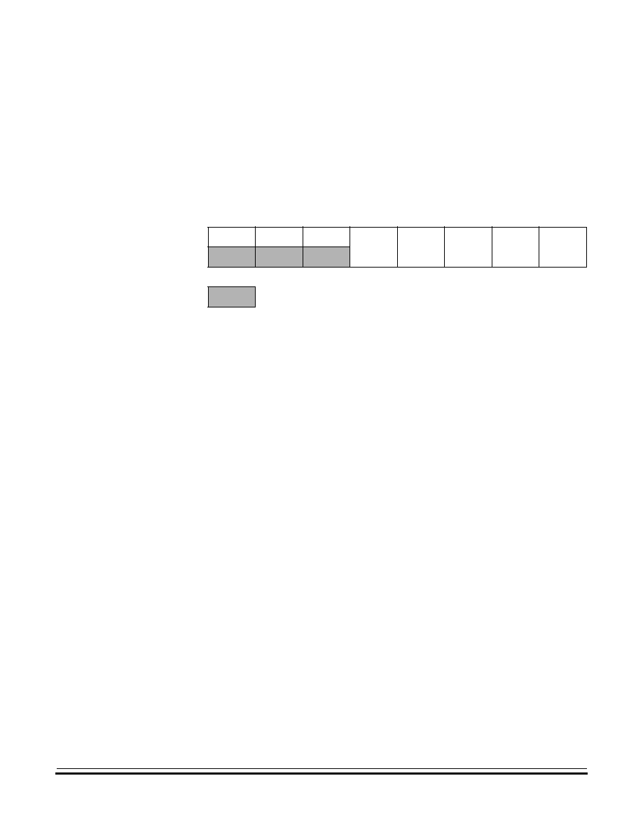
3.4 Input/Output Register Summary
Addr.
Register Name
Bit 7
6
5
4
3
2
1
Bit 0
$0000
Port A Data Register
(PORTA)
See page 83.
Read:
PA7
PA6
PA5
PA4
PA3
PA2
PA1
PA0
Write:
Reset:
Unaffected by Reset
$0001
Port B Data Register
(PORTB)
See page 86.
Read:
0
0
Refer to
Section 7.
Parallel I/O Ports
PB3
PB2
Refer to
Section 7.
Parallel I/O Ports
Write:
Reset:
Unaffected by Reset
$0002
Unimplemented
$0003
Unimplemented
$0004
Data Direction Register A
(DDRA)
See page 83.
Read:
DDRA7
DDRA6
DDRA5
DDRA4
DDRA3
DDRA2
DDRA1
DDRA0
Write:
Reset:
0
0
0
0
0
0
0
0
$0005
Data Direction Register B
(DDRB)
See page 87.
Read:
0
0
Refer to
Section 7.
Parallel I/O Ports
DDRB3
DDRB2
Refer to
Section 7.
Parallel I/O Ports
Write:
Reset:
0
0
0
0
0
0
0
0
$0006
Unimplemented
$0007
Unimplemented
$0008
Timer Status and Control
Register (TSCR)
See page 108.
Read:
TOF
RTIF
TOIE
RTIE
0
0
RT1
RT0
Write:
TOFR
RTIFR
Reset:
0
0
0
0
0
0
1
1
$0009
Timer Counter Register
(TCR)
See page 110.
Read:
TCR7
TCR6
TCR5
TCR4
TCR3
TCR2
TCR1
TCR0
Write:
Reset:
0
0
0
0
0
0
0
0
$000A
IRQ Status and Control
Register (ISCR)
See page 102.
Read:
IRQE
0
0
0
IRQF
0
0
0
Write:
R
IRQR
Reset:
1
0
0
0
0
0
0
0
= Unimplemented
R = Reserved
U = Unaffected
Figure 3-2. I/O Register Summary (Sheet 1 of 2)
Technical Data
MC68HC705KJ1 -- Rev. 2.0
34
Memory
MOTOROLA
Memory
$000B
Unimplemented
$000F
Unimplemented
$0010
Pulldown Register Port A
(PDRA)
See page 85.
Read:
Write:
PDIA7
PDIA6
PDIA5
PDIA4
PDIA3
PDIA2
PDIA1
PDIA0
Reset:
0
0
0
0
0
0
0
0
$0011
Pulldown Register Port B
(PDRB)
See page 89.
Read:
Write:
Refer to
Section 7.
Parallel I/O Ports
PDIB3
PDIB2
Refer to
Section 7.
Parallel I/O Ports
Reset:
0
0
0
0
0
0
0
0
$0012
Unimplemented
$0017
Unimplemented
$0018
EPROM Programming
Register (EPROG)
See page 36.
Read:
0
0
0
0
0
ELAT
MPGM
EPGM
Write:
R
R
R
R
Reset:
0
0
0
0
0
0
0
0
$0019
Unimplemented
$001E
Unimplemented
$001F
Reserved
R
R
R
R
R
R
R
R
$07F0
COP Register (COPR)
See page 95.
Read:
Write:
COPC
Reset:
U
U
U
U
U
U
U
0
$07F1
Mask Option Register
(MOR)
See page 38.
Read:
SOSCD
EPMSEC OSCRES
SWAIT
PDI
PIRQ
LEVEL
COPEN
Write:
Reset:
Unaffected by reset
Addr.
Register Name
Bit 7
6
5
4
3
2
1
Bit 0
= Unimplemented
R = Reserved
U = Unaffected
Figure 3-2. I/O Register Summary (Sheet 2 of 2)

Memory
RAM
MC68HC705KJ1 -- Rev. 2.0
Technical Data
MOTOROLA
Memory
35
3.5 RAM
The 64 addresses from $00C0 to $00FF serve as both the user RAM
and the stack RAM. Before processing an interrupt, the CPU uses five
bytes of the stack to save the contents of the CPU registers. During a
subroutine call, the CPU uses two bytes of the stack to store the return
address. The stack pointer decrements when the CPU stores a byte on
the stack and increments when the CPU retrieves a byte from the stack.
NOTE:
Be careful when using nested subroutines or multiple interrupt levels.
The CPU may overwrite data in the RAM during a subroutine or during
the interrupt stacking operation.
3.6 EPROM/OTPROM
An MCU with a quartz window has 1240 bytes of erasable,
programmable ROM (EPROM). The quartz window allows EPROM
erasure with ultraviolet light.
NOTE:
Keep the quartz window covered with an opaque material except when
erasing the MCU. Ambient light can affect MCU operation.
In an MCU without the quartz window, the EPROM cannot be erased
and serves as 1240 bytes of one-time programmable ROM (OTPROM).
The following addresses are user EPROM/OTPROM locations:
∑
$0300≠$07CF
∑
$07F8≠$07FF, used for user-defined interrupt and reset vectors
The COP register (COPR) is an EPROM/OTPROM location at address
$07F0.
The mask option register (MOR) is an EPROM/OTPROM location at
address $07F1.
Technical Data
MC68HC705KJ1 -- Rev. 2.0
36
Memory
MOTOROLA
Memory
3.6.1 EPROM/OTPROM Programming
The two ways to program the EPROM/OTPROM are:
∑
Manipulating the control bits in the EPROM programming register
to program the EPROM/OTPROM on a byte-by-byte basis
∑
Programming the EPROM/OTPROM with the M68HC705J
In-Circuit Simulator (M68HC705JICS) available from Motorola
3.6.2 EPROM Programming Register
The EPROM programming register (EPROG) contains the control bits
for programming the EPROM/OTPROM.
ELAT -- EPROM Bus Latch Bit
This read/write bit latches the address and data buses for
EPROM/OTPROM programming. Clearing the ELAT bit automatically
clears the EPGM bit. EPROM/OTPROM data cannot be read while
the ELAT bit is set. Reset clears the ELAT bit.
1 = Address and data buses configured for EPROM/OTPROM
programming the EPROM
0 = Address and data buses configured for normal operation
MPGM -- MOR Programming Bit
This read/write bit applies programming power from the IRQ/V
PP
pin
to the mask option register. Reset clears MPGM.
1 = Programming voltage applied to MOR
0 = Programming voltage not applied to MOR
Address:
$0018
Bit 7
6
5
4
3
2
1
Bit 0
Read:
0
0
0
0
0
ELAT
MPGM
EPGM
Write:
R
R
R
R
Reset:
0
0
0
0
0
0
0
0
= Unimplemented
R
= Reserved
Figure 3-3. EPROM Programming Register (EPROG)

Memory
EPROM/OTPROM
MC68HC705KJ1 -- Rev. 2.0
Technical Data
MOTOROLA
Memory
37
EPGM -- EPROM Programming Bit
This read/write bit applies the voltage from the IRQ/V
PP
pin to the
EPROM. To write the EPGM bit, the ELAT bit must be set already.
Reset clears EPGM.
1 = Programming voltage (IRQ/V
PP
pin) applied to EPROM
0 = Programming voltage (IRQ/V
PP
pin) not applied to EPROM
NOTE:
Writing logic 1s to both the ELAT and EPGM bits with a single instruction
sets ELAT and clears EPGM. ELAT must be set first by a separate
instruction.
Bits [7:3] -- Reserved
Take the following steps to program a byte of EPROM/OTPROM:
1. Apply the programming voltage, V
PP
, to the IRQ/V
PP
pin.
2. Set the ELAT bit.
3. Write to any EPROM/OTPROM address.
4. Set the EPGM bit and wait for a time, t
EPGM
.
5. Clear the ELAT bit.
3.6.3 EPROM Erasing
The erased state of an EPROM bit is logic 0. Erase the EPROM by
exposing it to 15 Ws/cm
2
of ultraviolet light with a wavelength of 2537
angstroms. Position the ultraviolet light source one inch from the
EPROM. Do not use a shortwave filter.

Technical Data
MC68HC705KJ1 -- Rev. 2.0
38
Memory
MOTOROLA
Memory
3.7 Mask Option Register
The mask option register (MOR) is an EPROM/OTPROM byte that
controls the following options:
∑
COP watchdog (enable or disable)
∑
External interrupt pin triggering (edge-sensitive only or edge- and
level-sensitive)
∑
Port A external interrupts (enable or disable)
∑
Port pulldown resistors (enable or disable)
∑
STOP instruction (stop mode or halt mode)
∑
Crystal oscillator internal resistor (enable or disable)
∑
EPROM security (enable or disable)
∑
Short oscillator delay (enable or disable)
Take the following steps to program the mask option register (MOR):
1. Apply the programming voltage, V
PP
, to the IRQ/V
PP
pin.
2. Write to the MOR.
3. Set the MPGM bit and wait for a time, t
MPGM
.
4. Clear the MPGM bit.
5. Reset the MCU.
Address:
$07F1
Bit 7
6
5
4
3
2
1
Bit 0
Read:
SOSCD
EPMSEC OSCRES
SWAIT
SWPDI
PIRQ
LEVEL
COPEN
Write:
Reset:
Unaffected by reset
Figure 3-4. Mask Option Register (MOR)

Memory
Mask Option Register
MC68HC705KJ1 -- Rev. 2.0
Technical Data
MOTOROLA
Memory
39
SOSCD -- Short Oscillator Delay Bit
The SOSCD bit controls the oscillator stabilization counter. The
normal stabilization delay following reset or exit from stop mode is
4064 t
cyc
. Setting SOSCD enables a 128 t
cyc
stabilization delay.
1 = Short oscillator delay enabled
0 = Short oscillator delay disabled
EPMSEC -- EPROM Security Bit
The EPMSEC bit controls access to the EPROM/OTPROM.
1 = External access to EPROM/OTPROM denied
0 = External access to EPROM/OTPROM not denied
OSCRES -- Oscillator Internal Resistor Bit
The OSCRES bit enables a 2-M
internal resistor in the oscillator
circuit.
1 = Oscillator internal resistor enabled
0 = Oscillator internal resistor disabled
NOTE:
Program the OSCRES bit to logic 0 in devices using low-speed crystal
or RC oscillators with external resistor.
SWAIT -- Stop-to-Wait Conversion Bit
The SWAIT bit enables halt mode. When the SWAIT bit is set, the
CPU interprets the STOP instruction as a WAIT instruction, and the
MCU enters halt mode. Halt mode is the same as wait mode, except
that an oscillator stabilization delay of 1 to 4064 t
cyc
occurs after
exiting halt mode.
1 = Halt mode enabled
0 = Halt mode not enabled
SWPDI -- Software Pulldown Inhibit Bit
The SWPDI bit inhibits software control of the I/O port pulldown
devices. The SWPDI bit overrides the pulldown inhibit bits in the port
pulldown inhibit registers.
1 = Software pulldown control inhibited
0 = Software pulldown control not inhibited
Technical Data
MC68HC705KJ1 -- Rev. 2.0
40
Memory
MOTOROLA
Memory
PIRQ -- Port A External Interrupt Bit
The PIRQ bit enables the PA0≠PA3 pins to function as external
interrupt pins.
1 = PA0≠PA3 enabled as external interrupt pins
0 = PA0≠PA3 not enabled as external interrupt pins
LEVEL --External Interrupt Sensitivity Bit
The LEVEL bit controls external interrupt triggering sensitivity.
1 = External interrupts triggered by active edges and active levels
0 = External interrupts triggered only by active edges
COPEN -- COP Enable Bit
The COPEN bit enables the COP watchdog.
1 = COP watchdog enabled
0 = COP watchdog disabled
3.8 EPROM Programming Characteristics
Table 3-1. EPROM Programming Characteristics
(1)
1. V
DD
= 5.0 Vdc
±
10%, V
SS
= 0 Vdc, T
A
= ≠40
∞
C to +85
∞
C
Characteristic
Symbol
Min
Typ
Max
Unit
Programming Voltage
IRQ/V
PP
V
PP
16.0
16.5
17.0
V
Programming Current
IRQ/V
PP
I
PP
--
3.0
10.0
mA
Programming Time
Per Array Byte
MOR
t
EPGM
t
MPGM
4
4
--
--
--
--
ms

MC68HC705KJ1 -- Rev. 2.0
Technical Data
MOTOROLA
Central Processor Unit (CPU)
41
Technical Data -- MC68HC705KJ1
Section 4. Central Processor Unit (CPU)
4.1 Contents
4.2
Introduction . . . . . . . . . . . . . . . . . . . . . . . . . . . . . . . . . . . . . . . .42
4.3
Features . . . . . . . . . . . . . . . . . . . . . . . . . . . . . . . . . . . . . . . . . .42
4.4
CPU Control Unit . . . . . . . . . . . . . . . . . . . . . . . . . . . . . . . . . . .43
4.5
Arithmetic/Logic Unit. . . . . . . . . . . . . . . . . . . . . . . . . . . . . . . . .43
4.6
CPU Registers . . . . . . . . . . . . . . . . . . . . . . . . . . . . . . . . . . . . .44
4.6.1
Accumulator . . . . . . . . . . . . . . . . . . . . . . . . . . . . . . . . . . . . .44
4.6.2
Index Register . . . . . . . . . . . . . . . . . . . . . . . . . . . . . . . . . . .44
4.6.3
Stack Pointer . . . . . . . . . . . . . . . . . . . . . . . . . . . . . . . . . . . .45
4.6.4
Program Counter . . . . . . . . . . . . . . . . . . . . . . . . . . . . . . . . .46
4.6.5
Condition Code Register . . . . . . . . . . . . . . . . . . . . . . . . . . .47
4.7
Instruction Set. . . . . . . . . . . . . . . . . . . . . . . . . . . . . . . . . . . . . .48
4.7.1
Addressing Modes . . . . . . . . . . . . . . . . . . . . . . . . . . . . . . . .48
4.7.1.1
Inherent . . . . . . . . . . . . . . . . . . . . . . . . . . . . . . . . . . . . . .49
4.7.1.2
Immediate . . . . . . . . . . . . . . . . . . . . . . . . . . . . . . . . . . . .49
4.7.1.3
Direct . . . . . . . . . . . . . . . . . . . . . . . . . . . . . . . . . . . . . . . .49
4.7.1.4
Extended . . . . . . . . . . . . . . . . . . . . . . . . . . . . . . . . . . . . .49
4.7.1.5
Indexed, No Offset . . . . . . . . . . . . . . . . . . . . . . . . . . . . . .49
4.7.1.6
Indexed, 8-Bit Offset . . . . . . . . . . . . . . . . . . . . . . . . . . . .50
4.7.1.7
Indexed, 16-Bit Offset . . . . . . . . . . . . . . . . . . . . . . . . . . .50
4.7.1.8
Relative . . . . . . . . . . . . . . . . . . . . . . . . . . . . . . . . . . . . . .50
4.7.2
Instruction Types . . . . . . . . . . . . . . . . . . . . . . . . . . . . . . . . .51
4.7.2.1
Register/Memory Instructions . . . . . . . . . . . . . . . . . . . . .51
4.7.2.2
Read-Modify-Write Instructions . . . . . . . . . . . . . . . . . . . .52
4.7.2.3
Jump/Branch Instructions. . . . . . . . . . . . . . . . . . . . . . . . .53
4.7.2.4
Bit Manipulation Instructions . . . . . . . . . . . . . . . . . . . . . .55
4.7.2.5
Control Instructions . . . . . . . . . . . . . . . . . . . . . . . . . . . . .55
4.7.3
Instruction Set Summary . . . . . . . . . . . . . . . . . . . . . . . . . . .56

Technical Data
MC68HC705KJ1 -- Rev. 2.0
42
Central Processor Unit (CPU)
MOTOROLA
Central Processor Unit (CPU)
4.2 Introduction
The central processor unit (CPU) consists of a CPU control unit, an
arithmetic/logic unit (ALU), and five CPU registers. The CPU control unit
fetches and decodes instructions. The ALU executes the instructions.
The CPU registers contain data, addresses, and status bits that reflect
the results of CPU operations.
4.3 Features
Features of the CPU include:
∑
4.0-MHz Bus Frequency on Standard Part
∑
8-Bit Accumulator
∑
8-Bit Index Register
∑
11-Bit Program Counter
∑
6-Bit Stack Pointer
∑
Condition Code Register with Five Status Flags
∑
62 Instructions
∑
8 Addressing Modes
∑
Power-Saving Stop, Wait, Halt, and Data-Retention Modes
Central Processor Unit (CPU)
CPU Control Unit
MC68HC705KJ1 -- Rev. 2.0
Technical Data
MOTOROLA
Central Processor Unit (CPU)
43
Figure 4-1. Programming Model
4.4 CPU Control Unit
The CPU control unit fetches and decodes instructions during program
operation. The control unit selects the memory locations to read and
write and coordinates the timing of all CPU operations.
4.5 Arithmetic/Logic Unit
The arithmetic/logic unit (ALU) performs the arithmetic, logic, and
manipulation operations decoded from the instruction set by the CPU
control unit. The ALU produces the results called for by the program and
sets or clears status and control bits in the condition code register
(CCR).
ACCUMULATOR (A)
INDEX REGISTER (X)
CONDITION CODE REGISTER (CCR)
PROGRAM COUNTER (PC)
STACK POINTER (SP)
HALF-CARRY FLAG
INTERRUPT MASK
NEGATIVE FLAG
ZERO FLAG
CARRY/BORROW FLAG
0
4
7
5
6
3
2
1
0
ARITHMETIC/LOGIC UNIT
CPU CONTROL UNIT
0
4
7
5
6
3
2
1
0
4
7
5
6
3
2
1
8
12
15
13
14
11 10
9
0
0
0
0
0
0
0
1
1
0
0
0
0
4
7
5
6
3
2
1
8
12
15
13
14
11 10
9
1
1
1
H
I
N
Z
C
0
4
7
5
6
3
2
1
0
0

Technical Data
MC68HC705KJ1 -- Rev. 2.0
44
Central Processor Unit (CPU)
MOTOROLA
Central Processor Unit (CPU)
4.6 CPU Registers
The M68HC05 CPU contains five registers that control and monitor MCU
operation:
∑
Accumulator
∑
Index register
∑
Stack pointer
∑
Program counter
∑
Condition code register
CPU registers are not memory mapped.
4.6.1 Accumulator
The accumulator is a general-purpose 8-bit register. The CPU uses the
accumulator to hold operands and results of ALU operations.
4.6.2 Index Register
In the indexed addressing modes, the CPU uses the byte in the index
register to determine the conditional address of the operand. The index
register also can serve as a temporary storage location or a counter.
Bit 7
6
5
4
3
2
1
Bit 0
Read:
Write:
Reset:
Unaffected by reset
Figure 4-2. Accumulator (A)
Bit 7
6
5
4
3
2
1
Bit 0
Read:
Write:
Reset:
Unaffected by reset
Figure 4-3. Index Register (X)

Central Processor Unit (CPU)
CPU Registers
MC68HC705KJ1 -- Rev. 2.0
Technical Data
MOTOROLA
Central Processor Unit (CPU)
45
4.6.3 Stack Pointer
The stack pointer is a 16-bit register that contains the address of the next
location on the stack. During a reset or after the reset stack pointer
instruction (RSP), the stack pointer is preset to $00FF. The address in
the stack pointer decrements after a byte is stacked and increments
before a byte is unstacked.
The 10 most significant bits of the stack pointer are permanently fixed at
0000000011, so the stack pointer produces addresses from $00C0 to
$00FF. If subroutines and interrupts use more than 64 stack locations,
the stack pointer wraps around to address $00FF and begins writing
over the previously stored data. A subroutine uses two stack locations;
an interrupt uses five locations.
Bit
15
14
13
12
11
10
9
8
7
6
5
4
3
2
1
Bit
0
Read:
0
0
0
0
0
0
0
0
1
1
Write:
Reset:
0
0
0
0
0
0
0
0
1
1
1
1
1
1
1
1
= Unimplemented
Figure 4-4. Stack Pointer (SP)

Technical Data
MC68HC705KJ1 -- Rev. 2.0
46
Central Processor Unit (CPU)
MOTOROLA
Central Processor Unit (CPU)
4.6.4 Program Counter
The program counter is a 16-bit register that contains the address of the
next instruction or operand to be fetched. The five most significant bits
of the program counter are ignored and appear as 00000.
Normally, the address in the program counter automatically increments
to the next sequential memory location every time an instruction or
operand is fetched. Jump, branch, and interrupt operations load the
program counter with an address other than that of the next sequential
location.
Bit
15
14
13
12
11
10
9
8
7
6
5
4
3
2
1
Bit
0
Reset:
0
0
0
0
0
Loaded with vector from $07FE and $07FF
Figure 4-5. Program Counter (PC)
Central Processor Unit (CPU)
CPU Registers
MC68HC705KJ1 -- Rev. 2.0
Technical Data
MOTOROLA
Central Processor Unit (CPU)
47
4.6.5 Condition Code Register
The condition code register is an 8-bit register whose three most
significant bits are permanently fixed at 111. The condition code register
contains the interrupt mask and four flags that indicate the results of the
instruction just executed.
H -- Half-Carry Flag
The CPU sets the half-carry flag when a carry occurs between bits 3
and 4 of the accumulator during an ADD or ADC operation. The
half-carry flag is required for binary-coded decimal (BCD) arithmetic
operations.
I -- Interrupt Mask
Setting the interrupt mask disables interrupts. If an interrupt request
occurs while the interrupt mask is logic 0, the CPU saves the CPU
registers on the stack, sets the interrupt mask, and then fetches the
interrupt vector. If an interrupt request occurs while the interrupt mask
is logic 1, the interrupt request is latched. Normally, the CPU
processes the latched interrupt request as soon as the interrupt mask
is cleared again.
A return from interrupt instruction (RTI) unstacks the CPU registers,
restoring the interrupt mask to its cleared state. After any reset, the
interrupt mask is set and can be cleared only by a software
instruction.
N -- Negative Flag
The CPU sets the negative flag when an ALU operation produces a
negative result.
Bit 7
6
5
4
3
2
1
Bit 0
Read:
1
1
1
H
I
N
Z
C
Write:
Reset:
1
1
1
U
1
U
U
U
= Unimplemented
U = Unaffected
Figure 4-6. Condition Code Register (CCR)

Technical Data
MC68HC705KJ1 -- Rev. 2.0
48
Central Processor Unit (CPU)
MOTOROLA
Central Processor Unit (CPU)
Z -- Zero Flag
The CPU sets the zero flag when an ALU operation produces a result
of $00.
C -- Carry/Borrow Flag
The CPU sets the carry/borrow flag when an addition operation
produces a carry out of bit 7 of the accumulator or when a subtraction
operation requires a borrow. Some logical operations and data
manipulation instructions also clear or set the carry/borrow flag.
4.7 Instruction Set
The MCU instruction set has 62 instructions and uses eight addressing
modes.
4.7.1 Addressing Modes
The CPU uses eight addressing modes for flexibility in accessing data.
The addressing modes provide eight different ways for the CPU to find
the data required to execute an instruction. The eight addressing
modes are:
∑
Inherent
∑
Immediate
∑
Direct
∑
Extended
∑
Indexed, no offset
∑
Indexed, 8-bit offset
∑
Indexed, 16-bit offset
∑
Relative

Central Processor Unit (CPU)
Instruction Set
MC68HC705KJ1 -- Rev. 2.0
Technical Data
MOTOROLA
Central Processor Unit (CPU)
49
4.7.1.1 Inherent
Inherent instructions are those that have no operand, such as
return-from-interrupt (RTI) and stop (STOP). Some of the inherent
instructions act on data in the CPU registers, such as set carry flag
(SEC) and increment accumulator (INCA). Inherent instructions require
no operand address and are one byte long.
4.7.1.2 Immediate
Immediate instructions are those that contain a value to be used in an
operation with the value in the accumulator or index register. Immediate
instructions require no operand address and are two bytes long. The
opcode is the first byte, and the immediate data value is the second byte.
4.7.1.3 Direct
Direct instructions can access any of the first 256 memory locations with
two bytes. The first byte is the opcode, and the second is the low byte of
the operand address. In direct addressing, the CPU automatically uses
$00 as the high byte of the operand address.
4.7.1.4 Extended
Extended instructions use three bytes and can access any address in
memory. The first byte is the opcode; the second and third bytes are the
high and low bytes of the operand address.
When using the Motorola assembler, the programmer does not need to
specify whether an instruction is direct or extended. The assembler
automatically selects the shortest form of the instruction.
4.7.1.5 Indexed, No Offset
Indexed instructions with no offset are 1-byte instructions that can
access data with variable addresses within the first 256 memory
locations. The index register contains the low byte of the effective
address of the operand. The CPU automatically uses $00 as the high
byte, so these instructions can address locations $0000≠$00FF.
Indexed, no offset instructions are often used to move a pointer through
a table or to hold the address of a frequently used RAM or input/output
(I/O) location.

Technical Data
MC68HC705KJ1 -- Rev. 2.0
50
Central Processor Unit (CPU)
MOTOROLA
Central Processor Unit (CPU)
4.7.1.6 Indexed, 8-Bit Offset
Indexed, 8-bit offset instructions are 2-byte instructions that can access
data with variable addresses within the first 511 memory locations. The
CPU adds the unsigned byte in the index register to the unsigned byte
following the opcode. The sum is the effective address of the operand.
These instructions can access locations $0000≠$01FE.
Indexed 8-bit offset instructions are useful for selecting the kth element
in an n-element table. The table can begin anywhere within the first 256
memory locations and could extend as far as location 510 ($01FE). The
k value is typically in the index register, and the address of the beginning
of the table is in the byte following the opcode.
4.7.1.7 Indexed, 16-Bit Offset
Indexed, 16-bit offset instructions are 3-byte instructions that can access
data with variable addresses at any location in memory. The CPU adds
the unsigned byte in the index register to the two unsigned bytes
following the opcode. The sum is the effective address of the operand.
The first byte after the opcode is the high byte of the 16-bit offset; the
second byte is the low byte of the offset.
Indexed, 16-bit offset instructions are useful for selecting the kth element
in an n-element table anywhere in memory.
As with direct and extended addressing, the Motorola assembler
determines the shortest form of indexed addressing.
4.7.1.8 Relative
Relative addressing is only for branch instructions. If the branch
condition is true, the CPU finds the effective branch destination by
adding the signed byte following the opcode to the contents of the
program counter. If the branch condition is not true, the CPU goes to the
next instruction. The offset is a signed, two's complement byte that gives
a branching range of ≠128 to +127 bytes from the address of the next
location after the branch instruction.
When using the Motorola assembler, the programmer does not need to
calculate the offset because the assembler determines the proper offset
and verifies that it is within the span of the branch.

Central Processor Unit (CPU)
Instruction Set
MC68HC705KJ1 -- Rev. 2.0
Technical Data
MOTOROLA
Central Processor Unit (CPU)
51
4.7.2 Instruction Types
The MCU instructions fall into the following five categories:
∑
Register/memory instructions
∑
Read-modify-write instructions
∑
Jump/branch instructions
∑
Bit manipulation instructions
∑
Control instructions
4.7.2.1 Register/Memory Instructions
These instructions operate on CPU registers and memory locations.
Most of them use two operands. One operand is in either the
accumulator or the index register. The CPU finds the other operand in
memory.
Table 4-1. Register/Memory Instructions
Instruction
Mnemonic
Add Memory Byte and Carry Bit to Accumulator
ADC
Add Memory Byte to Accumulator
ADD
AND Memory Byte with Accumulator
AND
Bit Test Accumulator
BIT
Compare Accumulator
CMP
Compare Index Register with Memory Byte
CPX
EXCLUSIVE OR Accumulator with Memory Byte
EOR
Load Accumulator with Memory Byte
LDA
Load Index Register with Memory Byte
LDX
Multiply
MUL
OR Accumulator with Memory Byte
ORA
Subtract Memory Byte and Carry Bit from Accumulator
SBC
Store Accumulator in Memory
STA
Store Index Register in Memory
STX
Subtract Memory Byte from Accumulator
SUB
Technical Data
MC68HC705KJ1 -- Rev. 2.0
52
Central Processor Unit (CPU)
MOTOROLA
Central Processor Unit (CPU)
4.7.2.2 Read-Modify-Write Instructions
These instructions read a memory location or a register, modify its
contents, and write the modified value back to the memory location or to
the register.
NOTE:
Do not use read-modify-write instructions on registers with
write-only bits.
Table 4-2. Read-Modify-Write Instructions
Instruction
Mnemonic
Arithmetic Shift Left (Same as LSL)
ASL
Arithmetic Shift Right
ASR
Bit Clear
BCLR
(1)
1. Unlike other read-modify-write instructions, BCLR and
BSET use only direct addressing.
Bit Set
BSET
(1)
Clear Register
CLR
Complement (One's Complement)
COM
Decrement
DEC
Increment
INC
Logical Shift Left (Same as ASL)
LSL
Logical Shift Right
LSR
Negate (Two's Complement)
NEG
Rotate Left through Carry Bit
ROL
Rotate Right through Carry Bit
ROR
Test for Negative or Zero
TST
(2)
2. TST is an exception to the read-modify-write sequence
because it does not write a replacement value.

Central Processor Unit (CPU)
Instruction Set
MC68HC705KJ1 -- Rev. 2.0
Technical Data
MOTOROLA
Central Processor Unit (CPU)
53
4.7.2.3 Jump/Branch Instructions
Jump instructions allow the CPU to interrupt the normal sequence of the
program counter. The unconditional jump instruction (JMP) and the
jump-to-subroutine instruction (JSR) have no register operand. Branch
instructions allow the CPU to interrupt the normal sequence of the
program counter when a test condition is met. If the test condition is not
met, the branch is not performed.
The BRCLR and BRSET instructions cause a branch based on the state
of any readable bit in the first 256 memory locations. These 3-byte
instructions use a combination of direct addressing and relative
addressing. The direct address of the byte to be tested is in the byte
following the opcode. The third byte is the signed offset byte. The CPU
finds the effective branch destination by adding the third byte to the
program counter if the specified bit tests true. The bit to be tested and its
condition (set or clear) is part of the opcode. The span of branching is
from ≠128 to +127 from the address of the next location after the branch
instruction. The CPU also transfers the tested bit to the carry/borrow bit
of the condition code register.
NOTE:
Do not use BRCLR or BRSET instructions on registers with
write-only bits.
Technical Data
MC68HC705KJ1 -- Rev. 2.0
54
Central Processor Unit (CPU)
MOTOROLA
Central Processor Unit (CPU)
Table 4-3. Jump and Branch Instructions
Instruction
Mnemonic
Branch if Carry Bit Clear
BCC
Branch if Carry Bit Set
BCS
Branch if Equal
BEQ
Branch if Half-Carry Bit Clear
BHCC
Branch if Half-Carry Bit Set
BHCS
Branch if Higher
BHI
Branch if Higher or Same
BHS
Branch if IRQ Pin High
BIH
Branch if IRQ Pin Low
BIL
Branch if Lower
BLO
Branch if Lower or Same
BLS
Branch if Interrupt Mask Clear
BMC
Branch if Minus
BMI
Branch if Interrupt Mask Set
BMS
Branch if Not Equal
BNE
Branch if Plus
BPL
Branch Always
BRA
Branch if Bit Clear
BRCLR
Branch Never
BRN
Branch if Bit Set
BRSET
Branch to Subroutine
BSR
Unconditional Jump
JMP
Jump to Subroutine
JSR
Central Processor Unit (CPU)
Instruction Set
MC68HC705KJ1 -- Rev. 2.0
Technical Data
MOTOROLA
Central Processor Unit (CPU)
55
4.7.2.4 Bit Manipulation Instructions
The CPU can set or clear any writable bit in the first 256 bytes of
memory, which includes I/O registers and on-chip RAM locations. The
CPU can also test and branch based on the state of any bit in any of the
first 256 memory locations.
NOTE:
Do not use bit manipulation instructions on registers with write-only bits.
4.7.2.5 Control Instructions
These instructions act on CPU registers and control CPU operation
during program execution.
Table 4-4. Bit Manipulation Instructions
Instruction
Mnemonic
Bit Clear
BCLR
Branch if Bit Clear
BRCLR
Branch if Bit Set
BRSET
Bit Set
BSET
Table 4-5. Control Instructions
Instruction
Mnemonic
Clear Carry Bit
CLC
Clear Interrupt Mask
CLI
No Operation
NOP
Reset Stack Pointer
RSP
Return from Interrupt
RTI
Return from Subroutine
RTS
Set Carry Bit
SEC
Set Interrupt Mask
SEI
Stop Oscillator and Enable IRQ Pin
STOP
Software Interrupt
SWI
Transfer Accumulator to Index Register
TAX
Transfer Index Register to Accumulator
TXA
Stop CPU Clock and Enable Interrupts
WAIT
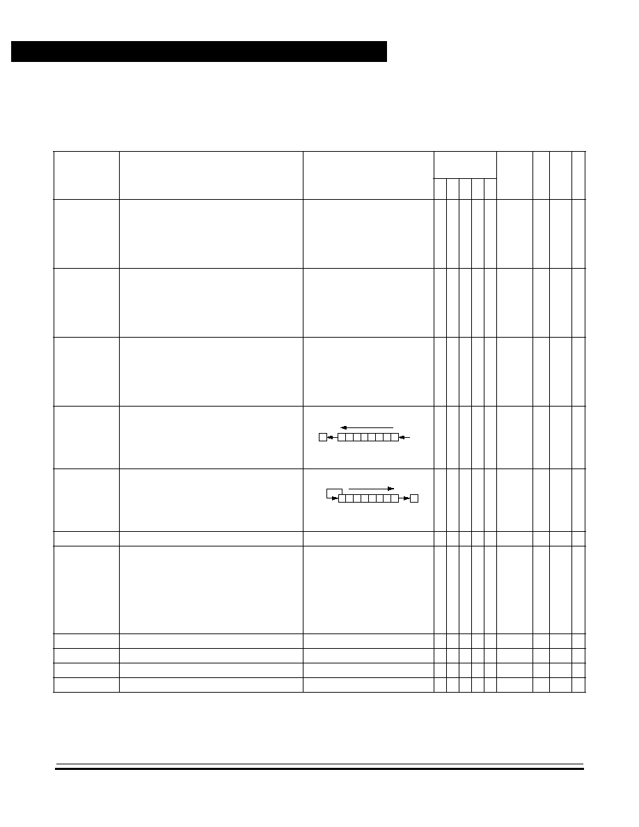
Technical Data
MC68HC705KJ1 -- Rev. 2.0
56
Central Processor Unit (CPU)
MOTOROLA
Central Processor Unit (CPU)
4.7.3 Instruction Set Summary
Table 4-6. Instruction Set Summary (Sheet 1 of 6)
Source
Form
Operation
Description
Effect on
CCR
Address
Mode
Opcode
Operand
Cycles
H I N Z C
ADC #opr
ADC opr
ADC opr
ADC opr,X
ADC opr,X
ADC ,X
Add with Carry
A
(A) + (M) + (C)
--
IMM
DIR
EXT
IX2
IX1
IX
A9
B9
C9
D9
E9
F9
ii
dd
hh ll
ee ff
ff
2
3
4
5
4
3
ADD #opr
ADD opr
ADD opr
ADD opr,X
ADD opr,X
ADD ,X
Add without Carry
A
(A) + (M)
--
IMM
DIR
EXT
IX2
IX1
IX
AB
BB
CB
DB
EB
FB
ii
dd
hh ll
ee ff
ff
2
3
4
5
4
3
AND #opr
AND opr
AND opr
AND opr,X
AND opr,X
AND ,X
Logical AND
A
(A)
(M)
-- --
--
IMM
DIR
EXT
IX2
IX1
IX
A4
B4
C4
D4
E4
F4
ii
dd
hh ll
ee ff
ff
2
3
4
5
4
3
ASL opr
ASLA
ASLX
ASL opr,X
ASL ,X
Arithmetic Shift Left (Same as LSL)
-- --
DIR
INH
INH
IX1
IX
38
48
58
68
78
dd
ff
5
3
3
6
5
ASR opr
ASRA
ASRX
ASR opr,X
ASR ,X
Arithmetic Shift Right
-- --
DIR
INH
INH
IX1
IX
37
47
57
67
77
dd
ff
5
3
3
6
5
BCC rel
Branch if Carry Bit Clear
PC
(PC) + 2 + rel ? C = 0
-- -- -- -- --
REL
24
rr
3
BCLR n opr
Clear Bit n
Mn
0
-- -- -- -- --
DIR (b0)
DIR (b1)
DIR (b2)
DIR (b3)
DIR (b4)
DIR (b5)
DIR (b6)
DIR (b7)
11
13
15
17
19
1B
1D
1F
dd
dd
dd
dd
dd
dd
dd
dd
5
5
5
5
5
5
5
5
BCS rel
Branch if Carry Bit Set (Same as BLO)
PC
(PC) + 2 + rel ? C = 1
-- -- -- -- --
REL
25
rr
3
BEQ rel
Branch if Equal
PC
(PC) + 2 + rel ? Z = 1
-- -- -- -- --
REL
27
rr
3
BHCC rel
Branch if Half-Carry Bit Clear
PC
(PC) + 2 + rel ? H = 0
-- -- -- -- --
REL
28
rr
3
BHCS rel
Branch if Half-Carry Bit Set
PC
(PC) + 2 + rel ? H = 1
-- -- -- -- --
REL
29
rr
3
C
b0
b7
0
b0
b7
C
Central Processor Unit (CPU)
Instruction Set
MC68HC705KJ1 -- Rev. 2.0
Technical Data
MOTOROLA
Central Processor Unit (CPU)
57
BHI rel
Branch if Higher
PC
(PC) + 2 + rel ? C
Z = 0
-- -- -- -- --
REL
22
rr
3
BHS rel
Branch if Higher or Same
PC
(PC) + 2 + rel ? C = 0
-- -- -- -- --
REL
24
rr
3
BIH rel
Branch if IRQ Pin High
PC
(PC) + 2 + rel ? IRQ = 1
-- -- -- -- --
REL
2F
rr
3
BIL rel
Branch if IRQ Pin Low
PC
(PC) + 2 + rel ? IRQ = 0
-- -- -- -- --
REL
2E
rr
3
BIT #opr
BIT opr
BIT opr
BIT opr,X
BIT opr,X
BIT ,X
Bit Test Accumulator with Memory Byte
(A)
(M)
-- --
--
IMM
DIR
EXT
IX2
IX1
IX
A5
B5
C5
D5
E5
F5
ii
dd
hh ll
ee ff
ff
2
3
4
5
4
3
BLO rel
Branch if Lower (Same as BCS)
PC
(PC) + 2 + rel ? C = 1
-- -- -- -- --
REL
25
rr
3
BLS rel
Branch if Lower or Same
PC
(PC) + 2 + rel ? C
Z = 1
-- -- -- -- --
REL
23
rr
3
BMC rel
Branch if Interrupt Mask Clear
PC
(PC) + 2 + rel ? I = 0
-- -- -- -- --
REL
2C
rr
3
BMI rel
Branch if Minus
PC
(PC) + 2 + rel ? N = 1
-- -- -- -- --
REL
2B
rr
3
BMS rel
Branch if Interrupt Mask Set
PC
(PC) + 2 + rel ? I = 1
-- -- -- -- --
REL
2D
rr
3
BNE rel
Branch if Not Equal
PC
(PC) + 2 + rel ? Z = 0
-- -- -- -- --
REL
26
rr
3
BPL rel
Branch if Plus
PC
(PC) + 2 + rel ? N = 0
-- -- -- -- --
REL
2A
rr
3
BRA rel
Branch Always
PC
(PC) + 2 + rel ? 1 = 1
-- -- -- -- --
REL
20
rr
3
BRCLR n opr rel Branch if Bit n Clear
PC
(PC) + 2 + rel ? Mn = 0
-- -- -- --
DIR (b0)
DIR (b1)
DIR (b2)
DIR (b3)
DIR (b4)
DIR (b5)
DIR (b6)
DIR (b7)
01
03
05
07
09
0B
0D
0F
dd rr
dd rr
dd rr
dd rr
dd rr
dd rr
dd rr
dd rr
5
5
5
5
5
5
5
5
BRN rel
Branch Never
PC
(PC) + 2 + rel ? 1 = 0
-- -- -- -- --
REL
21
rr
3
BRSET n opr rel Branch if Bit n Set
PC
(PC) + 2 + rel ? Mn = 1
-- -- -- --
DIR (b0)
DIR (b1)
DIR (b2)
DIR (b3)
DIR (b4)
DIR (b5)
DIR (b6)
DIR (b7)
00
02
04
06
08
0A
0C
0E
dd rr
dd rr
dd rr
dd rr
dd rr
dd rr
dd rr
dd rr
5
5
5
5
5
5
5
5
BSET n opr
Set Bit n
Mn
1
-- -- -- -- --
DIR (b0)
DIR (b1)
DIR (b2)
DIR (b3)
DIR (b4)
DIR (b5)
DIR (b6)
DIR (b7)
10
12
14
16
18
1A
1C
1E
dd
dd
dd
dd
dd
dd
dd
dd
5
5
5
5
5
5
5
5
Table 4-6. Instruction Set Summary (Sheet 2 of 6)
Source
Form
Operation
Description
Effect on
CCR
Address
Mode
Opcode
Operand
Cycles
H I N Z C
Technical Data
MC68HC705KJ1 -- Rev. 2.0
58
Central Processor Unit (CPU)
MOTOROLA
Central Processor Unit (CPU)
BSR rel
Branch to Subroutine
PC
(PC) + 2; push (PCL)
SP
(SP) ≠ 1; push (PCH)
SP
(SP) ≠ 1
PC
(PC) + rel
-- -- -- -- --
REL
AD
rr
6
CLC
Clear Carry Bit
C
0
-- -- -- -- 0
INH
98
2
CLI
Clear Interrupt Mask
I
0
-- 0 -- -- --
INH
9A
2
CLR opr
CLRA
CLRX
CLR opr,X
CLR ,X
Clear Byte
M
$00
A
$00
X
$00
M
$00
M
$00
-- -- 0
1 --
DIR
INH
INH
IX1
IX
3F
4F
5F
6F
7F
dd
ff
5
3
3
6
5
CMP #opr
CMP opr
CMP opr
CMP opr,X
CMP opr,X
CMP ,X
Compare Accumulator with Memory Byte
(A) ≠ (M)
-- --
IMM
DIR
EXT
IX2
IX1
IX
A1
B1
C1
D1
E1
F1
ii
dd
hh ll
ee ff
ff
2
3
4
5
4
3
COM opr
COMA
COMX
COM opr,X
COM ,X
Complement Byte (One's Complement)
M
(
M
) = $FF ≠ (M)
A
(
A
) = $FF ≠ (A)
X
(
X
) = $FF ≠ (X)
M
(
M
) = $FF ≠ (M)
M
(
M
) = $FF ≠ (M)
-- --
1
DIR
INH
INH
IX1
IX
33
43
53
63
73
dd
ff
5
3
3
6
5
CPX #opr
CPX opr
CPX opr
CPX opr,X
CPX opr,X
CPX ,X
Compare Index Register with Memory Byte
(X) ≠ (M)
-- --
IMM
DIR
EXT
IX2
IX1
IX
A3
B3
C3
D3
E3
F3
ii
dd
hh ll
ee ff
ff
2
3
4
5
4
3
DEC opr
DECA
DECX
DEC opr,X
DEC ,X
Decrement Byte
M
(M) ≠ 1
A
(A) ≠ 1
X
(X) ≠ 1
M
(M) ≠ 1
M
(M) ≠ 1
-- --
--
DIR
INH
INH
IX1
IX
3A
4A
5A
6A
7A
dd
ff
5
3
3
6
5
EOR #opr
EOR opr
EOR opr
EOR opr,X
EOR opr,X
EOR ,X
EXCLUSIVE OR Accumulator with Memory Byte
A
(A)
(M)
-- --
--
IMM
DIR
EXT
IX2
IX1
IX
A8
B8
C8
D8
E8
F8
ii
dd
hh ll
ee ff
ff
2
3
4
5
4
3
INC opr
INCA
INCX
INC opr,X
INC ,X
Increment Byte
M
(M) + 1
A
(A) + 1
X
(X) + 1
M
(M) + 1
M
(M) + 1
-- --
--
DIR
INH
INH
IX1
IX
3C
4C
5C
6C
7C
dd
ff
5
3
3
6
5
Table 4-6. Instruction Set Summary (Sheet 3 of 6)
Source
Form
Operation
Description
Effect on
CCR
Address
Mode
Opcode
Operand
Cycles
H I N Z C
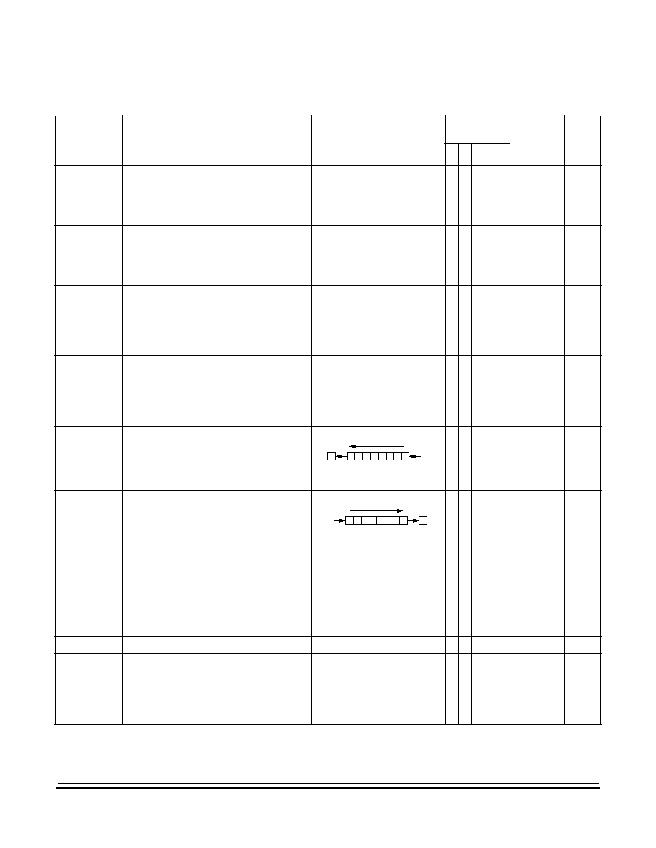
Central Processor Unit (CPU)
Instruction Set
MC68HC705KJ1 -- Rev. 2.0
Technical Data
MOTOROLA
Central Processor Unit (CPU)
59
JMP opr
JMP opr
JMP opr,X
JMP opr,X
JMP ,X
Unconditional Jump
PC
Jump Address
-- -- -- -- --
DIR
EXT
IX2
IX1
IX
BC
CC
DC
EC
FC
dd
hh ll
ee ff
ff
2
3
4
3
2
JSR opr
JSR opr
JSR opr,X
JSR opr,X
JSR ,X
Jump to Subroutine
PC
(PC) + n (n = 1, 2, or 3)
Push (PCL); SP
(SP) ≠ 1
Push (PCH); SP
(SP) ≠ 1
PC
Effective Address
-- -- -- -- --
DIR
EXT
IX2
IX1
IX
BD
CD
DD
ED
FD
dd
hh ll
ee ff
ff
5
6
7
6
5
LDA #opr
LDA opr
LDA opr
LDA opr,X
LDA opr,X
LDA ,X
Load Accumulator with Memory Byte
A
(M)
-- --
--
IMM
DIR
EXT
IX2
IX1
IX
A6
B6
C6
D6
E6
F6
ii
dd
hh ll
ee ff
ff
2
3
4
5
4
3
LDX #opr
LDX opr
LDX opr
LDX opr,X
LDX opr,X
LDX ,X
Load Index Register with Memory Byte
X
(M)
-- --
--
IMM
DIR
EXT
IX2
IX1
IX
AE
BE
CE
DE
EE
FE
ii
dd
hh ll
ee ff
ff
2
3
4
5
4
3
LSL opr
LSLA
LSLX
LSL opr,X
LSL ,X
Logical Shift Left (Same as ASL)
-- --
DIR
INH
INH
IX1
IX
38
48
58
68
78
dd
ff
5
3
3
6
5
LSR opr
LSRA
LSRX
LSR opr,X
LSR ,X
Logical Shift Right
-- -- 0
DIR
INH
INH
IX1
IX
34
44
54
64
74
dd
ff
5
3
3
6
5
MUL
Unsigned Multiply
X : A
(X)
◊
(A)
0 -- -- -- 0
INH
42
11
NEG opr
NEGA
NEGX
NEG opr,X
NEG ,X
Negate Byte (Two's Complement)
M
≠(M) = $00 ≠ (M)
A
≠(A) = $00 ≠ (A)
X
≠(X) = $00 ≠ (X)
M
≠(M) = $00 ≠ (M)
M
≠(M) = $00 ≠ (M)
-- --
DIR
INH
INH
IX1
IX
30
40
50
60
70
dd
ff
5
3
3
6
5
NOP
No Operation
-- -- -- -- --
INH
9D
2
ORA #opr
ORA opr
ORA opr
ORA opr,X
ORA opr,X
ORA ,X
Logical OR Accumulator with Memory
A
(A)
(M)
-- --
--
IMM
DIR
EXT
IX2
IX1
IX
AA
BA
CA
DA
EA
FA
ii
dd
hh ll
ee ff
ff
2
3
4
5
4
3
Table 4-6. Instruction Set Summary (Sheet 4 of 6)
Source
Form
Operation
Description
Effect on
CCR
Address
Mode
Opcode
Operand
Cycles
H I N Z C
C
b0
b7
0
b0
b7
C
0
Technical Data
MC68HC705KJ1 -- Rev. 2.0
60
Central Processor Unit (CPU)
MOTOROLA
Central Processor Unit (CPU)
ROL opr
ROLA
ROLX
ROL opr,X
ROL ,X
Rotate Byte Left through Carry Bit
-- --
DIR
INH
INH
IX1
IX
39
49
59
69
79
dd
ff
5
3
3
6
5
ROR opr
RORA
RORX
ROR opr,X
ROR ,X
Rotate Byte Right through Carry Bit
-- --
DIR
INH
INH
IX1
IX
36
46
56
66
76
dd
ff
5
3
3
6
5
RSP
Reset Stack Pointer
SP
$00FF
-- -- -- -- --
INH
9C
2
RTI
Return from Interrupt
SP
(SP) + 1; Pull (CCR)
SP
(SP) + 1; Pull (A)
SP
(SP) + 1; Pull (X)
SP
(SP) + 1; Pull (PCH)
SP
(SP) + 1; Pull (PCL)
INH
80
9
RTS
Return from Subroutine
SP
(SP) + 1; Pull (PCH)
SP
(SP) + 1; Pull (PCL)
-- -- -- -- --
INH
81
6
SBC #opr
SBC opr
SBC opr
SBC opr,X
SBC opr,X
SBC ,X
Subtract Memory Byte and Carry Bit from
Accumulator
A
(A) ≠ (M) ≠ (C)
-- --
IMM
DIR
EXT
IX2
IX1
IX
A2
B2
C2
D2
E2
F2
ii
dd
hh ll
ee ff
ff
2
3
4
5
4
3
SEC
Set Carry Bit
C
1
-- -- -- -- 1
INH
99
2
SEI
Set Interrupt Mask
I
1
-- 1 -- -- --
INH
9B
2
STA opr
STA opr
STA opr,X
STA opr,X
STA ,X
Store Accumulator in Memory
M
(A)
-- --
--
DIR
EXT
IX2
IX1
IX
B7
C7
D7
E7
F7
dd
hh ll
ee ff
ff
4
5
6
5
4
STOP
Stop Oscillator and Enable IRQ Pin
-- 0 -- -- --
INH
8E
2
STX opr
STX opr
STX opr,X
STX opr,X
STX ,X
Store Index Register In Memory
M
(X)
-- --
--
DIR
EXT
IX2
IX1
IX
BF
CF
DF
EF
FF
dd
hh ll
ee ff
ff
4
5
6
5
4
SUB #opr
SUB opr
SUB opr
SUB opr,X
SUB opr,X
SUB ,X
Subtract Memory Byte from Accumulator
A
(A) ≠ (M)
-- --
IMM
DIR
EXT
IX2
IX1
IX
A0
B0
C0
D0
E0
F0
ii
dd
hh ll
ee ff
ff
2
3
4
5
4
3
Table 4-6. Instruction Set Summary (Sheet 5 of 6)
Source
Form
Operation
Description
Effect on
CCR
Address
Mode
Opcode
Operand
Cycles
H I N Z C
C
b0
b7
b0
b7
C
Central Processor Unit (CPU)
Instruction Set
MC68HC705KJ1 -- Rev. 2.0
Technical Data
MOTOROLA
Central Processor Unit (CPU)
61
SWI
Software Interrupt
PC
(PC) + 1; Push (PCL)
SP
(SP) ≠ 1; Push (PCH)
SP
(SP) ≠ 1; Push (X)
SP
(SP) ≠ 1; Push (A)
SP
(SP) ≠ 1; Push (CCR)
SP
(SP) ≠ 1; I
1
PCH
Interrupt Vector High Byte
PCL
Interrupt Vector Low Byte
-- 1 -- -- --
INH
83
10
TAX
Transfer Accumulator to Index Register
X
(A)
-- -- -- -- --
INH
97
2
TST opr
TSTA
TSTX
TST opr,X
TST ,X
Test Memory Byte for Negative or Zero
(M) ≠ $00
-- --
--
DIR
INH
INH
IX1
IX
3D
4D
5D
6D
7D
dd
ff
4
3
3
5
4
TXA
Transfer Index Register to Accumulator
A
(X)
-- -- -- -- --
INH
9F
2
WAIT
Stop CPU Clock and Enable Interrupts
-- 0 -- -- --
INH
8F
2
A
Accumulator
opr
Operand (one or two bytes)
C
Carry/borrow flag
PC
Program counter
CCR
Condition code register
PCH
Program counter high byte
dd
Direct address of operand
PCL
Program counter low byte
dd rr
Direct address of operand and relative offset of branch instruction
REL
Relative addressing mode
DIR
Direct addressing mode
rel
Relative program counter offset byte
ee ff
High and low bytes of offset in indexed, 16-bit offset addressing
rr
Relative program counter offset byte
EXT
Extended addressing mode
SP
Stack pointer
ff
Offset byte in indexed, 8-bit offset addressing
X
Index register
H
Half-carry flag
Z
Zero flag
hh ll
High and low bytes of operand address in extended addressing
#
Immediate value
I
Interrupt mask
Logical AND
ii
Immediate operand byte
Logical OR
IMM
Immediate addressing mode
Logical EXCLUSIVE OR
INH
Inherent addressing mode
( )
Contents of
IX
Indexed, no offset addressing mode
≠( )
Negation (two's complement)
IX1
Indexed, 8-bit offset addressing mode
Loaded with
IX2
Indexed, 16-bit offset addressing mode
?
If
M
Memory location
:
Concatenated with
N
Negative flag
Set or cleared
n
Any bit
--
Not affected
Table 4-6. Instruction Set Summary (Sheet 6 of 6)
Source
Form
Operation
Description
Effect on
CCR
Address
Mode
Opcode
Operand
Cycles
H I N Z C
T
echnical Data
MC68HC705KJ1 --
R
e
v
. 2.0
62
Central Processor Unit (CPU)
MOTOROLA
Central Pr
ocessor Unit (CPU)
Table 4-7. Opcode Map
Bit Manipulation
Branch
Read-Modify-Write
Control
Register/Memory
DIR
DIR
REL
DIR
INH
INH
IX1
IX
INH
INH
IMM
DIR
EXT
IX2
IX1
IX
0
1
2
3
4
5
6
7
8
9
A
B
C
D
E
F
0
5
BRSET0
3
DIR
5
BSET0
2
DIR
3
BRA
2
REL
5
NEG
2
DIR
3
NEGA
1
INH
3
NEGX
1
INH
6
NEG
2
IX1
5
NEG
1
IX
9
RTI
1
INH
2
SUB
2
IMM
3
SUB
2
DIR
4
SUB
3
EXT
5
SUB
3
IX2
4
SUB
2
IX1
3
SUB
1
IX
0
1
5
BRCLR0
3
DIR
5
BCLR0
2
DIR
3
BRN
2
REL
6
RTS
1
INH
2
CMP
2
IMM
3
CMP
2
DIR
4
CMP
3
EXT
5
CMP
3
IX2
4
CMP
2
IX1
3
CMP
1
IX
1
2
5
BRSET1
3
DIR
5
BSET1
2
DIR
3
BHI
2
REL
11
MUL
1
INH
2
SBC
2
IMM
3
SBC
2
DIR
4
SBC
3
EXT
5
SBC
3
IX2
4
SBC
2
IX1
3
SBC
1
IX
2
3
5
BRCLR1
3
DIR
5
BCLR1
2
DIR
3
BLS
2
REL
5
COM
2
DIR
3
COMA
1
INH
3
COMX
1
INH
6
COM
2
IX1
5
COM
1
IX
10
SWI
1
INH
2
CPX
2
IMM
3
CPX
2
DIR
4
CPX
3
EXT
5
CPX
3
IX2
4
CPX
2
IX1
3
CPX
1
IX
3
4
5
BRSET2
3
DIR
5
BSET2
2
DIR
3
BCC
2
REL
5
LSR
2
DIR
3
LSRA
1
INH
3
LSRX
1
INH
6
LSR
2
IX1
5
LSR
1
IX
2
AND
2
IMM
3
AND
2
DIR
4
AND
3
EXT
5
AND
3
IX2
4
AND
2
IX1
3
AND
1
IX
4
5
5
BRCLR2
3
DIR
5
BCLR2
2
DIR
3
BCS/BLO
2
REL
2
BIT
2
IMM
3
BIT
2
DIR
4
BIT
3
EXT
5
BIT
3
IX2
4
BIT
2
IX1
3
BIT
1
IX
5
6
5
BRSET3
3
DIR
5
BSET3
2
DIR
3
BNE
2
REL
5
ROR
2
DIR
3
RORA
1
INH
3
RORX
1
INH
6
ROR
2
IX1
5
ROR
1
IX
2
LDA
2
IMM
3
LDA
2
DIR
4
LDA
3
EXT
5
LDA
3
IX2
4
LDA
2
IX1
3
LDA
1
IX
6
7
5
BRCLR3
3
DIR
5
BCLR3
2
DIR
3
BEQ
2
REL
5
ASR
2
DIR
3
ASRA
1
INH
3
ASRX
1
INH
6
ASR
2
IX1
5
ASR
1
IX
2
TAX
1
INH
4
STA
2
DIR
5
STA
3
EXT
6
STA
3
IX2
5
STA
2
IX1
4
STA
1
IX
7
8
5
BRSET4
3
DIR
5
BSET4
2
DIR
3
BHCC
2
REL
5
ASL/LSL
2
DIR
3
ASLA/LSLA
1
INH
3
ASLX/LSLX
1
INH
6
ASL/LSL
2
IX1
5
ASL/LSL
1
IX
2
CLC
1
INH
2
EOR
2
IMM
3
EOR
2
DIR
4
EOR
3
EXT
5
EOR
3
IX2
4
EOR
2
IX1
3
EOR
1
IX
8
9
5
BRCLR4
3
DIR
5
BCLR4
2
DIR
3
BHCS
2
REL
5
ROL
2
DIR
3
ROLA
1
INH
3
ROLX
1
INH
6
ROL
2
IX1
5
ROL
1
IX
2
SEC
1
INH
2
ADC
2
IMM
3
ADC
2
DIR
4
ADC
3
EXT
5
ADC
3
IX2
4
ADC
2
IX1
3
ADC
1
IX
9
A
5
BRSET5
3
DIR
5
BSET5
2
DIR
3
BPL
2
REL
5
DEC
2
DIR
3
DECA
1
INH
3
DECX
1
INH
6
DEC
2
IX1
5
DEC
1
IX
2
CLI
1
INH
2
ORA
2
IMM
3
ORA
2
DIR
4
ORA
3
EXT
5
ORA
3
IX2
4
ORA
2
IX1
3
ORA
1
IX
A
B
5
BRCLR5
3
DIR
5
BCLR5
2
DIR
3
BMI
2
REL
2
SEI
1
INH
2
ADD
2
IMM
3
ADD
2
DIR
4
ADD
3
EXT
5
ADD
3
IX2
4
ADD
2
IX1
3
ADD
1
IX
B
C
5
BRSET6
3
DIR
5
BSET6
2
DIR
3
BMC
2
REL
5
INC
2
DIR
3
INCA
1
INH
3
INCX
1
INH
6
INC
2
IX1
5
INC
1
IX
2
RSP
1
INH
2
JMP
2
DIR
3
JMP
3
EXT
4
JMP
3
IX2
3
JMP
2
IX1
2
JMP
1
IX
C
D
5
BRCLR6
3
DIR
5
BCLR6
2
DIR
3
BMS
2
REL
4
TST
2
DIR
3
TSTA
1
INH
3
TSTX
1
INH
5
TST
2
IX1
4
TST
1
IX
2
NOP
1
INH
6
BSR
2
REL
5
JSR
2
DIR
6
JSR
3
EXT
7
JSR
3
IX2
6
JSR
2
IX1
5
JSR
1
IX
D
E
5
BRSET7
3
DIR
5
BSET7
2
DIR
3
BIL
2
REL
2
STOP
1
INH
2
LDX
2
IMM
3
LDX
2
DIR
4
LDX
3
EXT
5
LDX
3
IX2
4
LDX
2
IX1
3
LDX
1
IX
E
F
5
BRCLR7
3
DIR
5
BCLR7
2
DIR
3
BIH
2
REL
5
CLR
2
DIR
3
CLRA
1
INH
3
CLRX
1
INH
6
CLR
2
IX1
5
CLR
1
IX
2
WAIT
1
INH
2
TXA
1
INH
4
STX
2
DIR
5
STX
3
EXT
6
STX
3
IX2
5
STX
2
IX1
4
STX
1
IX
F
INH = Inherent
REL = Relative
IMM = Immediate IX = Indexed, No Offset
DIR = Direct
IX1 = Indexed, 8-Bit Offset
EXT = Extended IX2 = Indexed, 16-Bit Offset
0
MSB of Opcode in
Hexadecimal
LSB of Opcode in Hexadecimal
0
5
BRSET0
3
DIR
Number of Cycles
Opcode Mnemonic
Number of Bytes/Addressing Mode
LSB
MSB
LSB
MSB
LSB
MSB

MC68HC705KJ1 -- Rev. 2.0
Technical Data
MOTOROLA
Resets and Interrupts
63
Technical Data -- MC68HC705KJ1
Section 5. Resets and Interrupts
5.1 Contents
5.2
Introduction . . . . . . . . . . . . . . . . . . . . . . . . . . . . . . . . . . . . . . . .63
5.3
Resets. . . . . . . . . . . . . . . . . . . . . . . . . . . . . . . . . . . . . . . . . . . .64
5.3.1
Power-On Reset . . . . . . . . . . . . . . . . . . . . . . . . . . . . . . . . . .64
5.3.2
External Reset . . . . . . . . . . . . . . . . . . . . . . . . . . . . . . . . . . .65
5.3.3
COP Watchdog Reset . . . . . . . . . . . . . . . . . . . . . . . . . . . . .66
5.3.4
Illegal Address Reset . . . . . . . . . . . . . . . . . . . . . . . . . . . . . .66
5.4
Interrupts. . . . . . . . . . . . . . . . . . . . . . . . . . . . . . . . . . . . . . . . . .66
5.4.1
Software Interrupt . . . . . . . . . . . . . . . . . . . . . . . . . . . . . . . . .66
5.4.2
External Interrupt . . . . . . . . . . . . . . . . . . . . . . . . . . . . . . . . .67
5.4.3
Timer Interrupts . . . . . . . . . . . . . . . . . . . . . . . . . . . . . . . . . .69
5.4.3.1
Real-Time Interrupt . . . . . . . . . . . . . . . . . . . . . . . . . . . . .69
5.4.3.2
Timer Overflow Interrupt . . . . . . . . . . . . . . . . . . . . . . . . .69
5.4.4
Interrupt Processing . . . . . . . . . . . . . . . . . . . . . . . . . . . . . . .69
5.2 Introduction
Reset initializes the MCU by returning the program counter to a known
address and by forcing control and status bits to known states.
Interrupts temporarily change the sequence of program execution to
respond to events that occur during processing.
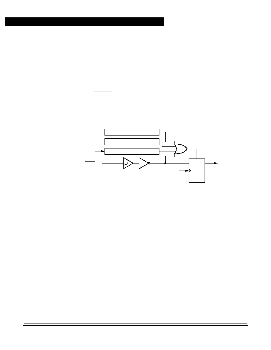
Technical Data
MC68HC705KJ1 -- Rev. 2.0
64
Resets and Interrupts
MOTOROLA
Resets and Interrupts
5.3 Resets
A reset immediately stops the operation of the instruction being
executed, initializes certain control and status bits, and loads the
program counter with a user-defined reset vector address. The following
sources can generate a reset:
∑
Power-on reset (POR) circuit
∑
RESET pin
∑
Computer operating properly (COP) watchdog
∑
Illegal address
Figure 5-1. Reset Sources
5.3.1 Power-On Reset
A positive transition on the V
DD
pin generates a power-on reset.
NOTE:
The power-on reset is strictly for power-up conditions and cannot be
used to detect drops in power supply voltage.
A 4064-t
cyc
(internal clock cycle) delay after the oscillator becomes
active allows the clock generator to stabilize. If any reset source is active
at the end of this delay, the MCU remains in the reset condition until all
reset sources are inactive.
D
Q
CK
S
RESET
LATCH
INTERNAL CLOCK
RST
TO CPU AND
RESET PIN
V
DD
PERIPHERAL
MODULES
ILLEGAL ADDRESS
COP WATCHDOG
POWER-ON RESET
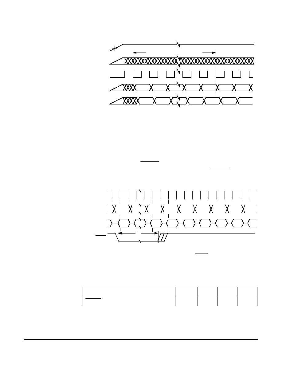
Resets and Interrupts
Resets
MC68HC705KJ1 -- Rev. 2.0
Technical Data
MOTOROLA
Resets and Interrupts
65
Figure 5-2. Power-On Reset Timing
5.3.2 External Reset
A logic 0 applied to the RESET pin for 1 1/2 t
cyc
generates an external
reset. A Schmitt trigger senses the logic level at the RESET pin.
Figure 5-3. External Reset Timing
OSCILLATOR STABILIZATION DELAY
(2)
V
DD
OSC1 PIN
INTERNAL
CLOCK
INTERNAL
ADDRESS BUS
Notes:
INTERNAL
DATA BUS
1. Power-on reset threshold is typically between 1 V and 2 V.
2. 4064 cycles or 128 cycles, depending on state of SOSCD bit in MOR
$07FE
$07FE
$07FE
$07FE
$07FE
$07FE
$07FF
NEW PCH
NEW PCL
(NOTE 1)
3. Internal clock, internal address bus, and internal data bus are not available externally.
Table 5-1. External Reset Timing
Characteristic
Symbol
Min
Max
Unit
RESET Pulse Width
t
RL
1.5
--
t
cyc
INTERNAL
CLOCK
INTERNAL
ADDRESS BUS
Notes:
INTERNAL
DATA BUS
$07FE
$07FE
$07FE
$07FE
$07FF
NEW PC
1. Internal clock, internal address bus, and internal data bus are not available externally.
2. The next rising edge of the internal clock after the rising edge of RESET initiates the reset sequence.
NEW
PCH
t
RL
NEW PC
NEW
PCL
DUMMY
OP
CODE
RESET

Technical Data
MC68HC705KJ1 -- Rev. 2.0
66
Resets and Interrupts
MOTOROLA
Resets and Interrupts
5.3.3 COP Watchdog Reset
A timeout of the COP watchdog generates a COP reset. The COP
watchdog is part of a software error detection system and must be
cleared periodically to start a new timeout period. To clear the COP
watchdog and prevent a COP reset, write a logic 0 to bit 0 (COPC) of the
COP register at location $07F0.
5.3.4 Illegal Address Reset
An opcode fetch from an address not in RAM or EPROM generates a
reset.
5.4 Interrupts
The following sources can generate interrupts:
∑
SWI instruction
∑
External interrupt pins
≠
IRQ/V
PP
pin
≠
PA0≠PA3 pins
∑
Timer
≠
Real-time interrupt flag (RTIF)
≠
Timer overflow flag (TOF)
An interrupt temporarily stops the program sequence to process a
particular event. An interrupt does not stop the operation of the
instruction being executed, but takes effect when the current instruction
completes its execution. Interrupt processing automatically saves the
CPU registers on the stack and loads the program counter with a
user-defined interrupt vector address.
5.4.1 Software Interrupt
The software interrupt (SWI) instruction causes a non-maskable
interrupt.
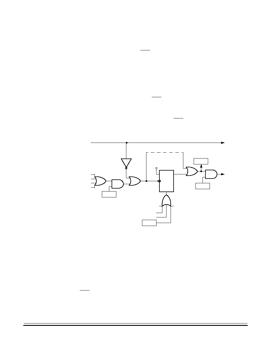
Resets and Interrupts
Interrupts
MC68HC705KJ1 -- Rev. 2.0
Technical Data
MOTOROLA
Resets and Interrupts
67
5.4.2 External Interrupt
An interrupt signal on the IRQ/V
PP
pin latches an external interrupt
request. When the CPU completes its current instruction, it tests the IRQ
latch. If the IRQ latch is set, the CPU then tests the I bit in the condition
code register. If the I bit is clear, the CPU then begins the interrupt
sequence.
The CPU clears the IRQ latch during interrupt processing, so that
another interrupt signal on the IRQ/V
PP
pin can latch another interrupt
request during the interrupt service routine. As soon as the I bit is
cleared during the return from interrupt, the CPU can recognize the new
interrupt request.
Figure 5-4
shows the IRQ/V
PP
pin interrupt logic.
Figure 5-4. External Interrupt Logic
Setting the I bit in the condition code register disables external interrupts.
The port A external interrupt bit (PIRQ) in the mask option register
enables pins PA0≠PA3 to function as external interrupt pins.
The external interrupt sensitivity bit (LEVEL) in the mask option register
controls interrupt triggering sensitivity of external interrupt pins. The
IRQ/V
PP
pin can be negative-edge triggered only or negative-edge and
low-level triggered. Port A external interrupt pins can be positive-edge
PIRQ
LEVEL-SENSITIVE TRIGGER
PA3
PA2
PA1
IRQ
PA0
V
DD
(MOR LEVEL BIT)
RESET
IRQ VECTOR FETCH
EXTERNAL
INTERRUPT
REQUEST
(MOR)
TO BIH & BIL
INSTRUCTION
PROCESSING
IRQF
IRQR
IRQE
D
Q
CK
IRQ
CLR
LATCH
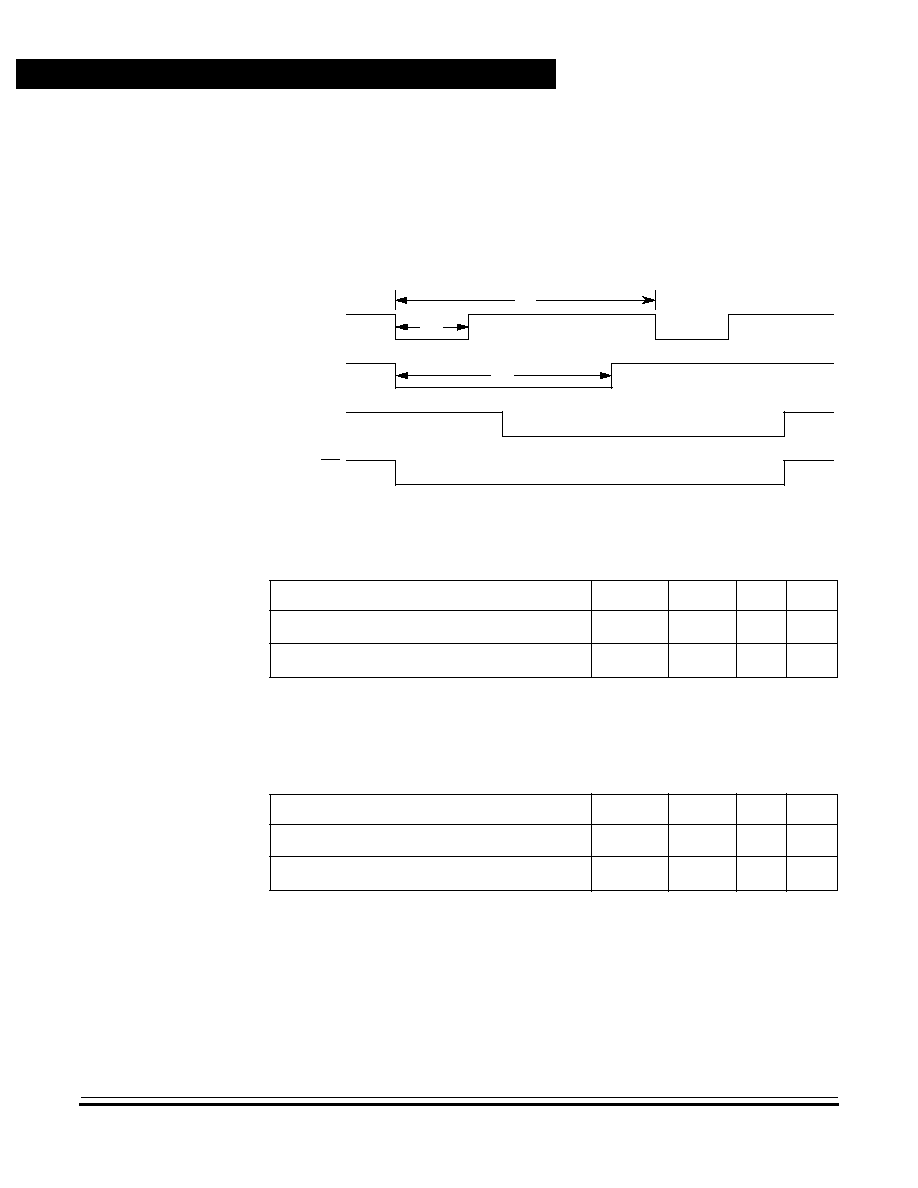
Technical Data
MC68HC705KJ1 -- Rev. 2.0
68
Resets and Interrupts
MOTOROLA
Resets and Interrupts
triggered only or both positive-edge and high-level triggered. The
level-sensitive triggering option allows multiple external interrupt
sources to be wire-ORed to an external interrupt pin. An external
interrupt request, shown in
Figure 5-5
, is latched as long as any source
is holding an external interrupt pin low.
Figure 5-5. External Interrupt Timing
Table 5-2. External Interrupt Timing (V
DD
= 5.0 Vdc)
(1)
1. V
DD
= 5.0 Vdc
±
10%, V
SS
= 0 Vdc, T
A
= ≠40
∞
C to +85
∞
C, unless otherwise noted.
Characteristic
Symbol
Min
Max
Unit
Interrupt Pulse Width Low (Edge-Triggered)
t
ILIH
125
--
ns
Interrupt Pulse Period
t
ILIL
Note
(2)
2. The minimum t
ILIL
should not be less than the number of interrupt service routine cycles
plus 19
t
cyc
.
--
t
cyc
Table 5-3. External Interrupt Timing (V
DD
= 3.3 Vdc)
(1)
1. V
DD
= 3.3 Vdc
±
10%, V
SS
= 0 Vdc, T
A
= ≠40
∞
C to +85
∞
C unless otherwise noted.
Characteristic
Symbol
Min
Max
Unit
Interrupt Pulse Width Low (Edge-Triggered)
t
ILIH
250
--
ns
Interrupt Pulse Period
t
ILIL
Note
(2)
2. The minimum t
ILIL
should not be less than the number of interrupt service routine cycles
plus 19
t
cyc
.
--
t
cyc
IRQ
t
ILIH
t
ILIL
t
ILIH
EXT. INT. PIN
EXT. INT. PIN
1
EXT. INT. PIN
n
.
.
.
(INTERNAL)

Resets and Interrupts
Interrupts
MC68HC705KJ1 -- Rev. 2.0
Technical Data
MOTOROLA
Resets and Interrupts
69
5.4.3 Timer Interrupts
The timer can generate the following interrupt requests:
∑
Real time
∑
Timer overflow
Setting the I bit in the condition code register disables timer interrupts.
5.4.3.1 Real-Time Interrupt
A real-time interrupt occurs if the real-time interrupt flag, RTIF, becomes
set while the real-time interrupt enable bit, RTIE, is also set. RTIF and
RTIE are in the timer status and control register.
5.4.3.2 Timer Overflow Interrupt
A timer overflow interrupt request occurs if the timer overflow flag, TOF,
becomes set while the timer overflow interrupt enable bit, TOIE, is also
set. TOF and TOIE are in the timer status and control register.
5.4.4 Interrupt Processing
The CPU takes the following actions to begin servicing an interrupt:
∑
Stores the CPU registers on the stack in the order shown in
Figure 5-6
∑
Sets the I bit in the condition code register to prevent further
interrupts
∑
Loads the program counter with the contents of the appropriate
interrupt vector locations:
≠
$07FC and $07FD (software interrupt vector)
≠
$07FA and $07FB (external interrupt vector)
≠
$07F8 and $07F9 (timer interrupt vector)
The return-from-interrupt (RTI) instruction causes the CPU to recover
the CPU registers from the stack as shown in
Figure 5-6
.
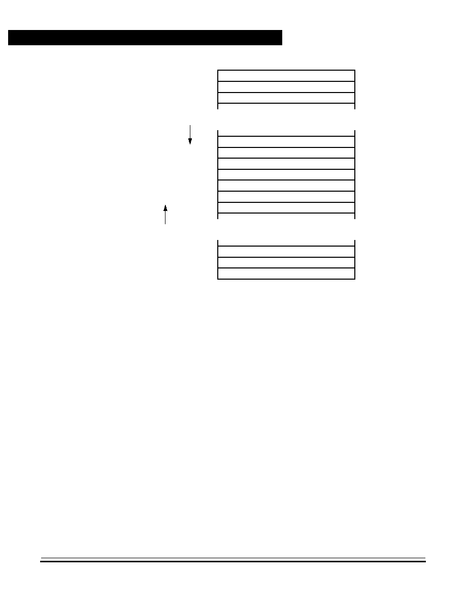
Technical Data
MC68HC705KJ1 -- Rev. 2.0
70
Resets and Interrupts
MOTOROLA
Resets and Interrupts
Figure 5-6. Interrupt Stacking Order
CONDITION CODE REGISTER
$00C0 (BOTTOM OF STACK)
$00C1
$00C2
∑
∑
∑
ACCUMULATOR
INDEX REGISTER
PROGRAM COUNTER (HIGH BYTE)
PROGRAM COUNTER (LOW BYTE)
∑
∑
∑
∑
∑
∑
∑
∑
∑
$00FD
$00FE
$00FF (TOP OF STACK)
1
2
3
4
5
5
4
3
2
1
UNSTACKING
ORDER
STACKING
ORDER
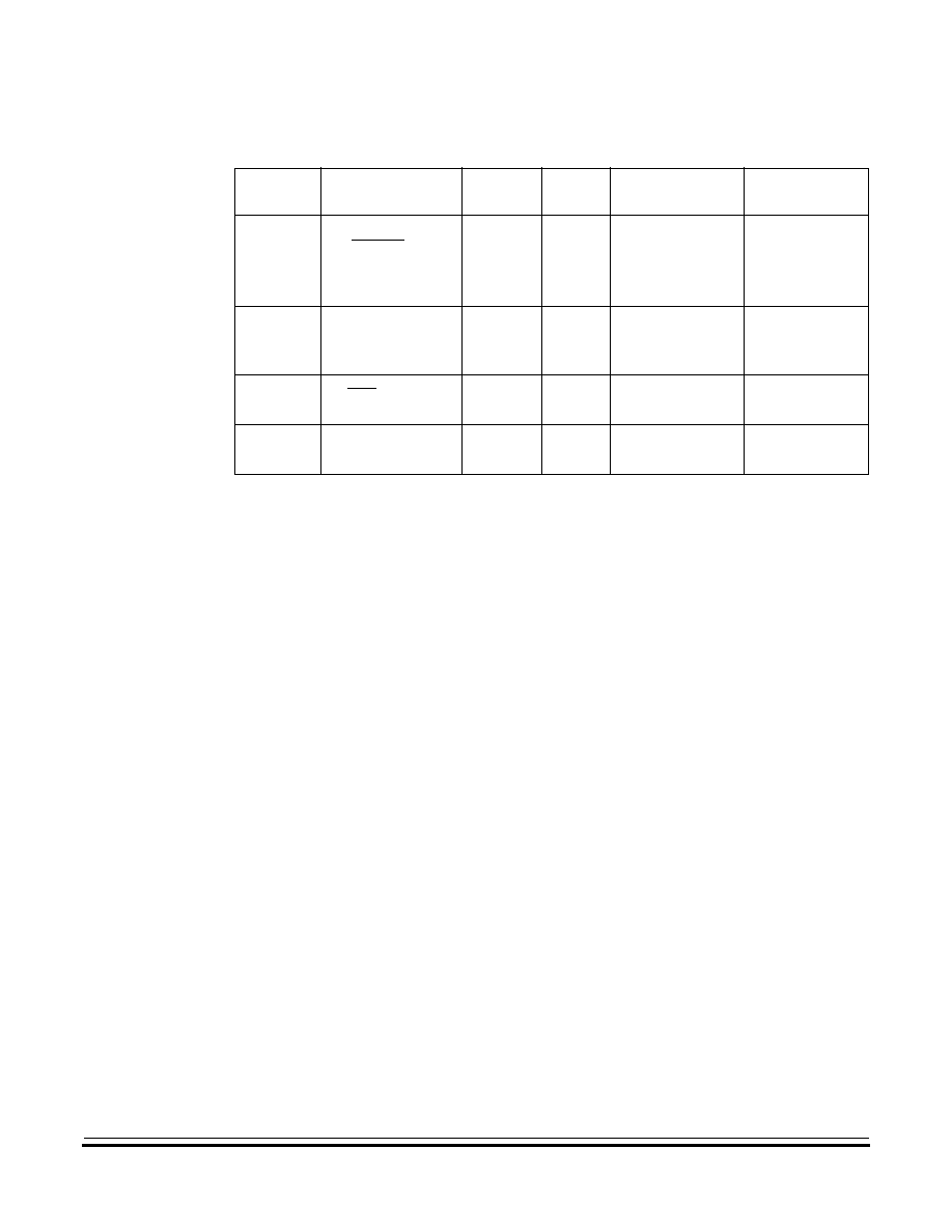
Resets and Interrupts
Interrupts
MC68HC705KJ1 -- Rev. 2.0
Technical Data
MOTOROLA
Resets and Interrupts
71
Table 5-4. Reset/Interrupt Vector Addresses
Function
Source
Local
Mask
Global
Mask
Priority
(1 = Highest)
Vector
Address
Reset
Power-On
RESET Pin
COP Watchdog
(1)
Illegal Address
None
None
1
$07FE
≠
$07FF
Software
Interrupt
(SWI)
User Code
None
None
Same Priority
as Instruction
$07FC
≠
$07FD
External
Interrupt
IRQ/V
PP
Pin
IRQE
I Bit
2
$07FA
≠
$07FB
Timer
Interrupts
RTIF Bit
TOF Bit
RTIE Bit
TOIE Bit
I Bit
3
$07F8
≠
$07F9
1. The COP watchdog is programmable in the mask option register.
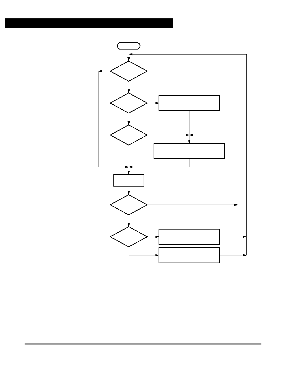
Technical Data
MC68HC705KJ1 -- Rev. 2.0
72
Resets and Interrupts
MOTOROLA
Resets and Interrupts
Figure 5-7. Interrupt Flowchart
EXTERNAL
INTERRUPT?
I BIT SET?
TIMER
INTERRUPT?
FETCH NEXT
INSTRUCTION.
SWI
INSTRUCTION?
RTI
INSTRUCTION?
STACK PC, X, A, CCR.
SET I BIT.
LOAD PC WITH INTERRUPT VECTOR.
YES
YES
YES
YES
YES
UNSTACK CCR, A, X, PC.
EXECUTE INSTRUCTION.
CLEAR IRQ LATCH.
NO
NO
NO
NO
NO
FROM RESET

MC68HC705KJ1 -- Rev. 2.0
Technical Data
MOTOROLA
Low-Power Modes
73
Technical Data -- MC68HC705KJ1
Section 6. Low-Power Modes
6.1 Contents
6.2
Introduction . . . . . . . . . . . . . . . . . . . . . . . . . . . . . . . . . . . . . . . .74
6.3
Exiting Stop and Wait Modes . . . . . . . . . . . . . . . . . . . . . . . . . .74
6.4
Effects of Stop and Wait Modes . . . . . . . . . . . . . . . . . . . . . . . .75
6.4.1
Clock Generation . . . . . . . . . . . . . . . . . . . . . . . . . . . . . . . . .75
6.4.1.1
STOP . . . . . . . . . . . . . . . . . . . . . . . . . . . . . . . . . . . . . . . .75
6.4.1.2
WAIT . . . . . . . . . . . . . . . . . . . . . . . . . . . . . . . . . . . . . . . .76
6.4.2
CPU . . . . . . . . . . . . . . . . . . . . . . . . . . . . . . . . . . . . . . . . . . .76
6.4.2.1
STOP . . . . . . . . . . . . . . . . . . . . . . . . . . . . . . . . . . . . . . . .76
6.4.2.2
WAIT . . . . . . . . . . . . . . . . . . . . . . . . . . . . . . . . . . . . . . . .76
6.4.3
COP Watchdog . . . . . . . . . . . . . . . . . . . . . . . . . . . . . . . . . .77
6.4.3.1
STOP . . . . . . . . . . . . . . . . . . . . . . . . . . . . . . . . . . . . . . . .77
6.4.3.2
WAIT . . . . . . . . . . . . . . . . . . . . . . . . . . . . . . . . . . . . . . . .77
6.4.4
Timer . . . . . . . . . . . . . . . . . . . . . . . . . . . . . . . . . . . . . . . . . .78
6.4.4.1
STOP . . . . . . . . . . . . . . . . . . . . . . . . . . . . . . . . . . . . . . . .78
6.4.4.2
WAIT . . . . . . . . . . . . . . . . . . . . . . . . . . . . . . . . . . . . . . . .78
6.4.5
EPROM/OTPROM . . . . . . . . . . . . . . . . . . . . . . . . . . . . . . . .78
6.4.5.1
STOP . . . . . . . . . . . . . . . . . . . . . . . . . . . . . . . . . . . . . . . .78
6.4.5.2
WAIT . . . . . . . . . . . . . . . . . . . . . . . . . . . . . . . . . . . . . . . .78
6.5
Data-Retention Mode . . . . . . . . . . . . . . . . . . . . . . . . . . . . . . . .79
6.6
Timing . . . . . . . . . . . . . . . . . . . . . . . . . . . . . . . . . . . . . . . . . . . .79

Technical Data
MC68HC705KJ1 -- Rev. 2.0
74
Low-Power Modes
MOTOROLA
Low-Power Modes
6.2 Introduction
The MCU can enter the following low-power standby modes:
∑
Stop mode -- The STOP instruction puts the MCU in its lowest
power-consumption mode.
∑
Wait mode -- The WAIT instruction puts the MCU in an
intermediate power-consumption mode.
∑
Halt mode -- Halt mode is identical to wait mode, except that an
oscillator stabilization delay of 1 to 4064 internal clock cycles
occurs when the MCU exits halt mode. The stop-to-wait
conversion bit, SWAIT, in the mask option register, enables halt
mode.
Enabling halt mode prevents the computer operating properly
(COP) watchdog from being inadvertently turned off by a STOP
instruction.
∑
Data-retention mode -- In data-retention mode, the MCU retains
RAM contents and CPU register contents at V
DD
voltages as low
as 2.0 Vdc. The data-retention feature allows the MCU to remain
in a low power-consumption state during which it retains data, but
the CPU cannot execute instructions.
6.3 Exiting Stop and Wait Modes
The following events bring the MCU out of stop mode and load the
program counter with the reset vector or with an interrupt vector:
Exiting Stop Mode
∑
External reset -- A logic 0 on the RESET pin resets the MCU,
starts the CPU clock, and loads the program counter with the
contents of locations $07FE and $07FF.
∑
External interrupt -- A high-to-low transition on the IRQ/V
PP
pin or
a low-to-high transition on an enabled port A external interrupt pin
starts the CPU clock and loads the program counter with the
contents of locations $07FA and $07FB.

Low-Power Modes
Effects of Stop and Wait Modes
MC68HC705KJ1 -- Rev. 2.0
Technical Data
MOTOROLA
Low-Power Modes
75
Exiting Wait Mode
∑
External reset -- A logic 0 on the RESET pin resets the MCU,
starts the CPU clock, and loads the program counter with the
contents of locations $07FE and $07FF.
∑
External interrupt -- A high-to-low transition on the IRQ/V
PP
pin or
a low-to-high transition on an enabled port A external interrupt pin
starts the CPU clock and loads the program counter with the
contents of locations $07FA and $07FB.
∑
COP watchdog reset -- A timeout of the COP watchdog resets the
MCU, starts the CPU clock, and loads the program counter with
the contents of locations $07FE and $07FF. Software can enable
timer interrupts so that the MCU periodically can exit wait mode to
reset the COP watchdog.
∑
Timer interrupt -- Real-time interrupt requests and timer overflow
interrupt requests start the MCU clock and load the program
counter with the contents of locations $07F8 and $07F9.
6.4 Effects of Stop and Wait Modes
The STOP and WAIT instructions have the following effects on MCU
modules.
6.4.1 Clock Generation
Effects of STOP and WAIT on clock generation are discussed here.
6.4.1.1 STOP
The STOP instruction disables the internal oscillator, stopping the CPU
clock and all peripheral clocks.
After exiting stop mode, the CPU clock and all enabled peripheral clocks
begin running after the oscillator stabilization delay.
NOTE:
The oscillator stabilization delay holds the MCU in reset for the first 4064
internal clock cycles.

Technical Data
MC68HC705KJ1 -- Rev. 2.0
76
Low-Power Modes
MOTOROLA
Low-Power Modes
6.4.1.2 WAIT
The WAIT instruction disables the CPU clock.
After exiting wait mode, the CPU clock and all enabled peripheral clocks
immediately begin running.
6.4.2 CPU
Effects of STOP and WAIT on the CPU are discussed here.
6.4.2.1 STOP
The STOP instruction:
∑
Clears the interrupt mask (I bit) in the condition code register,
enabling external interrupts
∑
Disables the CPU clock
After exiting stop mode, the CPU clock begins running after the oscillator
stabilization delay.
After exit from stop mode by external interrupt, the I bit remains clear.
After exit from stop mode by reset, the I bit is set.
6.4.2.2 WAIT
The WAIT instruction:
∑
Clears the interrupt mask (I bit) in the condition code register,
enabling interrupts
∑
Disables the CPU clock
After exit from wait mode by interrupt, the I bit remains clear.
After exit from wait mode by reset, the I bit is set.

Low-Power Modes
Effects of Stop and Wait Modes
MC68HC705KJ1 -- Rev. 2.0
Technical Data
MOTOROLA
Low-Power Modes
77
6.4.3 COP Watchdog
Effects of STOP and WAIT on the COP watchdog are discussed here.
6.4.3.1 STOP
The STOP instruction:
∑
Clears the COP watchdog counter
∑
Disables the COP watchdog clock
NOTE:
To prevent the STOP instruction from disabling the COP watchdog,
program the stop-to-wait conversion bit (SWAIT) in the mask option
register to logic 1.
After exit from stop mode by external interrupt, the COP watchdog
counter immediately begins counting from $0000 and continues
counting throughout the oscillator stabilization delay.
NOTE:
Immediately after exiting stop mode by external interrupt, service the
COP to ensure a full COP timeout period.
After exit from stop mode by reset:
∑
The COP watchdog counter immediately begins counting from
$0000.
∑
The COP watchdog counter is cleared at the end of the oscillator
stabilization delay and begins counting from $0000 again.
6.4.3.2 WAIT
The WAIT instruction has no effect on the COP watchdog.
NOTE:
To prevent a COP timeout during wait mode, exit wait mode periodically
to service the COP.

Technical Data
MC68HC705KJ1 -- Rev. 2.0
78
Low-Power Modes
MOTOROLA
Low-Power Modes
6.4.4 Timer
Effects of STOP and WAIT on the timer are discussed here.
6.4.4.1 STOP
The STOP instruction:
∑
Clears the RTIE, TOFE, RTIF, and TOF bits in the timer status and
control register, disabling timer interrupt requests and removing
any pending timer interrupt requests
∑
Disables the clock to the timer
After exiting stop mode by external interrupt, the timer immediately
resumes counting from the last value before the STOP instruction and
continues counting throughout the oscillator stabilization delay.
After exiting stop mode by reset and after the oscillator stabilization
delay, the timer resumes operation from its reset state.
6.4.4.2 WAIT
The WAIT instruction has no effect on the timer.
6.4.5 EPROM/OTPROM
Effects of STOP and WAIT on the EPROM/OTPROM are discussed
here.
6.4.5.1 STOP
The STOP instruction during EPROM programming clears the EPGM bit
in the EPROM programming register, removing the programming
voltage from the EPROM.
6.4.5.2 WAIT
The WAIT instruction has no effect on EPROM/OTPROM operation.
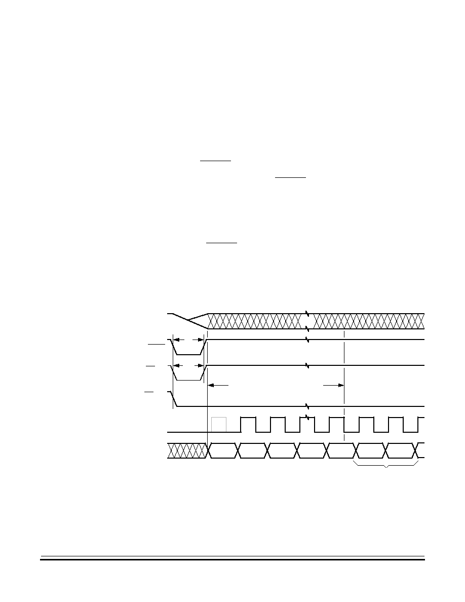
Low-Power Modes
Data-Retention Mode
MC68HC705KJ1 -- Rev. 2.0
Technical Data
MOTOROLA
Low-Power Modes
79
6.5 Data-Retention Mode
In data-retention mode, the MCU retains RAM contents and CPU
register contents at V
DD
voltages as low as 2.0 Vdc. The data-retention
feature allows the MCU to remain in a low power-consumption state
during which it retains data, but the CPU cannot execute instructions.
To put the MCU in data-retention mode:
1. Drive the RESET pin to logic 0.
2. Lower the V
DD
voltage. The RESET pin must remain low
continuously during data-retention mode.
To take the MCU out of data-retention mode:
1. Return V
DD
to normal operating voltage.
2. Return the RESET pin to logic 1.
6.6 Timing
Figure 6-1. Stop Mode Recovery Timing
t
ILIH
OSCILLATOR STABILIZATION DELAY
(5)
OSC
t
RL
RESET
IRQ/V
PP
IRQ/V
PP
INTERNAL
CLOCK
INTERNAL
ADDRESS
Notes:
1. Internal clocking from OSC1 pin
2. Edge-triggered external interrupt mask option
3. Edge- and level-triggered external interrupt mask option
4. Reset vector shown as example
RESET OR INTERRUPT
VECTOR FETCH
$07FE
$07FE
$07FE
$07FE
$07FE
$07FF
(NOTE 4)
BUS
(NOTE 3)
(NOTE 2)
(NOTE 1)
5. 4064 cycles or 128 cycles, depending on state of SOSCD bit in MOR
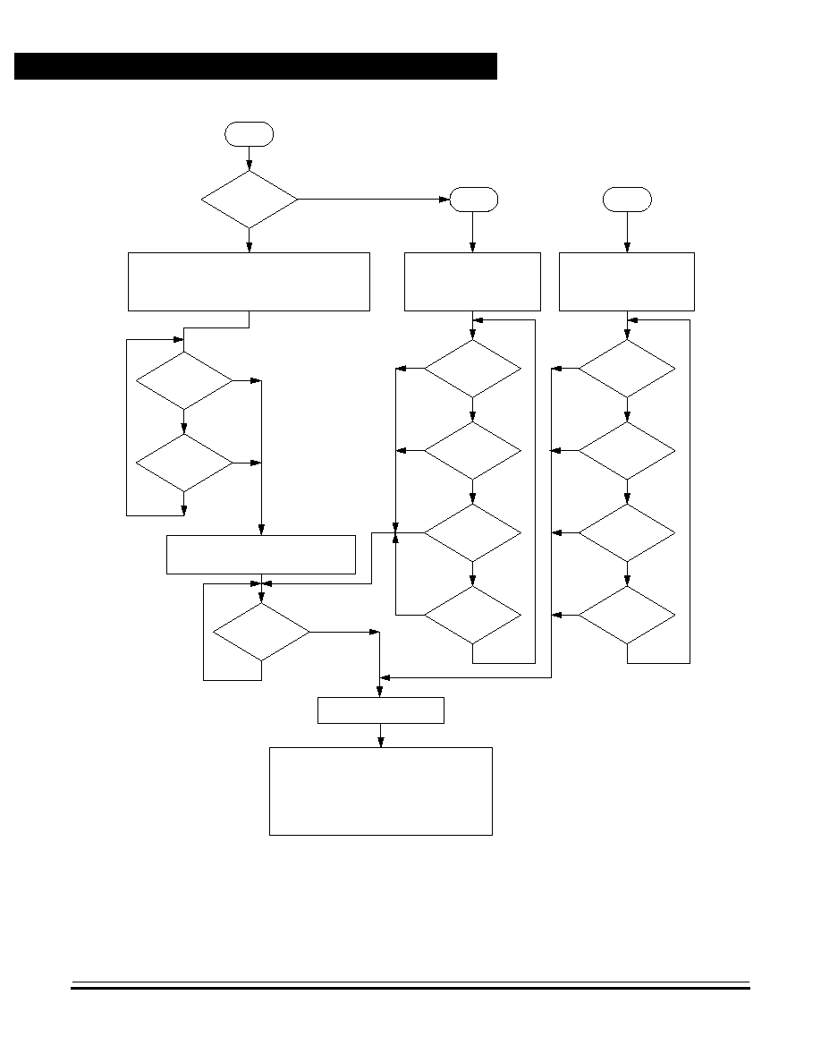
Technical Data
MC68HC705KJ1 -- Rev. 2.0
80
Low-Power Modes
MOTOROLA
Low-Power Modes
Figure 6-2. STOP/HALT/WAIT Flowchart
STOP
SWAIT
BIT SET?
CLEAR I BIT IN CCR.
SET IRQE BIT IN ISCR.
CLEAR TOF, RTIF, TOIE, AND RTIE BITS IN TSCR.
TURN OFF INTERNAL OSCILLATOR.
EXTERNAL
RESET?
EXTERNAL
INTERRUPT?
NO
NO
NO
TURN ON INTERNAL OSCILLATOR.
RESET STABILIZATION TIMER.
YES
YES
HALT
YES
END OF
STABILIZATION
DELAY?
YES
NO
YES
NO
NO
NO
COP
RESET?
TIMER
INTERRUPT?
EXTERNAL
INTERRUPT?
EXTERNAL
RESET?
CLEAR I BIT IN CCR.
SET IRQE BIT IN ISCR.
TURN OFF CPU CLOCK.
TIMER CLOCK ACTIVE.
YES
YES
YES
YES
NO
NO
NO
CLEAR I BIT IN CCR.
SET IRQE BIT IN ISCR.
TURN OFF CPU CLOCK.
TIMER CLOCK ACTIVE.
YES
YES
YES
NO
NO
TURN ON CPU CLOCK.
1. LOAD PC WITH RESET VECTOR
OR
2. SERVICE INTERRUPT.
a. SAVE CPU REGISTERS ON STACK.
b. SET I BIT IN CCR.
c. LOAD PC WITH INTERRUPT VECTOR.
EXTERNAL
RESET?
WAIT
EXTERNAL
INTERRUPT?
TIMER
INTERRUPT?
COP
RESET?

MC68HC705KJ1 -- Rev. 2.0
Technical Data
MOTOROLA
Parallel I/O Ports
81
Technical Data -- MC68HC705KJ1
Section 7. Parallel I/O Ports
7.1 Contents
7.2
Introduction . . . . . . . . . . . . . . . . . . . . . . . . . . . . . . . . . . . . . . . .81
7.3
Port A . . . . . . . . . . . . . . . . . . . . . . . . . . . . . . . . . . . . . . . . . . . .83
7.3.1
Port A Data Register . . . . . . . . . . . . . . . . . . . . . . . . . . . . . .83
7.3.2
Data Direction Register A . . . . . . . . . . . . . . . . . . . . . . . . . . .83
7.3.3
Pulldown Register A . . . . . . . . . . . . . . . . . . . . . . . . . . . . . . .85
7.3.4
Port LED Drive Capability. . . . . . . . . . . . . . . . . . . . . . . . . . .85
7.3.5
Port A I/O Pin Interrupts . . . . . . . . . . . . . . . . . . . . . . . . . . . .86
7.4
Port B . . . . . . . . . . . . . . . . . . . . . . . . . . . . . . . . . . . . . . . . . . . .86
7.4.1
Port B Data Register . . . . . . . . . . . . . . . . . . . . . . . . . . . . . .86
7.4.2
Data Direction Register B . . . . . . . . . . . . . . . . . . . . . . . . . . .87
7.4.3
Pulldown Register B . . . . . . . . . . . . . . . . . . . . . . . . . . . . . . .89
7.5
I/O Port Electrical Characteristics . . . . . . . . . . . . . . . . . . . . . . .90
7.2 Introduction
Ten bidirectional pins form one 8-bit input/output (I/O) port and one 2-bit
I/O port. All the bidirectional port pins are programmable as inputs or
outputs.
NOTE:
Connect any unused I/O pins to an appropriate logic level, either V
DD
or
V
SS
. Although the I/O ports do not require termination for proper
operation, termination reduces excess current consumption and the
possibility of electrostatic damage.
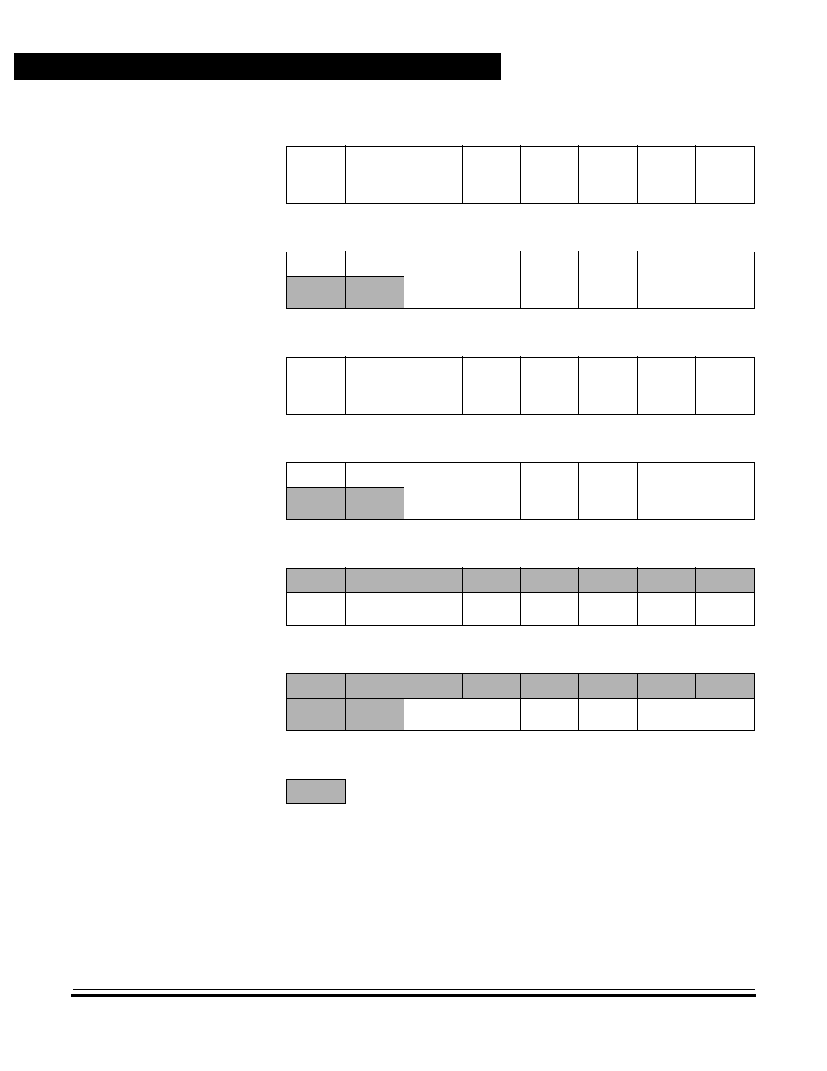
Technical Data
MC68HC705KJ1 -- Rev. 2.0
82
Parallel I/O Ports
MOTOROLA
Parallel I/O Ports
Addr.
Register Name:
Bit 7
6
5
4
3
2
1
Bit 0
$0000
Port A Data Register
(PORTA)
See page 83.
Read:
PA7
PA6
PA5
PA4
PA3
PA2
PA1
PA0
Write:
Reset:
Unaffected by reset
$0001
Port B Data Register
(PORTB)
See page 86.
Read:
0
0
See Note
PB3
PB2
See Note
Write:
Reset:
Unaffected by reset
$0004
Data Direction Register A
(DDRA)
See page 83.
Read:
DDRA7
DDRA6
DDRA5
DDRA4
DDRA3
DDRA2
DDRA1
DDRA0
Write:
Reset:
0
0
0
0
0
0
0
0
$0005
Data Direction Register B
(DDRB)
See page 87.
Read:
0
0
See Note
DDRB3
DDRB2
See Note
Write:
Reset:
0
0
0
0
0
0
0
0
$0010
Port A Pulldown Register
(PDRA)
See page 85.
Read:
Write:
PDIA7
PDIA6
PDIA5
PDIA4
PDIA3
PDIA2
PDIA1
PDIA0
Reset:
0
0
0
0
0
0
0
0
$0011
Port B Pulldown Register
(PDRB)
See page 89.
Read:
Write:
See Note
PDIB3
PDIB2
See Note
Reset:
0
0
0
0
0
0
= Unimplemented
Note:
PB5, PB4, PB1, and PB0 should be configured as inputs at all times. These bits are available for read/write but are not available exter-
nally. Configuring them as inputs will ensure that the pulldown devices are enabled, thus properly terminating them.
Figure 7-1. Parallel I/O Port Register Summary
Parallel I/O Ports
Port A
MC68HC705KJ1 -- Rev. 2.0
Technical Data
MOTOROLA
Parallel I/O Ports
83
7.3 Port A
Port A is an 8-bit bidirectional port.
7.3.1 Port A Data Register
The port A data register contains a latch for each port A pin.
PA[7:0] -- Port A Data Bits
These read/write bits are software programmable. Data direction of
each port A pin is under the control of the corresponding bit in data
direction register A. Reset has no effect on port A data.
7.3.2 Data Direction Register A
Data direction register A determines whether each port A pin is an input
or an output.
Address:
$0000
Bit 7
6
5
4
3
2
1
Bit 0
Read:
PA7
PA6
PA5
PA4
PA3
PA2
PA1
PA0
Write:
Reset:
Unaffected by reset
Figure 7-2. Port A Data Register (PORTA)
Address:
$0004
Bit 7
6
5
4
3
2
1
Bit 0
Read:
DDRA7
DDRA6
DDRA5
DDRA4
DDRA3
DDRA2
DDRA1
DDRA0
Write:
Reset:
0
0
0
0
0
0
0
0
Figure 7-3. Data Direction Register A (DDRA)
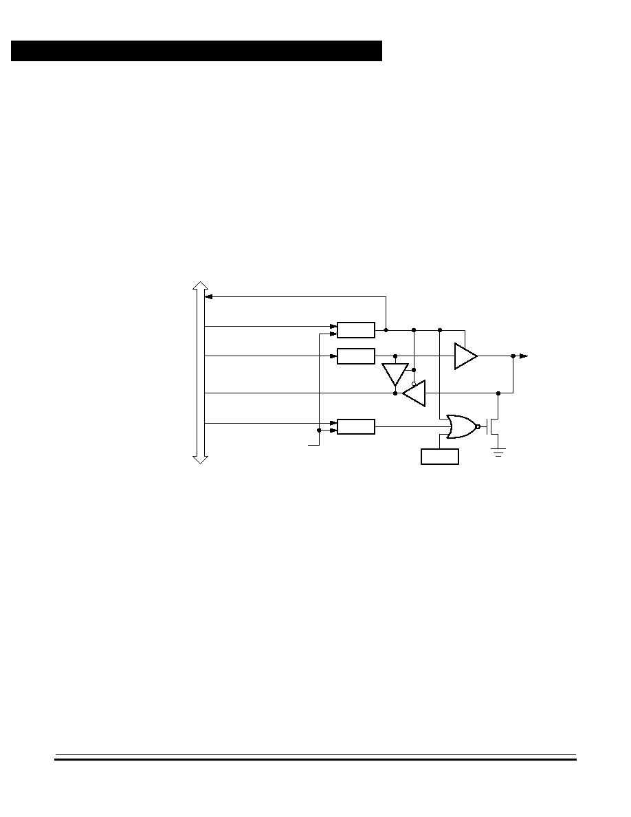
Technical Data
MC68HC705KJ1 -- Rev. 2.0
84
Parallel I/O Ports
MOTOROLA
Parallel I/O Ports
DDRA[7:0] -- Data Direction Register A Bits
These read/write bits control port A data direction. Reset clears
DDRA[7:0], configuring all port A pins as inputs.
1 = Corresponding port A pin configured as output
0 = Corresponding port A pin configured as input
NOTE:
Avoid glitches on port A pins by writing to the port A data register before
changing data direction register A bits from 0 to 1.
Figure 7-4
shows the I/O logic of port A.
Figure 7-4. Port A I/O Circuitry
Writing a logic 1 to a DDRA bit enables the output buffer for the
corresponding port A pin; a logic 0 disables the output buffer.
When bit DDRAx is a logic 1, reading address $0000 reads the PAx data
latch. When bit DDRAx is a logic 0, reading address $0000 reads the
voltage level on the pin. The data latch can always be written, regardless
of the state of its data direction bit.
Table 7-1
summarizes the operation
of the port A pins.
READ DDRA
WRITE DDRA
RESET
WRITE PORTA
READ PORTA
PAx
INTERNAL D
A
T
A
B
U
S
DDRAx
PAx
PDRAx
SWPDI
100-
µ
A
PULLDOWN
(PA0≠PA3 TO
IRQ MODULE)
WRITE PDRA
10-mA SINK CAPABILITY
(PINS PA4≠PA7 ONLY)
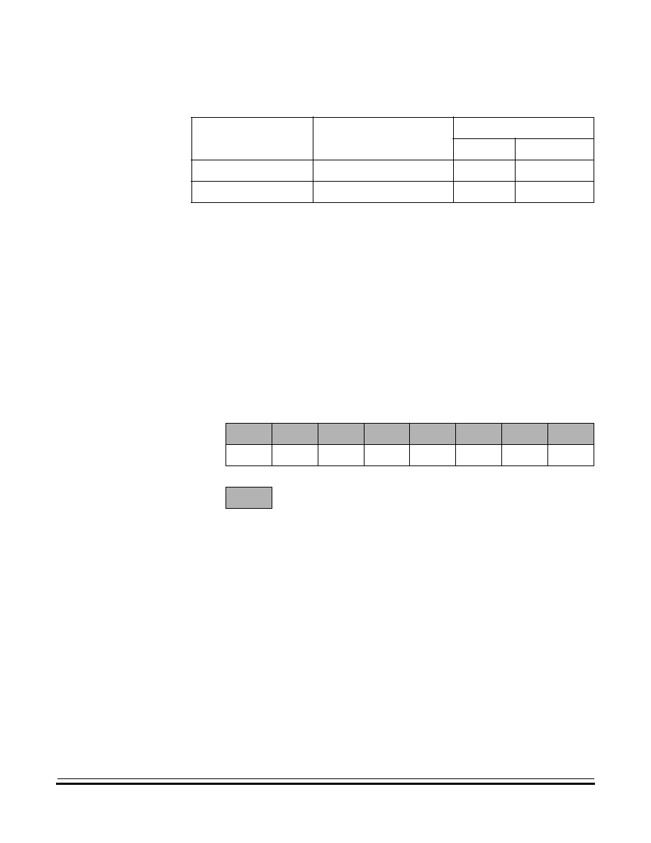
Parallel I/O Ports
Port A
MC68HC705KJ1 -- Rev. 2.0
Technical Data
MOTOROLA
Parallel I/O Ports
85
7.3.3 Pulldown Register A
Pulldown register A inhibits the pulldown devices on port A pins
programmed as inputs.
NOTE:
If the SWPDI bit in the mask option register is programmed to logic 1,
reset initializes all port A pins as inputs with disabled pulldown devices.
PDIA[7:0] -- Pulldown Inhibit A Bits
PDIA[7:0] disable the port A pulldown devices. Reset clears
PDIA[7:0].
1 = Corresponding port A pulldown device disabled
0 = Corresponding port A pulldown device not disabled
7.3.4 Port LED Drive Capability
All outputs can drive light-emitting diodes (LEDs). These pins can sink
approximately 10 mA of current to V
SS
.
Table 7-1. Port A Pin Operation
Data Direction Bit
I/O Pin Mode
Accesses to Data Bit
Read
Write
0
Input, high-impedance
Pin
Latch
(1)
1. Writing affects the data register but does not affect input.
1
Output
Latch
Latch
Address:
$0010
Bit 7
6
5
4
3
2
1
Bit 0
Read:
Write:
PDIA7
PDIA6
PDIA5
PDIA4
PDIA3
PDIA2
PDIA1
PDIA0
Reset:
0
0
0
0
0
0
0
0
= Unimplemented
Figure 7-5. Pulldown Register A (PDRA)
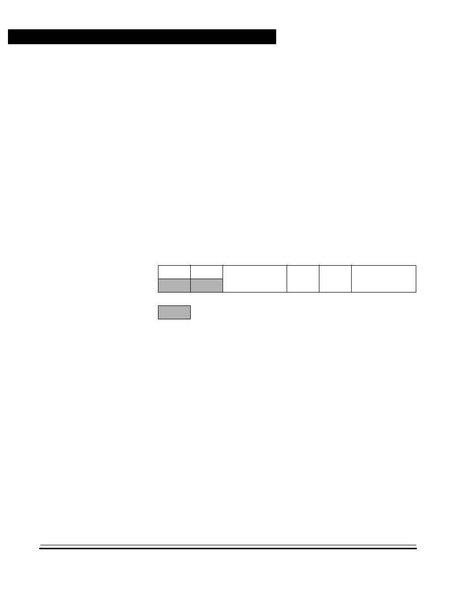
Technical Data
MC68HC705KJ1 -- Rev. 2.0
86
Parallel I/O Ports
MOTOROLA
Parallel I/O Ports
7.3.5 Port A I/O Pin Interrupts
If the PIRQ bit in the mask option register is programmed to logic 1,
PA0≠PA3 pins function as external interrupt pins. (See
Section 9.
External Interrupt Module (IRQ)
.)
7.4 Port B
Port B is a 2-bit bidirectional port.
7.4.1 Port B Data Register
The port B data register contains a latch for each port B pin.
PB[3:2] -- Port B Data Bits
These read/write bits are software programmable. Data direction of each
port B pin is under the control of the corresponding bit in data direction
register B. Reset has no effect on port B data.
NOTE:
PB4≠PB5 and PB0≠PB1 should be configured as inputs at all times.
These bits are available for read/write but are not available externally.
Configuring them as inputs will ensure that the pulldown devices are
enabled, thus properly terminating them.
Address:
$0001
Bit 7
6
5
4
3
2
1
Bit 0
Read:
0
0
See Note
PB3
PB2
See Note
Write:
Reset:
Unaffected by reset
= Unimplemented
Note:
PB5, PB4, PB1, and PB0 should be configured as inputs at all times. These bits are available for
read/write but are not available externally. Configuring them as inputs will ensure that the pulldown
devices are enabled, thus properly terminating them.
Figure 7-6. Port B Data Register (PORTB)

Parallel I/O Ports
Port B
MC68HC705KJ1 -- Rev. 2.0
Technical Data
MOTOROLA
Parallel I/O Ports
87
7.4.2 Data Direction Register B
Data direction register B determines whether each port B pin is an input
or an output.
DDRB[3:2] -- Data Direction Register B Bits
These read/write bits control port B data direction. Reset clears
DDRB[3:2], configuring all port B pins as inputs.
1 = Corresponding port B pin configured as output
0 = Corresponding port B pin configured as input
NOTE:
Avoid glitches on port B pins by writing to the port B data register before
changing data direction register B bits from 0 to 1.
Figure 7-8
shows the I/O logic of port B.
Address:
$0005
Bit 7
6
5
4
3
2
1
Bit 0
Read:
0
0
See Notes
DDRB3
DDRB2
See Note
Write:
Reset:
0
0
0
0
0
0
0
0
= Unimplemented
Note:
DDRB5, DDRB4, DDRB1, and DDRB0 should be configured as inputs at all times. These bits are
available for read/write but are not available externally. Configuring them as inputs will ensure that the
pulldown devices are enabled, thus properly terminating them.
Figure 7-7. Data Direction Register B (DDRB)
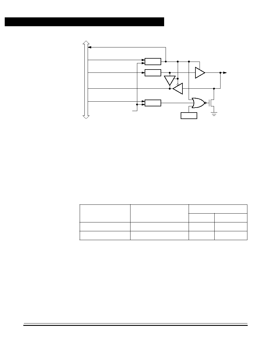
Technical Data
MC68HC705KJ1 -- Rev. 2.0
88
Parallel I/O Ports
MOTOROLA
Parallel I/O Ports
Figure 7-8. Port B I/O Circuitry
Writing a logic 1 to a DDRB bit enables the output buffer for the
corresponding port B pin; a logic 0 disables the output buffer.
When bit DDRBx is a logic 1, reading address $0001 reads the PBx data
latch. When bit DDRBx is a logic 0, reading address $0001 reads the
voltage level on the pin. The data latch can always be written, regardless
of the state of its data direction bit.
Table 7-2
summarizes the operation
of the port B pins.
Table 7-2. Port B Pin Operation
Data Direction Bit
I/O Pin Mode
Accesses to Data Bit
Read
Write
0
Input, high-impedance
Pin
Latch
(1)
1. Writing affects the data register, but does not affect input.
1
Output
Latch
Latch
READ DDRB
WRITE DDRB
RESET
WRITE PORTB
READ PORTB
PBx
INTERNAL D
A
T
A
B
U
S
DDRBx
PBx
PDRBx
SWPDI
100-
µ
A
PULLDOWN
WRITE PDRB
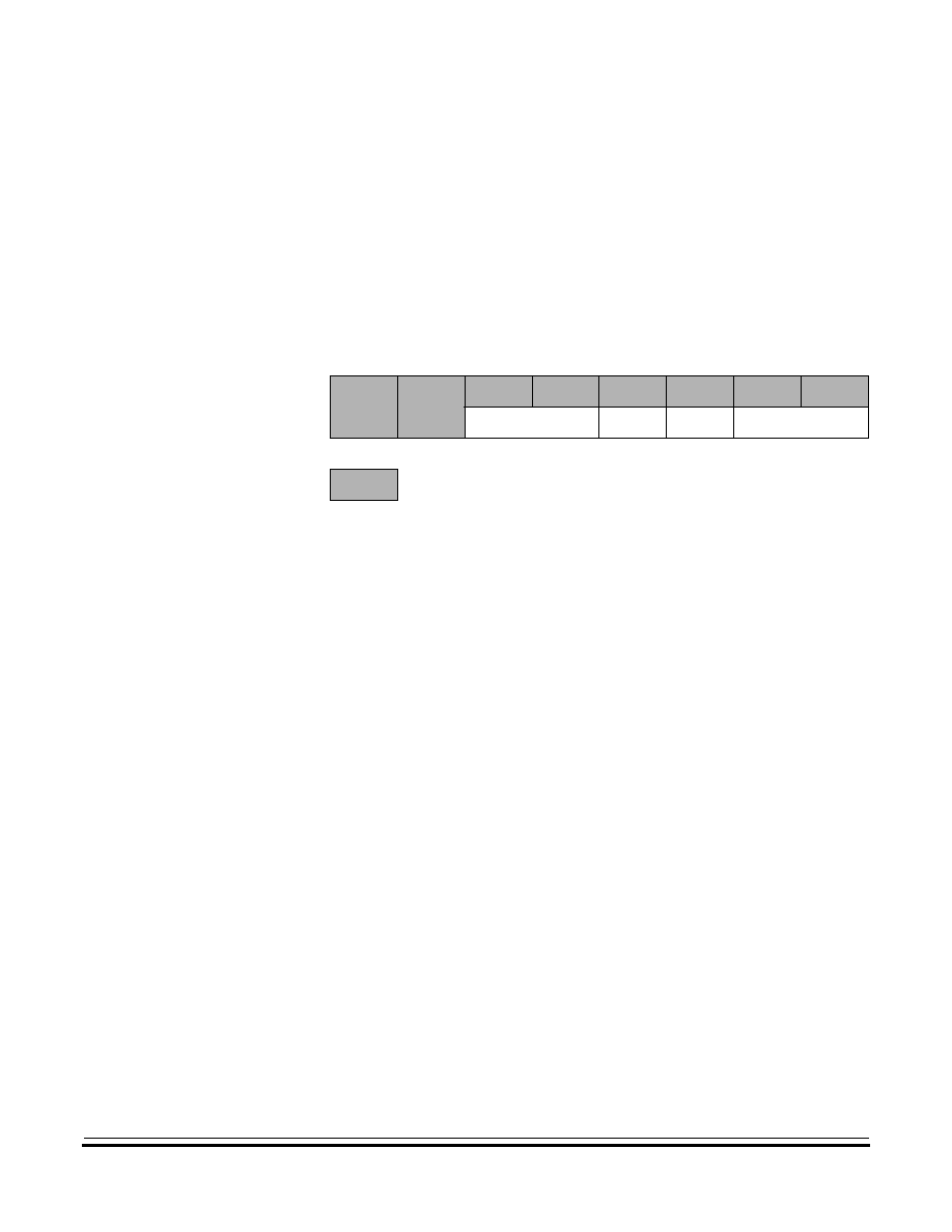
Parallel I/O Ports
Port B
MC68HC705KJ1 -- Rev. 2.0
Technical Data
MOTOROLA
Parallel I/O Ports
89
7.4.3 Pulldown Register B
Pulldown register B inhibits the pulldown devices on port B pins
programmed as inputs.
NOTE:
If the SWPDI bit in the mask option register is programmed to logic 1,
reset initializes all port B pins as inputs with disabled pulldown devices.
PDIB[3:2] -- Pulldown Inhibit B Bits
PDIB[3:2] disable the port B pulldown devices. Reset clears
PDIB[3:2].
1 = Corresponding port B pulldown device disabled
0 = Corresponding port B pulldown device not disabled
Address:
$0011
Bit 7
6
5
4
3
2
1
Bit 0
Read:
Write:
See Note
PDIB3
PDIB2
See Note
Reset:
0
0
0
0
0
0
= Unimplemented
Note:
These pulldown devices are permanently enabled when PB5, PB4, PB1 and PB0 are configured as
inputs.
Figure 7-9. Pulldown Register B (PDRB)

Technical Data
MC68HC705KJ1 -- Rev. 2.0
90
Parallel I/O Ports
MOTOROLA
Parallel I/O Ports
7.5 I/O Port Electrical Characteristics
Table 7-3. I/O Port DC Electrical Characteristics (V
DD
= 5.0 V)
(1)
1. V
DD
= 5.0 Vdc
±
10%, V
SS
= 0 Vdc, T
A
= ≠40
∞
C to +85
∞
C, unless otherwise noted.
Characteristic
Symbol
Min
Typ
(2)
2. Typical values reflect average measurements at midpoint of voltage range, 25
∞
C.
Max
Unit
Current Drain Per Pin
I
--
--
25
mA
Output High Voltage
(I
Load
=
≠
2.5 mA) PA4≠PA7
(I
Load
= ≠5.5 mA) PB2≠PB3, PA0≠PA3
V
OH
V
DD
≠0.8
V
DD
≠0.8
--
--
--
--
V
Output Low Voltage
(I
Load
= 10.0 mA) PA0≠PA7, PB2≠PB3
V
OL
--
--
0.8
V
Input High Voltage
PA0≠PA7, PB2≠PB3
V
IH
0.7 x V
DD
--
V
DD
V
Input Low Voltage
PA0≠PA7, PB2≠PB3
V
IL
V
SS
--
0.2 x V
DD
V
I/O Ports Hi-Z Leakage Current
PA0≠PA7, PB2≠PB3 (Without Individual
Pulldown Activated)
I
IL
--
0.2
±
1
µ
A
Input Pulldown Current
PA0≠PA7, PB2≠PB3 (With Individual
Pulldown Activated)
I
IL
35
80
200
µ
A

Parallel I/O Ports
I/O Port Electrical Characteristics
MC68HC705KJ1 -- Rev. 2.0
Technical Data
MOTOROLA
Parallel I/O Ports
91
Table 7-4. I/O Port DC Electrical Characteristics (V
DD
= 3.3 V)
(1)
Characteristic
Symbol
Min
Typ
(2)
Max
Unit
Current Drain Per Pin
I
--
--
25
mA
Output High Voltage
(I
Load
=
≠
0.8 mA) PA4≠PA7
(I
Load
=
≠
1.5 mA) PA0≠PA3, PB2≠PB3
V
OH
V
DD
≠0.3
V
DD
≠0.3
--
--
--
--
V
Output Low Voltage
(I
Load
= 5.0 mA) PA4≠PA7
(I
Load
= 3.5 mA) PA0≠PA3, PB2≠PB3
V
OL
--
--
--
--
0.5
0.5
V
Input High Voltage
PA0≠PA7, PB2≠PB3
V
IH
0.7 x V
DD
--
V
DD
V
Input Low Voltage
PA0≠PA7, PB2≠PB3
V
IL
V
SS
--
0.2 x V
DD
V
I/O Ports Hi-Z Leakage Current
PA0≠PA7, PB2≠PB3 (Without Individual Pulldown
Activated)
I
IL
--
0.1
±
1
µ
A
Input Pulldown Current
PA0≠PA7, PB2≠PB3 (With Individual Pulldown
Activated)
I
IL
12
30
100
µ
A
1. V
DD
= 3.3 Vdc
±
10%, V
SS
= 0 Vdc, T
A
= ≠40
∞
C to +85
∞
C, unless otherwise noted.
2. Typical values reflect average measurements at midpoint of voltage range, 25
∞
C.

Technical Data
MC68HC705KJ1 -- Rev. 2.0
92
Parallel I/O Ports
MOTOROLA
Parallel I/O Ports

MC68HC705KJ1 -- Rev. 2.0
Technical Data
MOTOROLA
Computer Operating Properly Module (COP)
93
Technical Data -- MC68HC705KJ1
Section 8. Computer Operating Properly Module (COP)
8.1 Contents
8.2
Introduction . . . . . . . . . . . . . . . . . . . . . . . . . . . . . . . . . . . . . . . .93
8.3
Features . . . . . . . . . . . . . . . . . . . . . . . . . . . . . . . . . . . . . . . . . .93
8.4
Operation . . . . . . . . . . . . . . . . . . . . . . . . . . . . . . . . . . . . . . . . .94
8.4.1
COP Watchdog Timeout . . . . . . . . . . . . . . . . . . . . . . . . . . .94
8.4.2
COP Watchdog Timeout Period . . . . . . . . . . . . . . . . . . . . . .94
8.4.3
Clearing the COP Watchdog . . . . . . . . . . . . . . . . . . . . . . . .95
8.5
Interrupts. . . . . . . . . . . . . . . . . . . . . . . . . . . . . . . . . . . . . . . . . .95
8.6
COP Register . . . . . . . . . . . . . . . . . . . . . . . . . . . . . . . . . . . . . .95
8.7
Low-Power Modes . . . . . . . . . . . . . . . . . . . . . . . . . . . . . . . . . .96
8.7.1
Stop Mode . . . . . . . . . . . . . . . . . . . . . . . . . . . . . . . . . . . . . .96
8.7.2
Wait Mode . . . . . . . . . . . . . . . . . . . . . . . . . . . . . . . . . . . . . .96
8.2 Introduction
The computer operating properly (COP) watchdog resets the MCU in
case of software failure. Software that is operating properly periodically
services the COP watchdog and prevents COP reset. The COP
watchdog function is programmable by the COPEN bit in the mask
option register.
8.3 Features
The computer operating properly module (COP) includes these features:
∑
Protection from Runaway Software
∑
Wait Mode and Halt Mode Operations

Technical Data
MC68HC705KJ1 -- Rev. 2.0
94
Computer Operating Properly Module (COP)
MOTOROLA
Computer Operating Properly Module (COP)
8.4 Operation
Operation of the COP module is discussed here.
8.4.1 COP Watchdog Timeout
Four counter stages at the end of the timer make up the COP watchdog.
The COP resets the MCU if the timeout period occurs before the COP
watchdog timer is cleared by application software and the IRQ/V
PP
pin
voltage is between V
SS
and V
DD
. Periodically clearing the counter starts
a new timeout period and prevents COP reset. A COP watchdog timeout
indicates that the software is not executing instructions in the correct
sequence.
NOTE:
The internal clock drives the COP watchdog. Therefore, the COP
watchdog cannot generate a reset for errors that cause the internal clock
to stop.
The COP watchdog depends on a power supply voltage at or above a
minimum specification and is not guaranteed to protect against
brownout.
8.4.2 COP Watchdog Timeout Period
The COP watchdog timer function is implemented by dividing the output
of the real-time interrupt circuit (RTI) by eight. The RTI select bits in the
timer status and control register control RTI output, and the selected
output drives the COP watchdog. (See timer status and control register
in
Section 10. Multifunction Timer Module
.)
Note that the minimum COP timeout period is seven times the RTI
period. The COP is cleared asynchronously with the value in the RTI
divider; hence, the COP timeout period will vary between 7x and 8x the
RTI period.

Computer Operating Properly Module (COP)
Interrupts
MC68HC705KJ1 -- Rev. 2.0
Technical Data
MOTOROLA
Computer Operating Properly Module (COP)
95
8.4.3 Clearing the COP Watchdog
To clear the COP watchdog and prevent a COP reset, write a logic 0 to
bit 0 (COPC) of the COP register at location $07F0 (see
Figure 8-1
).
Clearing the COP bit disables the COP watchdog timer regardless of the
IRQ/V
PP
pin voltage.
If the main program executes within the COP timeout period, the clearing
routine should be executed only once. If the main program takes longer
than the COP timeout period, the clearing routine must be executed
more than once.
NOTE:
Place the clearing routine in the main program and not in an interrupt
routine. Clearing the COP watchdog in an interrupt routine might prevent
COP watchdog timeouts even though the main program is not operating
properly.
8.5 Interrupts
The COP watchdog does not generate interrupts.
8.6 COP Register
The COP register (COPR) is a write-only register that returns the
contents of EPROM location $07F0 when read.
COPC -- COP Clear Bit
This write-only bit resets the COP watchdog. Reading address $07F0
returns undefined results.
Address:
$07F0
Bit 7
6
5
4
3
2
1
Bit 0
Read:
Write:
COPC
Reset:
U
U
U
U
U
U
U
0
= Unimplemented
U = Unaffected
Figure 8-1. COP Register (COPR)

Technical Data
MC68HC705KJ1 -- Rev. 2.0
96
Computer Operating Properly Module (COP)
MOTOROLA
Computer Operating Properly Module (COP)
8.7 Low-Power Modes
The STOP and WAIT instructions have the following effects on the COP
watchdog.
8.7.1 Stop Mode
The STOP instruction clears the COP watchdog counter and disables
the clock to the COP watchdog.
NOTE:
To prevent the STOP instruction from disabling the COP watchdog,
program the stop-to-wait conversion bit (SWAIT) in the mask option
register to logic 1.
Upon exit from stop mode by external reset:
∑
The counter begins counting from $0000.
∑
The counter is cleared again after the oscillator stabilization delay
and begins counting from $0000 again.
Upon exit from stop mode by external interrupt:
∑
The counter begins counting from $0000.
∑
The counter is not cleared again after the oscillator stabilization
delay and continues counting throughout the oscillator
stabilization delay.
NOTE:
Immediately after exiting stop mode by external interrupt, service the
COP to ensure a full COP timeout period.
8.7.2 Wait Mode
The WAIT instruction has no effect on the COP watchdog.
NOTE:
To prevent a COP timeout during wait mode, exit wait mode periodically
to service the COP.

MC68HC705KJ1 -- Rev. 2.0
Technical Data
MOTOROLA
External Interrupt Module (IRQ)
97
Technical Data -- MC68HC705KJ1
Section 9. External Interrupt Module (IRQ)
9.1 Contents
9.2
Introduction . . . . . . . . . . . . . . . . . . . . . . . . . . . . . . . . . . . . . . . .97
9.3
Features . . . . . . . . . . . . . . . . . . . . . . . . . . . . . . . . . . . . . . . . . .97
9.4
Operation . . . . . . . . . . . . . . . . . . . . . . . . . . . . . . . . . . . . . . . . .98
9.4.1
IRQ/V
PP
Pin . . . . . . . . . . . . . . . . . . . . . . . . . . . . . . . . . . . .101
9.4.2
Optional External Interrupts . . . . . . . . . . . . . . . . . . . . . . . .101
9.5
IRQ Status and Control Register . . . . . . . . . . . . . . . . . . . . . .102
9.6
Timing . . . . . . . . . . . . . . . . . . . . . . . . . . . . . . . . . . . . . . . . . . .104
9.2 Introduction
The external interrupt (IRQ) module provides asynchronous external
interrupts to the CPU. The following sources can generate external
interrupts:
∑
IRQ/V
PP
pin
∑
PA0≠PA3 pins
9.3 Features
The external interrupt module (IRQ) includes these features:
∑
Dedicated External Interrupt Pin (IRQ/V
PP
)
∑
Selectable Interrupt on Four Input/Output (I/O) Pins (PA0≠PA3)
∑
Programmable Edge-Only or Edge- and Level-Interrupt Sensitivity

Technical Data
MC68HC705KJ1 -- Rev. 2.0
98
External Interrupt Module (IRQ)
MOTOROLA
External Interrupt Module (IRQ)
9.4 Operation
The interrupt request/programming voltage pin (IRQ/V
PP
) and port A
pins 0≠3 (PA0≠PA3) provide external interrupts. The PIRQ bit in the
mask option register (MOR) enables PA0≠PA3 as IRQ interrupt sources,
which are combined into a single OR'ing function to be latched by the
IRQ latch.
Figure 9-1
shows the structure of the IRQ module.
After completing its current instruction, the CPU tests the IRQ latch. If
the IRQ latch is set, the CPU
then tests the I bit in the condition code register and the IRQE bit in the
IRQ status and control register. If the I bit is clear and the IRQE bit is set,
the CPU then begins the interrupt sequence. This interrupt is serviced
by the interrupt service routine located at $07FA and $07FB.
The CPU clears the IRQ latch while it fetches the interrupt vector, so that
another external interrupt request can be latched during the interrupt
service routine. As soon as the I bit is cleared during the return from
interrupt, the CPU can recognize the new interrupt request.
Figure 9-3
shows the sequence of events caused by an interrupt.
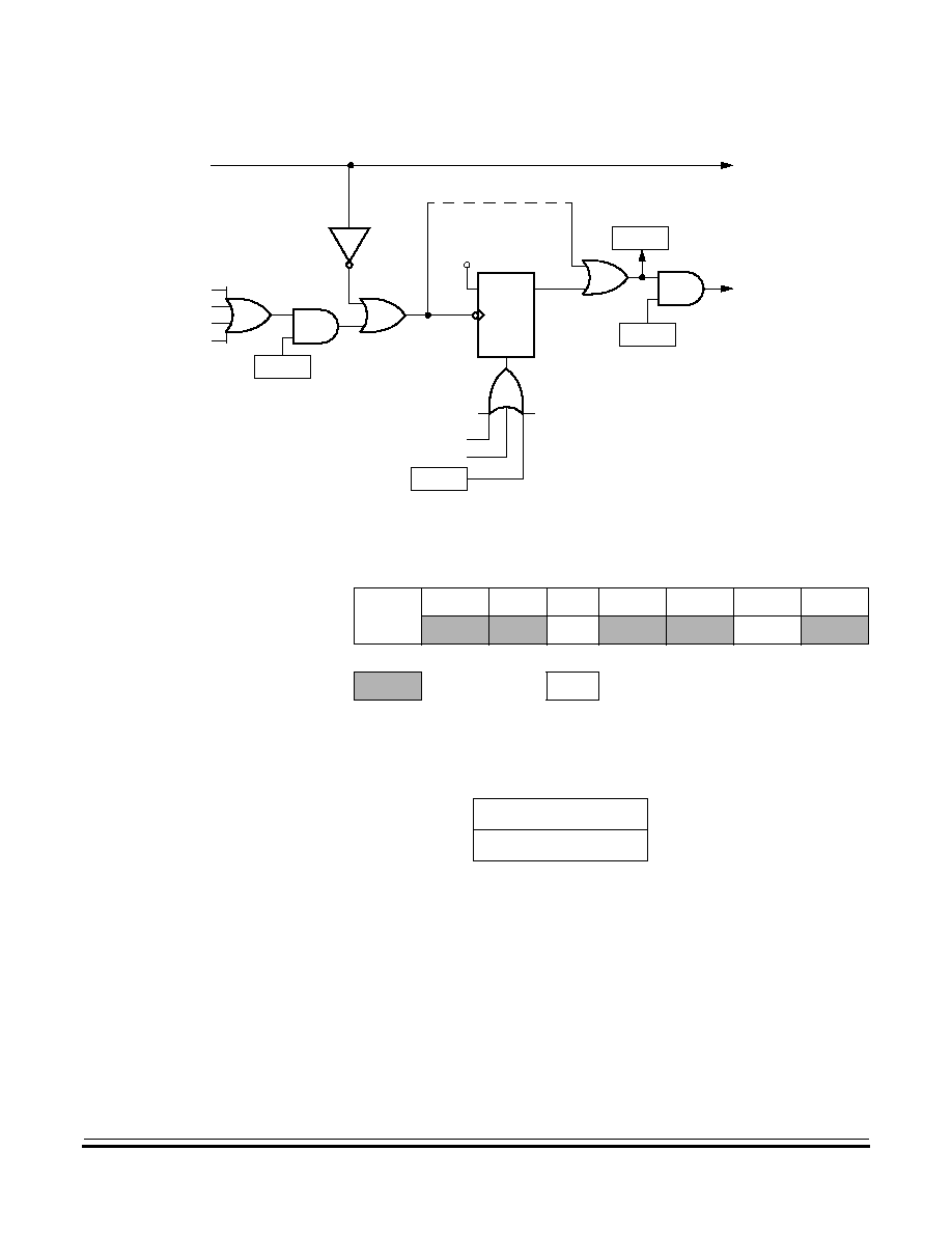
External Interrupt Module (IRQ)
Operation
MC68HC705KJ1 -- Rev. 2.0
Technical Data
MOTOROLA
External Interrupt Module (IRQ)
99
Figure 9-1. IRQ Module Block Diagram
Register Name
Bit 7
6
5
4
3
2
1
Bit 0
IRQ Status and Control
Register (ISCR)
See page 102.
Read:
IRQE
0
0
0
IRQF
0
0
0
Write:
R
IRQR
Reset:
1
0
0
0
0
0
0
0
= Unimplemented
R
= Reserved
Figure 9-2. IRQ Module I/O Register Summary
Table 9-1. I/O Register Address Summary
Register:
ISCR
Address:
$000A
PIRQ
LEVEL-SENSITIVE TRIGGER
PA3
PA2
PA1
IRQ
PA0
V
DD
(MOR LEVEL BIT)
RESET
IRQ VECTOR FETCH
EXTERNAL
INTERRUPT
REQUEST
(MOR)
TO BIH & BIL
INSTRUCTION
PROCESSING
IRQF
IRQR
IRQE
D
Q
CK
IRQ
CLR
LATCH
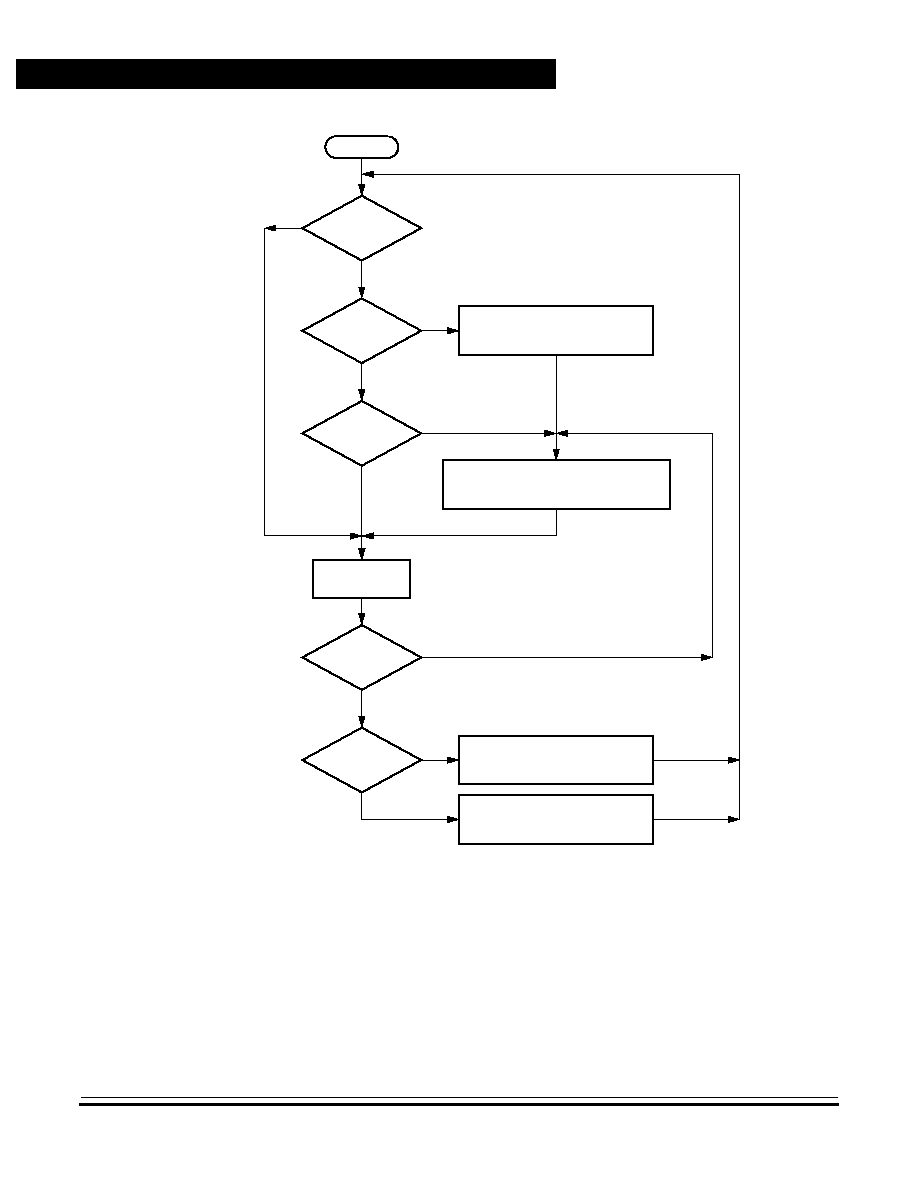
Technical Data
MC68HC705KJ1 -- Rev. 2.0
100
External Interrupt Module (IRQ)
MOTOROLA
External Interrupt Module (IRQ)
Figure 9-3. Interrupt Flowchart
EXTERNAL
INTERRUPT?
I BIT SET?
TIMER
INTERRUPT?
FETCH NEXT
INSTRUCTION.
SWI
INSTRUCTION?
RTI
INSTRUCTION?
STACK PCL, PCH, X, A, CCR.
SET I BIT.
LOAD PC WITH INTERRUPT VECTOR.
YES
YES
YES
YES
YES
UNSTACK CCR, A, X, PCH, PCL.
EXECUTE INSTRUCTION.
CLEAR IRQ LATCH.
NO
NO
NO
NO
NO
FROM RESET

External Interrupt Module (IRQ)
Operation
MC68HC705KJ1 -- Rev. 2.0
Technical Data
MOTOROLA
External Interrupt Module (IRQ)
101
9.4.1 IRQ/V
PP
Pin
An interrupt signal on the IRQ/V
PP
pin latches an external interrupt
request. The LEVEL bit in the mask option register provides negative
edge-sensitive triggering or both negative edge-sensitive and low
level-sensitive triggering for the interrupt function.
If edge- and level-sensitive triggering is selected, a falling edge or a low
level on the IRQ/V
PP
pin latches an external interrupt request. Edge- and
level-sensitive triggering allows the use of multiple wired-OR external
interrupt sources. An external interrupt request is latched as long as any
source is holding the IRQ/V
PP
pin low.
If level-sensitive triggering is selected, the IRQ/V
PP
input requires an
external resistor to V
DD
for wired-OR operation. If the IRQ/V
PP
pin is not
used, it must be tied to the V
DD
supply.
If edge-sensitive-only triggering is selected, a falling edge on the
IRQ/V
PP
pin latches an external interrupt request. A subsequent
external interrupt request can be latched only after the voltage level on
the IRQ/V
PP
pin returns to logic 1 and then falls again to logic 0.
The IRQ/V
PP
pin contains an internal Schmitt trigger as part of its input
to improve noise immunity. The voltage on this pin can affect the mode
of operation and should not exceed V
DD
.
9.4.2 Optional External Interrupts
The inputs for the lower four bits of port A (PA0≠PA3) can be connected
to the IRQ pin input of the CPU if enabled by the PIRQ bit in the mask
option register. This capability allows keyboard scan applications where
the transitions or levels on the I/O pins will behave the same as the
IRQ/V
PP
pin except for the inverted phase (logic 1, rising edge). The
active state of the IRQ/V
PP
pin is a logic 0 (falling edge).
The PA0≠PA3 pins are selected as a group to function as IRQ interrupts
and are enabled by the IRQE bit in the IRQ status and control register.
The PA0≠PA3 pins can be positive-edge triggered only or positive-edge
and high-level triggered.
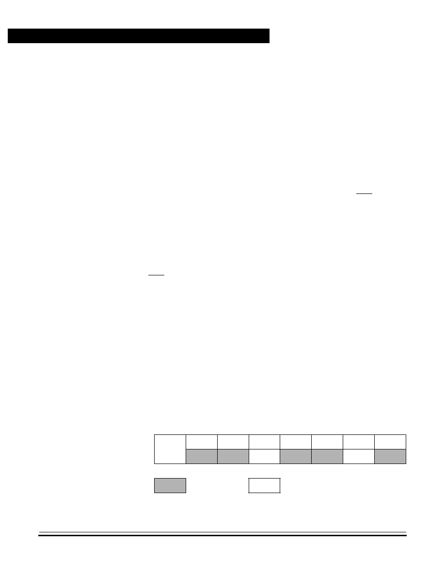
Technical Data
MC68HC705KJ1 -- Rev. 2.0
102
External Interrupt Module (IRQ)
MOTOROLA
External Interrupt Module (IRQ)
If edge- and level-sensitive triggering is selected, a rising edge or a high
level on a PA0≠PA3 pin latches an external interrupt request. Edge- and
level-sensitive triggering allows the use of multiple wired-OR external
interrupt sources. As long as any source is holding a PA0≠PA3 pin high,
an external interrupt request is latched, and the CPU continues to
execute the interrupt service routine.
If edge-sensitive only triggering is selected, a rising edge on a PA0≠PA3
pin latches an external interrupt request. A subsequent external interrupt
request can be latched only after the voltage level of the previous
interrupt signal returns to logic 0 and then rises again to logic 1.
NOTE:
The BIH and BIL instructions apply only to the level on the IRQ/V
PP
pin
itself and not to the output of the logic OR function with the PA0≠PA3
pins. The state of the individual port A pins can be checked by reading
the appropriate port A pins as inputs.
Enabled PA0≠PA3 pins cause an IRQ interrupt regardless of whether
these pins are configured as inputs or outputs.
The IRQ pin has an internal Schmitt trigger. The optional external
interrupts (PA0≠PA3) do not have internal Schmitt triggers.
The interrupt mask bit (I) in the condition code register (CCR) disables
all maskable interrupt requests, including external interrupt requests.
9.5 IRQ Status and Control Register
The IRQ status and control register (ISCR) controls and monitors
operation of the IRQ module. All unused bits in the ISCR read as logic
0s. The IRQF bit is cleared and the IRQE bit is set by reset.
Address:
$000A
Bit 7
6
5
4
3
2
1
Bit 0
Read:
IRQE
0
0
0
IRQF
0
0
0
Write:
R
IRQR
Reset:
1
0
0
0
0
0
0
0
= Unimplemented
R
= Reserved
Figure 9-4. IRQ Status and Control Register (ISCR)

External Interrupt Module (IRQ)
IRQ Status and Control Register
MC68HC705KJ1 -- Rev. 2.0
Technical Data
MOTOROLA
External Interrupt Module (IRQ)
103
IRQR -- Interrupt Request Reset Bit
This write-only bit clears the external interrupt request flag.
1 = Clears external interrupt and IRQF bit
0 = No effect on external interrupt and IRQF bit
IRQF -- External Interrupt Request Flag
The external interrupt request flag is a clearable, read-only bit that is
set when an external interrupt request is pending. Reset clears the
IRQF bit.
1 = External interrupt request pending
0 = No external interrupt request pending
IRQE -- External Interrupt Request Enable Bit
This read/write bit enables external interrupts. Reset sets the IRQE
bit.
1 = External interrupt requests enabled
0 = External interrupt requests disabled
The STOP and WAIT instructions set the IRQE bit so that an external
interrupt can bring the MCU out of these low-power modes. In addition,
reset sets the I bit which masks all interrupt sources.
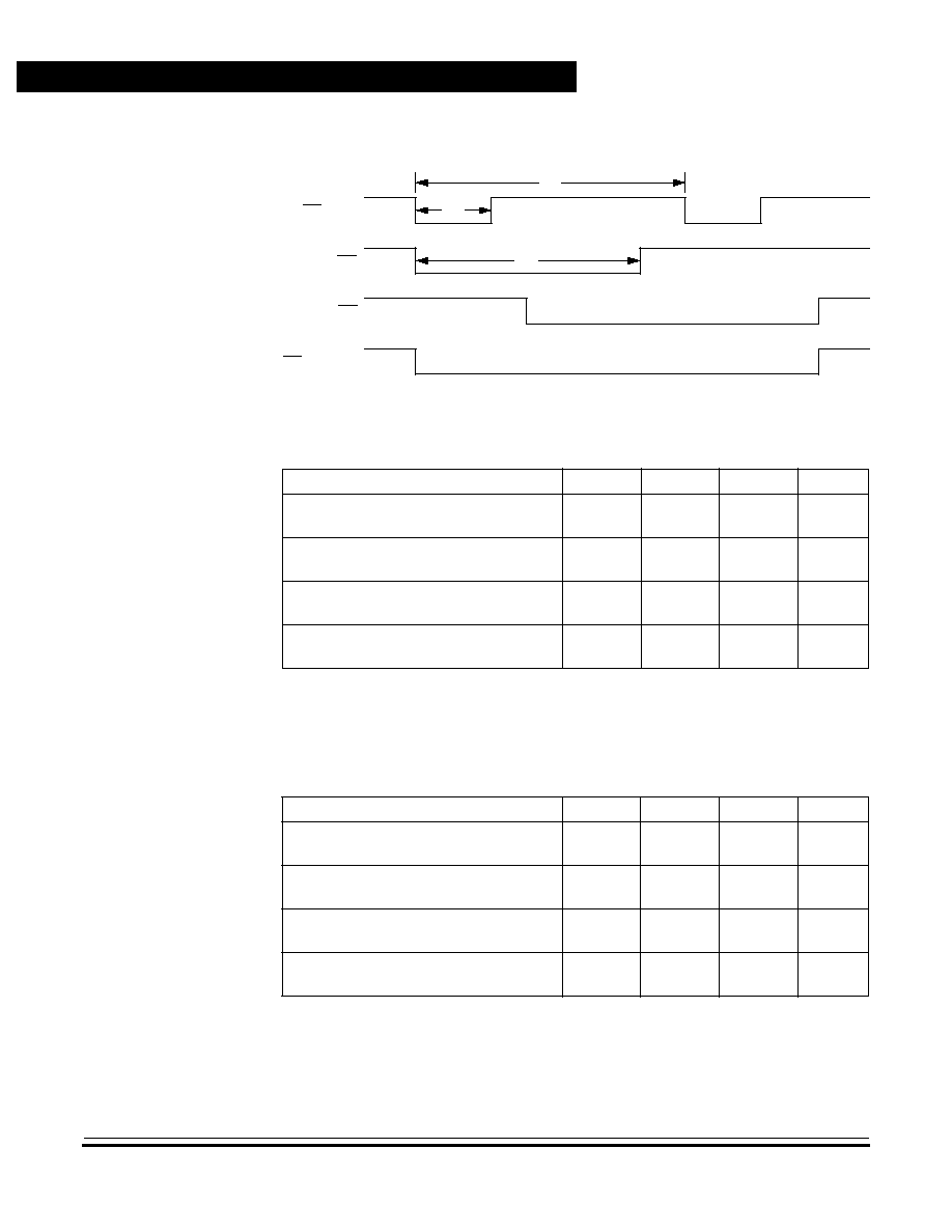
Technical Data
MC68HC705KJ1 -- Rev. 2.0
104
External Interrupt Module (IRQ)
MOTOROLA
External Interrupt Module (IRQ)
9.6 Timing
Figure 9-5. External Interrupt Timing
Table 9-2. External Interrupt Timing (V
DD
= 5.0 Vdc)
(1)
1. V
DD
= 5.0 Vdc
±
10%, V
SS
= 0 Vdc, T
A
= ≠40
∞
C to + 85
∞
C, unless otherwise noted.
Characteristic
Symbol
Min
Max
Unit
IRQ Interrupt Pulse Width Low
(Edge-Triggered)
t
ILIH
1.5
--
t
cyc
(2)
2.
t
cyc
= 1/f
OP
; f
OP
= f
OSC
/2.
IRQ Interrupt Pulse Width
(Edge- and Level-Triggered)
t
ILIH
1.5
Note
(3)
3. The minimum t
ILIL
should not be less than the number of interrupt service routine cycles
plus 19 t
cyc
.
t
cyc
PA0≠PA3 Interrupt Pulse Width High
(Edge-Triggered)
t
ILIL
1.5
--
t
cyc
PA0≠PA3 Interrupt Pulse Width High
(Edge- and Level-Triggered)
t
ILIH
1.5
Note
(3)
t
cyc
Table 9-3. External Interrupt Timing (V
DD
= 3.3 Vdc)
(1)
1. V
DD
= 3.3 Vdc
±
10%, V
SS
= 0 Vdc, T
A
= ≠40
∞
C to + 85
∞
C, unless otherwise noted.
Characteristic
Symbol
Min
Max
Unit
IRQ Interrupt Pulse Width Low
(Edge-Triggered)
t
ILIH
1.5
--
t
cyc
(2)
2.
t
cyc
= 1/f
OP
; f
OP
= f
OSC
/2.
IRQ Interrupt Pulse Width
(Edge- and Level-Triggered)
t
ILIH
1.5
Note
(3)
3. The minimum t
ILIL
should not be less than the number of interrupt service routine cycles
plus 19
t
cyc
.
t
cyc
PA0≠PA3 Interrupt Pulse Width High
(Edge-Triggered)
t
ILIL
1.5
--
t
cyc
PA0≠PA3 Interrupt Pulse Width High
(Edge- and Level-Triggered)
t
ILIH
1.5
Note
(3)
t
cyc
IRQ (INTERNAL)
t
ILIH
t
ILIL
t
ILIH
IRQ/V
PP
PIN
IRQ
1
IRQ
n
.
.
.

MC68HC705KJ1 -- Rev. 2.0
Technical Data
MOTOROLA
Multifunction Timer Module
105
Technical Data -- MC68HC705KJ1
Section 10. Multifunction Timer Module
10.1 Contents
10.2
Introduction . . . . . . . . . . . . . . . . . . . . . . . . . . . . . . . . . . . . . . .105
10.3
Features . . . . . . . . . . . . . . . . . . . . . . . . . . . . . . . . . . . . . . . . .105
10.4
Operation . . . . . . . . . . . . . . . . . . . . . . . . . . . . . . . . . . . . . . . .107
10.5
Interrupts. . . . . . . . . . . . . . . . . . . . . . . . . . . . . . . . . . . . . . . . .108
10.6
I/O Registers. . . . . . . . . . . . . . . . . . . . . . . . . . . . . . . . . . . . . .108
10.6.1
Timer Status and Control Register . . . . . . . . . . . . . . . . . . .108
10.6.2
Timer Counter Register . . . . . . . . . . . . . . . . . . . . . . . . . . .110
10.7
Low-Power Modes . . . . . . . . . . . . . . . . . . . . . . . . . . . . . . . . .111
10.7.1
Stop Mode . . . . . . . . . . . . . . . . . . . . . . . . . . . . . . . . . . . . .111
10.7.2
Wait Mode . . . . . . . . . . . . . . . . . . . . . . . . . . . . . . . . . . . . .111
10.2 Introduction
The multifunction timer provides a timing reference with programmable
real-time interrupt capability.
Figure 10-1
shows the timer organization.
10.3 Features
Features of the multifunction timer include:
∑
Timer Overflow
∑
Four Selectable Interrupt Rates
∑
Computer Operating Properly (COP) Watchdog Timer
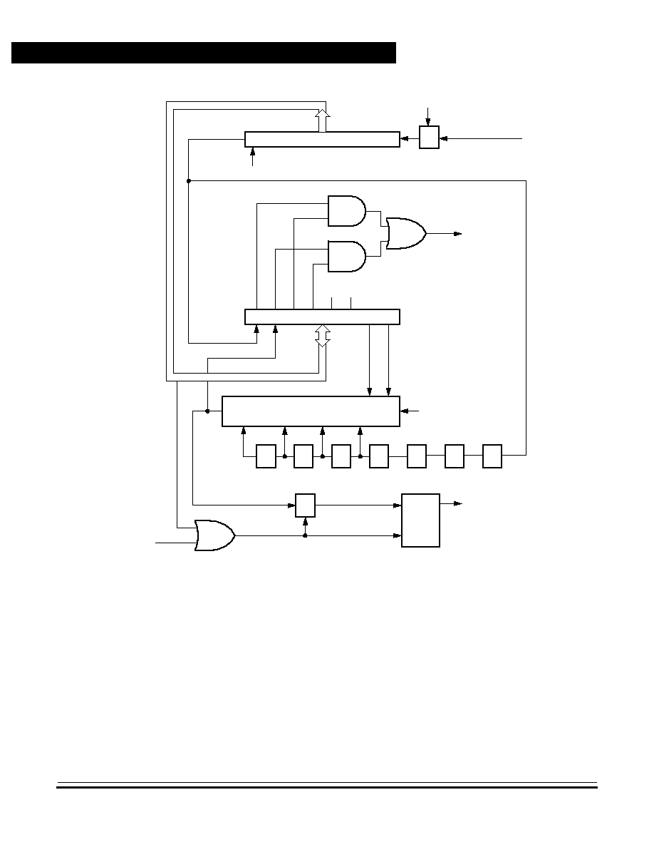
Technical Data
MC68HC705KJ1 -- Rev. 2.0
106
Multifunction Timer Module
MOTOROLA
Multifunction Timer Module
Figure 10-1. Multifunction Timer Block Diagram
CLEAR COP TIMER
TIMER COUNTER REGISTER
BITS [0:7] OF 15-STAGE
OVERFLOW
INTERNAL CLOCK
(XTAL
˜
2)
TIMER STATUS/CONTROL REGISTER
TO
F
R
TIF
T
OIE
R
TIE
T
OFR
R
TIFR
RT
1
RT
0
RTI RATE SELECT
˜
2
˜
2
˜
2
˜
2
˜
2
˜
2
˜
2
BITS [8:14] OF 15-STAGE RIPPLE COUNTER
˜
8
S
R
Q
INTERRUPT
REQUEST
COP RESET
INTERNAL D
A
T
A
B
U
S
RESET
RIPPLE COUNTER
RESET
RESET
RESET
˜
4
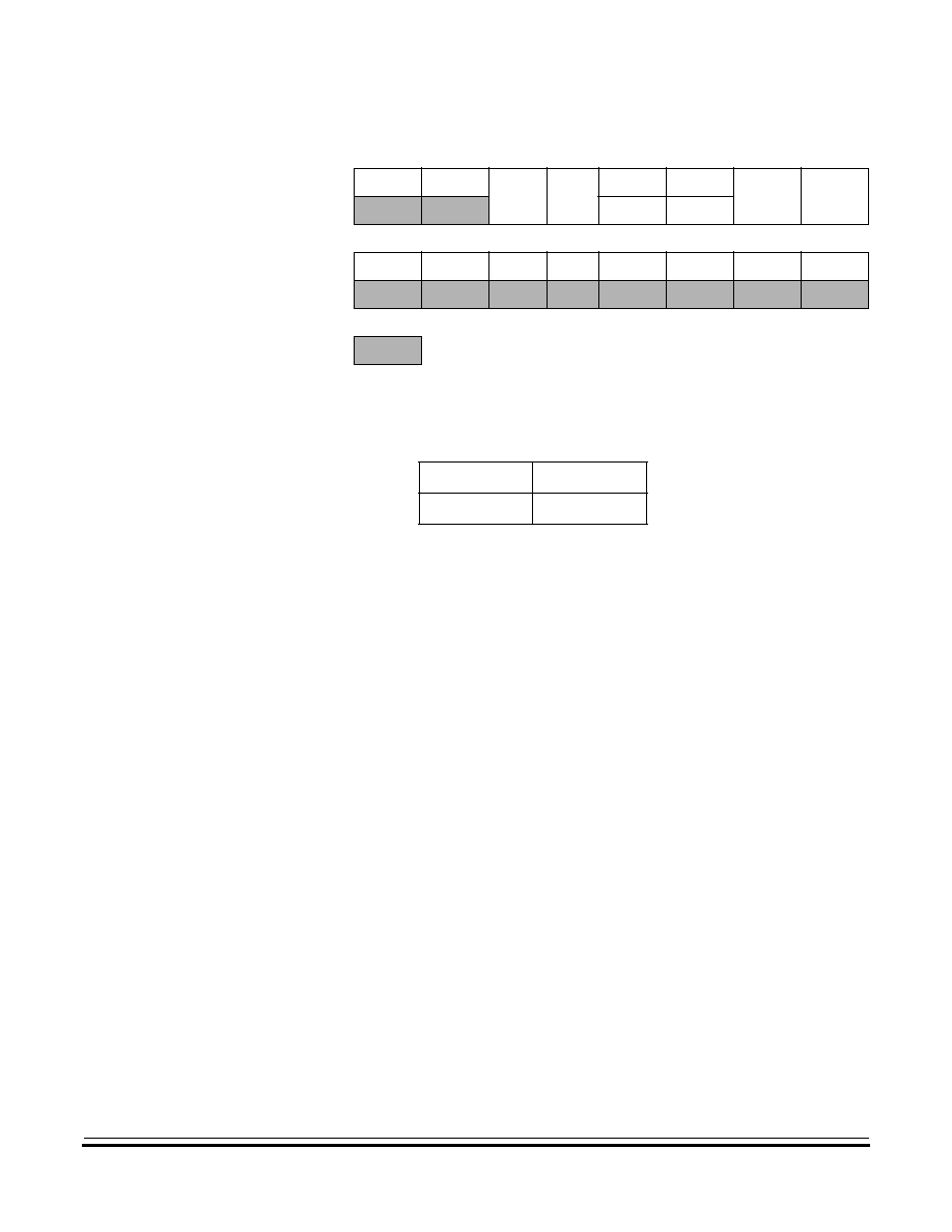
Multifunction Timer Module
Operation
MC68HC705KJ1 -- Rev. 2.0
Technical Data
MOTOROLA
Multifunction Timer Module
107
10.4 Operation
A 15-stage ripple counter, preceded by a prescaler that divides the
internal clock signal by four, provides the timing reference for the timer
functions. The value of the first eight timer stages can be read at any
time by accessing the timer counter register at address $0009. A timer
overflow function at the eighth stage allows a timer interrupt every 1024
internal clock cycles.
The next four stages lead to the real-time interrupt (RTI) circuit. The RT1
and RT0 bits in the timer status and control register at address $0008
allow a timer interrupt every 16,384, 32,768, 65,536, or 131,072 clock
cycles. The last four stages drive the selectable COP system. (For
information on the COP, refer to
Section 8. Computer Operating
Properly Module (COP)
.)
Register Name
Bit 7
6
5
4
3
2
1
Bit 0
Timer Status and Control Register
(TSCR)
See page 108.
Read:
TOF
RTIF
TOIE
RTIE
0
0
RT1
RT0
Write:
TOFR
RTIFR
Reset:
0
0
0
0
0
0
1
1
Timer Counter Register (TCR)
See page 110.
Read:
TMR7
TMR6
TMR5
TMR4
TMR3
TMR2
TMR1
TMR0
Write:
Reset:
0
0
0
0
0
0
0
0
= Unimplemented
Figure 10-2. I/O Register Summary
Table 10-1. I/O Register Address Summary
Register:
TSCR
TCR
Address:
$0008
$0009
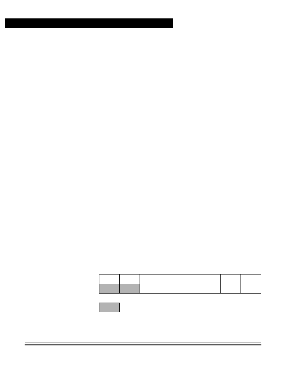
Technical Data
MC68HC705KJ1 -- Rev. 2.0
108
Multifunction Timer Module
MOTOROLA
Multifunction Timer Module
10.5 Interrupts
The following timer sources can generate interrupts:
∑
Timer overflow flag (TOF) -- The TOF bit is set when the first eight
stages of the counter roll over from $FF to $00. The timer overflow
interrupt enable bit, TOIE, enables TOF interrupt requests.
∑
Real-time interrupt flag (RTIF) -- The RTIF bit is set when the
selected RTI output becomes active. The real-time interrupt
enable bit, RTIE, enables RTIF interrupt requests.
10.6 I/O Registers
The following registers control and monitor the timer operation:
∑
Timer status and control register (TSCR)
∑
Timer counter register (TCR)
10.6.1 Timer Status and Control Register
The read/write timer status and control register performs the following
functions:
∑
Flags timer interrupts
∑
Enables timer interrupts
∑
Resets timer interrupt flags
∑
Selects real-time interrupt rates
Address:
$0008
Bit 7
6
5
4
3
2
1
Bit 0
Read:
TOF
RTIF
TOIE
RTIE
0
0
RT1
RT0
Write:
TOFR
RTIFR
Reset:
0
0
0
0
0
0
1
1
= Unimplemented
Figure 10-3. Timer Status and Control Register (TSCR)

Multifunction Timer Module
I/O Registers
MC68HC705KJ1 -- Rev. 2.0
Technical Data
MOTOROLA
Multifunction Timer Module
109
TOF -- Timer Overflow Flag
This read-only flag becomes set when the first eight stages of the
counter roll over from $FF to $00. TOF generates a timer overflow
interrupt request if TOIE is also set. Clear TOF by writing a logic 1 to
the TOFR bit. Writing to TOF has no effect. Reset clears TOF.
RTIF -- Real-Time Interrupt Flag
This read-only flag becomes set when the selected RTI output
becomes active. RTIF generates a real-time interrupt request if RTIE
is also set. Clear RTIF by writing a logic 1 to the RTIFR bit. Writing
to RTIF has no effect. Reset clears RTIF.
TOIE -- Timer Overflow Interrupt Enable Bit
This read/write bit enables timer overflow interrupts. Reset clears
TOIE.
1 = Timer overflow interrupts enabled
0 = Timer overflow interrupts disabled
RTIE -- Real-Time Interrupt Enable Bit
This read/write bit enables real-time interrupts. Reset clears RTIE.
1 = Real-time interrupts enabled
0 = Real-time interrupts disabled
TOFR -- Timer Overflow Flag Reset Bit
Writing a logic 1 to this write-only bit clears the TOF bit. TOFR always
reads as logic 0. Reset clears TOFR.
RTIFR -- Real-Time Interrupt Flag Reset Bit
Writing a logic 1 to this write-only bit clears the RTIF bit. RTIFR
always reads as logic 0. Reset clears RTIFR.
RT1 and RT0 -- Real-Time Interrupt Select Bits
These read/write bits select one of four real-time interrupt rates, as
shown in
Table 10-2
. Because the selected RTI output drives the
COP watchdog, changing the real-time interrupt rate also changes
the counting rate of the COP watchdog. Reset sets RT1 and RT0.
NOTE:
Changing RT1 and RT0 when a COP timeout is imminent can cause a
real-time interrupt request to be missed or an additional real-time
Technical Data
MC68HC705KJ1 -- Rev. 2.0
110
Multifunction Timer Module
MOTOROLA
Multifunction Timer Module
interrupt request to be generated. To prevent this occurrence, clear the
COP timer before changing RT1 and RT0.
10.6.2 Timer Counter Register
A 15-stage ripple counter is the core of the timer. The value of the first
eight stages is readable at any time from the read-only timer counter
register shown in
Figure 10-4
.
Power-on clears the entire counter chain and the internal clock begins
clocking the counter. After 4064 cycles (or 16 cycles if the SOSCD bit in
the mask option register is set), the power-on reset circuit is released,
clearing the counter again and allowing the MCU to come out of reset.
A timer overflow function at the eighth counter stage allows a timer
interrupt every 1024 internal clock cycles.
Table 10-2. Real-Time Interrupt Rate Selection
RT1:RT0
RTI
Rate
RTI Period
(f
OP
=
2 MHz)
COP Timeout
Period
(≠0/+1 RTI Period)
Minimum COP
Timeout Period
(f
OP
= 2 MHz)
0 0
f
OP
˜
2
14
8.2 ms
8 x RTI Period
65.5 ms
0 1
f
OP
˜
2
15
16.4 ms
8 x RTI Period
131.1 ms
1 0
f
OP
˜
2
16
32.8 ms
8 x RTI Period
262.1 ms
1 1
f
OP
˜
2
17
65.5 ms
8 x RTI Period
524.3 ms
Address:
$0009
Bit 7
6
5
4
3
2
1
Bit 0
Read:
TCR7
TCR6
TCR5
TCR4
TCR3
TCR2
TCR1
TCR0
Write:
Reset:
0
0
0
0
0
0
0
0
= Unimplemented
Figure 10-4. Timer Counter Register (TCR)

Multifunction Timer Module
Low-Power Modes
MC68HC705KJ1 -- Rev. 2.0
Technical Data
MOTOROLA
Multifunction Timer Module
111
10.7 Low-Power Modes
The STOP and WAIT instructions put the MCU in low
power-consumption standby states.
10.7.1 Stop Mode
The STOP instruction has the following effects on the timer:
∑
Clears the timer counter
∑
Clears interrupt flags (TOF and RTIF) and interrupt enable bits
(TOFE and RTIE) in TSCR, removing any pending timer interrupt
requests and disabling further timer interrupts
10.7.2 Wait Mode
The timer remains active after a WAIT instruction. Any enabled timer
interrupt request can bring the MCU out of wait mode.

Technical Data
MC68HC705KJ1 -- Rev. 2.0
112
Multifunction Timer Module
MOTOROLA
Multifunction Timer Module

MC68HC705KJ1 -- Rev. 2.0
Technical Data
MOTOROLA
Electrical Specifications
113
Technical Data -- MC68HC705KJ1
Section 11. Electrical Specifications
11.1 Contents
11.2
Maximum Ratings . . . . . . . . . . . . . . . . . . . . . . . . . . . . . . . . . .114
11.3
Operating Temperature Range. . . . . . . . . . . . . . . . . . . . . . . .115
11.4
Thermal Characteristics . . . . . . . . . . . . . . . . . . . . . . . . . . . . .115
11.5
Power Considerations. . . . . . . . . . . . . . . . . . . . . . . . . . . . . . .116
11.6
5.0-V DC Electrical Characteristics
. . . . . . . . . . . . . . . . . . .117
11.7
3.3-V DC Electrical Characteristics . . . . . . . . . . . . . . . . . . . .118
11.8
Driver Characteristics . . . . . . . . . . . . . . . . . . . . . . . . . . . . . . .119
11.9
Typical Supply Currents . . . . . . . . . . . . . . . . . . . . . . . . . . . . .121
11.10 EPROM Programming Characteristics . . . . . . . . . . . . . . . . . .122
11.11 Control Timing
. . . . . . . . . . . . . . . . . . . . . . . . . . . . . . . . . . .123
Technical Data
MC68HC705KJ1 -- Rev. 2.0
114
Electrical Specifications
MOTOROLA
Electrical Specifications
11.2 Maximum Ratings
Maximum ratings are the extreme limits to which the MCU can be
exposed without permanently damaging it.
NOTE:
This device is not guaranteed to operate properly at the maximum
ratings. For guaranteed operating conditions, refer to
11.6 5.0-V DC
Electrical Characteristics
and
11.7 3.3-V DC Electrical
Characteristics
Table 11-1. Maximum Ratings
(1)
1. Voltages are referenced to
V
SS
.
Rating
Symbol
Value
Unit
Supply Voltage
V
DD
≠0.3 to +7.0
V
Current Drain per Pin
(Excluding V
DD
, V
SS
)
I
25
mA
Input Voltage
V
In
V
SS
≠ 0.3 to V
DD
+ 0.3
V
IRQ/V
PP
Pin
V
PP
V
SS
≠ 0.3
to 2 x V
DD
+ 0.3
V
Storage Temperature Range
T
STG
≠65 to +150
∞
C

Electrical Specifications
Operating Temperature Range
MC68HC705KJ1 -- Rev. 2.0
Technical Data
MOTOROLA
Electrical Specifications
115
11.3 Operating Temperature Range
11.4 Thermal Characteristics
Package Type
Symbol
Value
(T
L
to T
H
)
Unit
MC68HC705KJ1C
(1)
P
(2)
, CDW
(3)
, CS
(4)
1. C = extended temperature range
2. P = plastic dual in-line package (PDIP)
3. DW = small outline integrated circuit (SOIC)
4. S = ceramic DIP (Cerdip)
T
A
≠40 to +85
∞
C
Characteristic
Symbol
Value
Unit
Thermal Resistance
MC68HC705KJ1P
(1)
MC68HC705KJ1DW
(2)
MC68HC705KJ1S
(3)
1. P = plastic dual in-line package (PDIP)
2. DW = small outline integrated circuit (SOIC)
3. S = ceramic DIP (Cerdip)
JA
60
∞
C/W

Technical Data
MC68HC705KJ1 -- Rev. 2.0
116
Electrical Specifications
MOTOROLA
Electrical Specifications
11.5 Power Considerations
The average chip junction temperature, T
J
, in
∞
C can be obtained from:
(1)
where:
T
A
= ambient temperature in
∞
C
JA
= package thermal resistance, junction to ambient in
∞
C/W
P
D
= P
INT
+ P
I/O
P
INT
= I
CC
◊
V
CC
= chip internal power dissipation
P
I/O
= power dissipation on input and output pins (user-determined)
For most applications, P
I/O
P
INT
and can be neglected.
Ignoring P
I/O
, the relationship between P
D
and T
J
is approximately:
(2)
Solving equations (1) and (2) for K gives:
(3)
where K is a constant pertaining to the particular part. K can be
determined from equation (3) by measuring P
D
(at equilibrium) for a
known T
A
. Using this value of K, the values of P
D
and T
J
can be obtained
by solving equations (1) and (2) iteratively for any value of T
A
.
T
J
T
A
P
D
◊
JA
(
)
+
=
P
D
K
T
J
273
∞
C
+
------------------------------
=
= P
D
x (T
A
+ 273 C) +
J
A
x (P
D
)
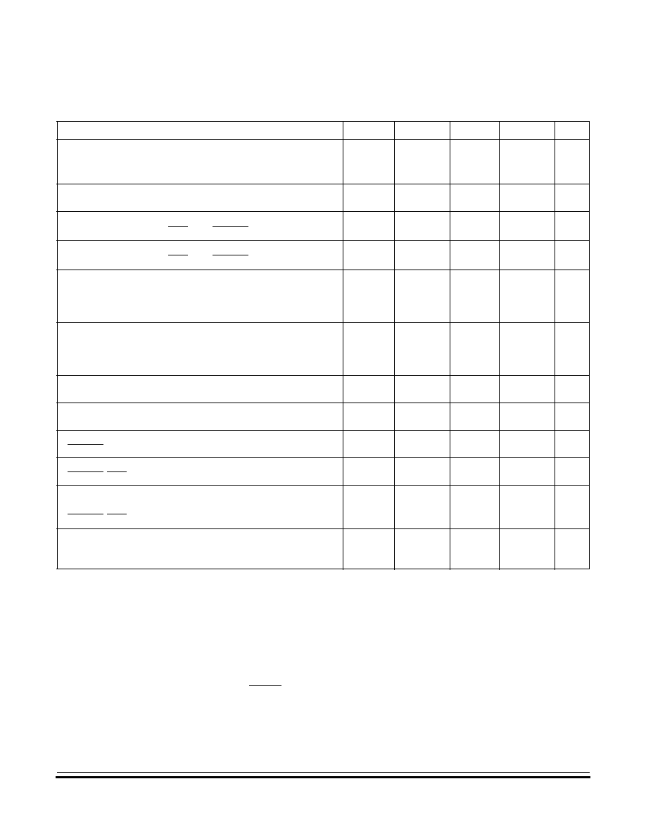
Electrical Specifications
5.0-V DC Electrical Characteristics
MC68HC705KJ1 -- Rev. 2.0
Technical Data
MOTOROLA
Electrical Specifications
117
11.6 5.0-V DC Electrical Characteristics
Characteristic
(1)
1. V
DD
= 5.0 Vdc
±
10%, V
SS
= 0 Vdc, T
A
= ≠40
∞
C to +85
∞
C, unless otherwise noted.
Symbol
Min
Typ
(2)
2. Typical values at midpoint of voltage range, 25
∞
C only
Max
Unit
Output High Voltage
(I
Load
=
≠
2.5 mA) PA4≠PA7
(I
Load
= ≠5.5 mA) PB2≠PB3, PA0≠PA3
V
OH
V
DD
≠0.8
V
DD
≠0.8
--
--
--
--
V
Output Low Voltage
(8)
(I
Load
= 10.0 mA) PA0≠PA7, PB2≠PB3
V
OL
--
--
0.8
V
Input High Voltage
PA0≠PA7, PB2≠PB3, IRQ/V
PP
, RESET, OSC1
V
IH
0.7
◊
V
DD
--
V
DD
V
Input Low Voltage
PA0≠PA7, PB2≠PB3, IRQ/V
PP
, RESET, OSC1
V
IL
V
SS
--
0.2
◊
V
DD
V
Supply Current (f
OP
= 2.1 MHz; f
OSC
= 4.2 MHz)
Run Mode
(3)
Wait Mode
(4)
Stop Mode
(5)
3. Run mode I
DD
is measured using external square wave clock source; all inputs 0.2 V from rail; no dc loads; less than 50 pF
on all outputs; C
L
= 20 pF on OSC2.
4. Wait mode I
DD
: only timer system active. Wait mode is affected linearly by OSC2 capacitance. Wait mode is measured
with all ports configured as inputs; V
IL
= 0.2 V; V
IH
= V
DD
≠ 0.2 V. Wait mode I
DD
is measured using external square wave
clock source; all inputs 0.2 V from rail; no dc loads; less than 50 pF on all outputs; C
L
= 20 pF on OSC2.
5. Stop mode I
DD
is measured with OSC1 = V
SS
. Stop mode I
DD
is measured with all ports configured as inputs; V
IL
= 0.2 V;
V
IH
= V
DD
≠ 0.2 V.
I
DD
--
--
--
4.0
1.0
0.1
6.0
2.8
5.0
mA
mA
µ
A
Supply Current (f
OP
= 4.0 MHz; f
OSC
= 8.0 MHz)
Run Mode
(3)
Wait Mode
(4)
Stop Mode
(5)
I
DD
--
--
--
5.2
1.1
0.1
7.0
3.3
5.0
mA
mA
µ
A
I/O Ports Hi-Z Leakage Current
PA0≠PA7, PB2≠PB3 (Without Individual Pulldown Activated)
I
IL
--
0.2
±
1
µ
A
Input Pulldown Current
PA0≠PA7, PB2≠PB3 (With Individual Pulldown Activated)
I
IL
35
80
200
µ
A
Input Pullup Current
RESET
I
IL
≠15
≠35
≠85
µ
A
Input Current
(6)
RESET, IRQ/V
PP
, OSC1
6. Only input high current rated to +1
µ
A on RESET.
I
In
--
0.2
±
1
µ
A
Capacitance
Ports (As Inputs or Outputs)
RESET, IRQ, OSC1, OSC2
C
Out
C
In
--
--
--
--
12
8
pF
Crystal/Ceramic Resonator Oscillator Mode
Internal Resistor
OSC1 to OSC2
(7)
7. The R
OSC
value selected for RC oscillator versions of this device is unspecified.
8. Maximum current drain for all I/O pins combined should not exceed 100 mA.
R
OSC
1.0
2.0
3.0
M
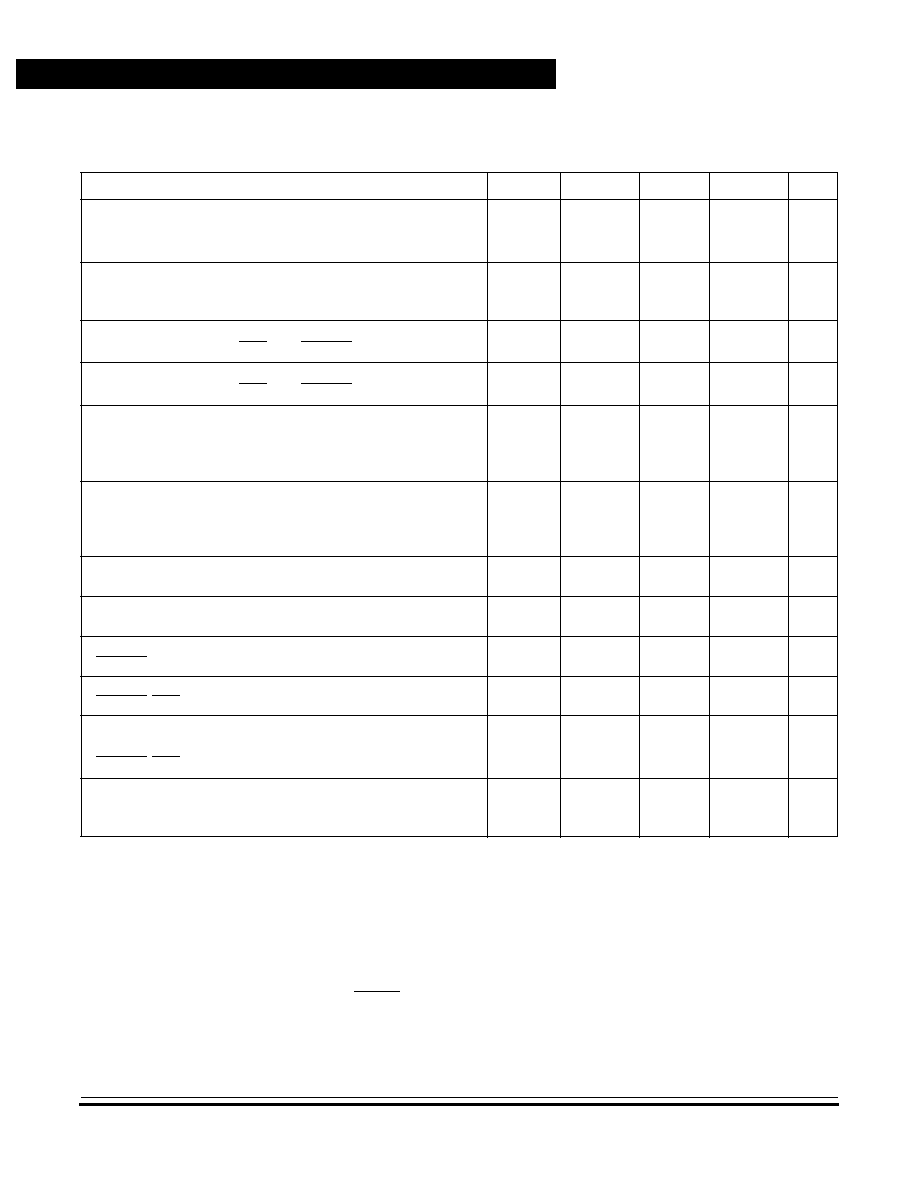
Technical Data
MC68HC705KJ1 -- Rev. 2.0
118
Electrical Specifications
MOTOROLA
Electrical Specifications
11.7 3.3-V DC Electrical Characteristics
Characteristic
(1)
1. V
DD
= 3.3 Vdc
±
10%, V
SS
= 0 Vdc, T
A
= ≠40
∞
C to +85
∞
C, unless otherwise noted.
Symbol
Min
Typ
(2)
2. Typical values at midpoint of voltage range, 25
∞
C only
Max
Unit
Output High Voltage
(I
Load
=
≠
0.8 mA) PA4≠PA7
(I
Load
=
≠
1.5 mA) PA0≠PA3, PB2≠PB3
V
OH
V
DD
≠0.3
V
DD
≠0.3
--
--
--
--
V
Output Low Voltage
(I
Load
= 5.0 mA) PA4≠PA7
(I
Load
= 3.5 mA) PA0≠PA3, PB2≠PB3
V
OL
--
--
--
--
0.5
0.5
V
Input High Voltage
PA0≠PA7, PB2≠PB3, IRQ/V
PP
, RESET, OSC1
V
IH
0.7
◊
V
DD
--
V
DD
V
Input Low Voltage
PA0≠PA7, PB2≠PB3, IRQ/V
PP
, RESET, OSC1
V
IL
V
SS
--
0.2
◊
V
DD
V
Supply Current (f
OP
= 1.0 MHz; f
OSC
= 2.0 MHz)
Run Mode
(3)
Wait Mode
(4)
Stop Mode
(5)
3. Run mode I
DD
is measured using external square wave clock source; all inputs 0.2 V from rail; no dc loads; less than 50 pF
on all outputs; C
L
= 20 pF on OSC2.
4. Wait mode I
DD
: only timer system active. Wait mode is affected linearly by OSC2 capacitance. Wait mode is measured
with all ports configured as inputs; V
IL
= 0.2 V; V
IH
= V
DD
≠ 0.2 V. Wait mode I
DD
is measured using external square wave
clock source; all inputs 0.2 V from rail; no dc loads; less than 50 pF on all outputs; C
L
= 20 pF on OSC2.
5. Stop mode I
DD
is measured with OSC1 = V
SS
. Stop mode I
DD
is measured with all ports configured as inputs; V
IL
= 0.2 V;
V
IH
= V
DD
≠ 0.2 V.
I
DD
--
--
--
1.2
0.3
0.1
2.5
0.8
5.0
mA
mA
µ
A
Supply Current (f
OP
= 2.1 MHz; f
OSC
= 4.2 MHz)
Run Mode
(3)
Wait Mode
(4)
Stop Mode
(5)
I
DD
--
--
--
1.4
0.3
0.1
3.0
1.0
5.0
mA
mA
µ
A
I/O Ports Hi-Z Leakage Current
PA0≠PA7, PB2≠PB3 (Without Individual Pulldown Activated)
I
IL
--
0.1
±
1
µ
A
Input Pulldown Current
PA0≠PA7, PB2≠PB3 (With Individual Pulldown Activated)
I
IL
12
30
100
µ
A
Input Pullup Current
RESET
I
IL
≠10
≠25
≠45
µ
A
Input Current
(6)
RESET, IRQ/V
PP
, OSC1
6. Only input high current rated to +1
µ
A on RESET.
I
In
--
0.1
±
1
µ
A
Capacitance
Ports (As Inputs or Outputs)
RESET, IRQ/V
PP
, OSC1, OSC2
C
Out
C
In
--
--
--
--
12
8
pF
Crystal/Ceramic Resonator Oscillator Mode Internal
Resistor
OSC1 to OSC2
(7)
7. The R
OSC
value selected for RC oscillator versions of this device is unspecified.
R
OSC
1.0
2.0
3.0
M
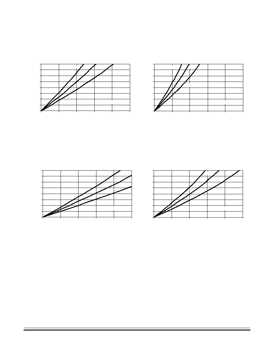
Electrical Specifications
Driver Characteristics
MC68HC705KJ1 -- Rev. 2.0
Technical Data
MOTOROLA
Electrical Specifications
119
11.8 Driver Characteristics
Figure 11-1. PA4≠PA7 Typical High-Side Driver Characteristics
Figure 11-2. PA0≠PA3 and PB2≠PB3 Typical High-Side Driver Characteristics
Notes:
1. At V
DD
= 5.0 V, devices are specified and tested for (V
DD
≠ V
OH
)
800 mV @ I
OH
= ≠2.5 mA.
2. At V
DD
= 3.3 V, devices are specified and tested for (V
DD
≠ V
OH
)
300 mV @ I
OH
= ≠0.8 mA.
0
100
200
300
400
500
600
700
800
0
≠2
≠4
≠6
≠8
≠10
I
OH
(mA)
V
DD
≠ V
OH
(mV)
≠40
∞
C
85
∞
C
25
∞
C
V
DD
= 3.3 V
0
100
200
300
400
500
600
700
800
0
≠2
≠4
≠6
≠8
≠10
I
OH
(mA)
V
DD
≠ V
OH
(mV)
≠40
∞
C
85
∞
C
25
∞
C
V
DD
= 5.0 V
Notes:
1. At V
DD
= 5.0 V, devices are specified and tested for (V
DD
≠ V
OH
)
800 mV @ I
OH
= ≠5.5 mA.
2. At V
DD
= 3.3 V, devices are specified and tested for (V
DD
≠ V
OH
)
300 mV @ I
OH
= ≠1.5 mA.
0
100
200
300
400
500
600
700
800
0
≠2
≠4
≠6
≠8
≠10
I
OH
(mA)
V
DD
≠ V
OH
(mV)
≠40
∞
C
25
∞
C
V
DD
= 3.3 V
85
∞
C
0
100
200
300
400
500
600
700
800
0
≠2
≠4
≠6
≠8
≠10
I
OH
(mA)
V
DD
≠ V
OH
(mV)
≠40
∞
C
85
∞
C
25
∞
C
V
DD
= 5.0 V
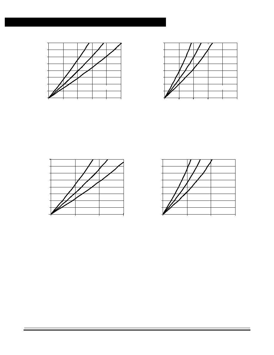
Technical Data
MC68HC705KJ1 -- Rev. 2.0
120
Electrical Specifications
MOTOROLA
Electrical Specifications
Figure 11-3. PA4≠PA7 Typical Low-Side Driver Characteristics
Figure 11-4. PA0≠PA3 and PB2≠PB3 Typical Low-Side Driver Characteristics
Notes:
1. At V
DD
= 5.0 V, devices are specified and tested for V
OL
800 mV @ I
OL
= 10.0 mA.
2. At V
DD
= 3.3 V, devices are specified and tested for V
OL
500 mV @ I
OL
= 5.0 mA.
0
100
200
300
400
500
600
700
800
0
10
20
30
40
50
≠40
∞
C
25
∞
C
85
∞
C
V
DD
= 3.3 V
0
100
200
300
400
500
600
700
800
0
10
20
30
40
50
≠40
∞
C
25
∞
C
I
OL
(mA)
V
OL
(mV)
85
∞
C
V
DD
= 5.0 V
V
OL
(mV)
I
OL
(mA)
Notes:
1. At V
DD
= 5.0 V, devices are specified and tested for V
OL
800 mV @ I
OL
= 10.0 mA.
2. At V
DD
= 3.3 V, devices are specified and tested for V
OL
500 mV @ I
OL
= 3.5 mA.
0
100
200
300
400
500
600
700
800
0
10
20
30
≠40
∞
C
25
∞
C
85
∞
C
V
DD
= 3.3 V
0
100
200
300
400
500
600
700
800
0
10
20
30
≠40
∞
C
25
∞
C
85
∞
C
V
DD
= 5.0 V
V
OL
(mV)
V
OL
(mV)
I
OL
(mA)
I
OL
(mA)
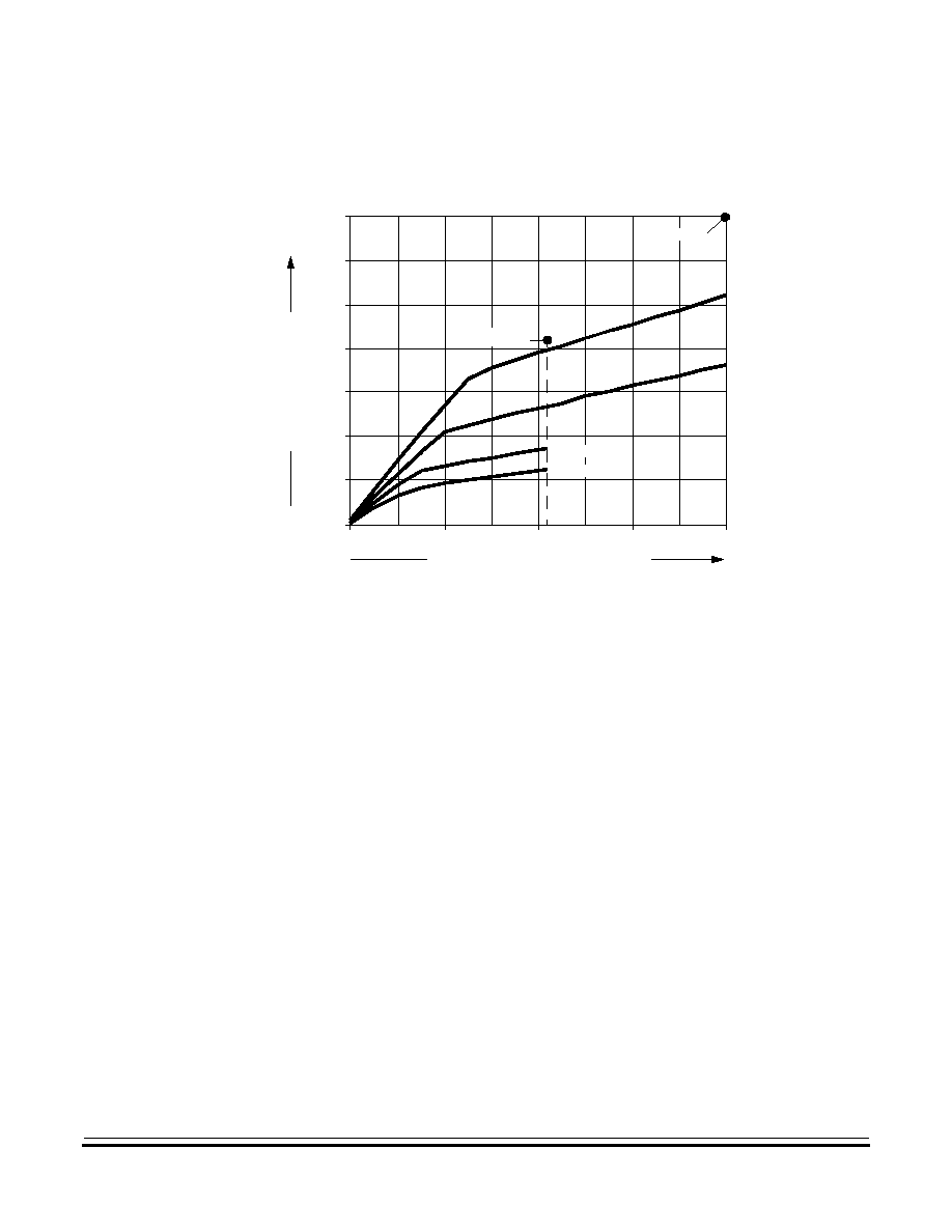
Electrical Specifications
Typical Supply Currents
MC68HC705KJ1 -- Rev. 2.0
Technical Data
MOTOROLA
Electrical Specifications
121
11.9 Typical Supply Currents
Figure 11-5. Typical Operating I
DD
(25
∞
C)
6.0 mA
5.0 mA
4.0 mA
3.0 mA
2.0 mA
1.0 mA
0
0
1.0 MHz
2.0 MHz
3.0 MHz
4.0 MHz
3.0 V
4.5 V
3.6 V
5.5 V
SUPPLY CURRENT (I
DD
)
INTERNAL OPERATING FREQUENCY (f
OP
)
Notes:
1. At V
DD
= 5.0 V, devices are specified and tested for
I
DD
7.0 mA @ f
OP
= 4.0 MHz.
2. At V
DD
= 3.3 V, devices are specified and tested for
I
DD
4.25 mA @ f
OP
= 2.1 MHz.
SEE NOTE 1
SEE NOTE 2
7.0 mA
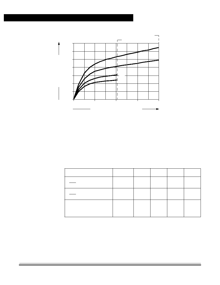
Technical Data
MC68HC705KJ1 -- Rev. 2.0
122
Electrical Specifications
MOTOROLA
Electrical Specifications
Figure 11-6. Typical Wait Mode I
DD
(25
∞
C)
11.10 EPROM Programming Characteristics
Characteristic
(1)
1.
V
DD
= 5.0 Vdc
±
10%, V
SS
= 0 Vdc, T
A
=
≠
40
∞
C to +85
∞
C, unless otherwise noted.
Symbol
Min
Typ
Max
Unit
Programming Voltage
IRQ/V
PP
V
PP
16.0
16.5
17.0
V
Programming Current
IRQ/V
PP
I
PP
--
3.0
10.0
mA
Programming Time
Per Array Byte
MOR
t
EPGM
t
MPGM
4
4
--
--
--
--
ms
700
µ
A
600
µ
A
500
µ
A
400
µ
A
300
µ
A
200
µ
A
100
µ
A
0
0
1.0 MHz
2.0 MHz
3.0 MHz
4.0 MHz
3.0 V
4.5 V
3.6 V
5.5 V
SUPPLY CURRENT (I
DD
)
INTERNAL OPERATING FREQUENCY (f
OP
)
Notes:
1. At V
DD
= 5.0 V, devices are specified and tested for
I
DD
3.25 mA @ f
OP
= 4.0 MHz.
2. At V
DD
= 3.3 V, devices are specified and tested for
I
DD
1.75 mA @ f
OP
= 2.1 MHz.
SEE NOTE 1
SEE NOTE 2
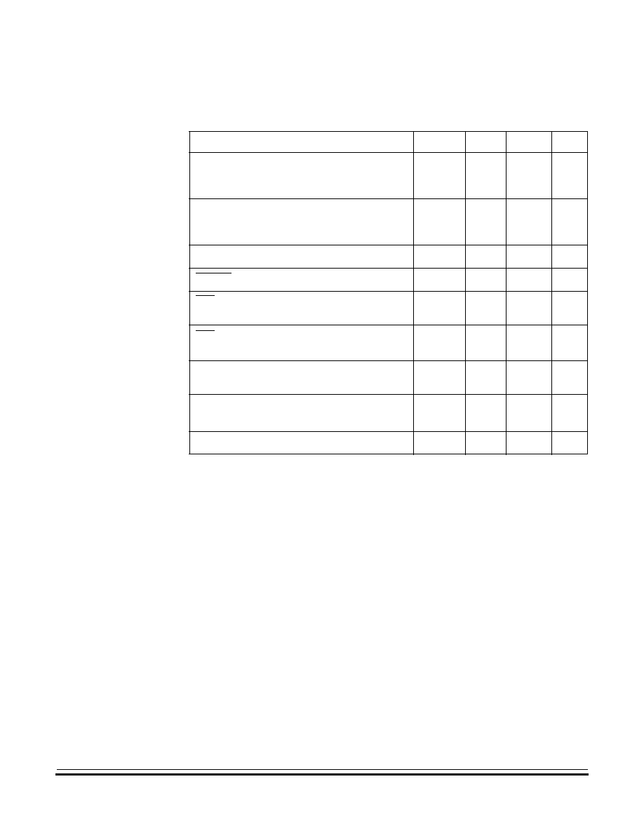
Electrical Specifications
Control Timing
MC68HC705KJ1 -- Rev. 2.0
Technical Data
MOTOROLA
Electrical Specifications
123
11.11 Control Timing
Table 11-2. Control Timing (V
DD
= 5.0 Vdc)
(1)
1. V
DD
= 5.0 Vdc
±
10%, V
SS
= 0 Vdc,
T
A
=
≠
40
∞
C to +85
∞
C,
unless otherwise noted.
Characteristic
Symbol
Min
Max
Unit
Oscillator Frequency
Crystal Oscillator Option
External Clock Source
f
OSC
--
dc
8.0
8.0
MHz
Internal Operating Frequency (f
OSC
˜
2)
Crystal Oscillator
External Clock
f
OP
--
dc
4.0
4.0
MHz
Cycle Time (1
˜
f
OP
)
t
cyc
250
--
ns
RESET Pulse Width Low
t
RL
1.5
--
t
cyc
IRQ Interrupt Pulse Width Low
(Edge-Triggered)
t
ILIH
1.5
--
t
cyc
IRQ Interrupt Pulse Width Low
(Edge- and Level-Triggered)
t
ILIL
1.5
Note
(2)
2. The maximum width t
ILIL
or t
ILIH
should not be more than the number of cycles it takes to
execute the interrupt service routine plus 19 t
cyc
or the interrupt service routine will be
re-entered.
t
cyc
PA0≠PA3 Interrupt Pulse Width High
(Edge-Triggered)
t
IHIL
1.5
--
t
cyc
PA0≠PA3 Interrupt Pulse Width
(Edge- and Level-Triggered)
t
IHIH
1.5
Note
(2)
t
cyc
OSC1 Pulse Width
t
OH
, t
OL
100
--
ns
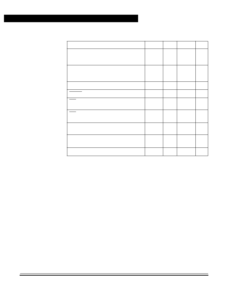
Technical Data
MC68HC705KJ1 -- Rev. 2.0
124
Electrical Specifications
MOTOROLA
Electrical Specifications
Table 11-3. Control Timing (V
DD
= 3.3 Vdc)
(1)
1. V
DD
= 3.3 Vdc
±
10%, V
SS
= 0 Vdc,
T
A
=
≠
40
∞
C to +85
∞
C,
unless otherwise noted.
Characteristic
Symbol
Min
Max
Unit
Oscillator Frequency
Crystal Oscillator Option
External Clock Source
f
OSC
--
dc
4.2
4.2
MHz
Internal Operating Frequency (f
OSC
˜
2)
Crystal Oscillator
External Clock
f
OP
--
dc
2.1
2.1
MHz
Cycle Time (1
˜
f
OP
)
t
cyc
476
--
ns
RESET Pulse Width Low
t
RL
1.5
--
t
cyc
IRQ Interrupt Pulse Width Low
(Edge-Triggered)
t
ILIH
1.5
--
t
cyc
IRQ Interrupt Pulse Width Low
(Edge- and Level-Triggered)
t
ILIL
1.5
Note
(2)
2. The maximum width t
ILIL
or t
ILIH
should not be more than the number of cycles it takes to
execute the interrupt service routine plus 19 t
cyc
or the interrupt service routine will be
re-entered.
t
cyc
PA0≠PA3 Interrupt Pulse Width High
(Edge-Triggered)
t
IHIL
1.5
--
t
cyc
PA0≠PA3 Interrupt Pulse Width
(Edge- and Level-Triggered)
t
IHIH
1.5
Note
(2)
t
cyc
OSC1 Pulse Width
t
OH
, t
OL
200
--
ns
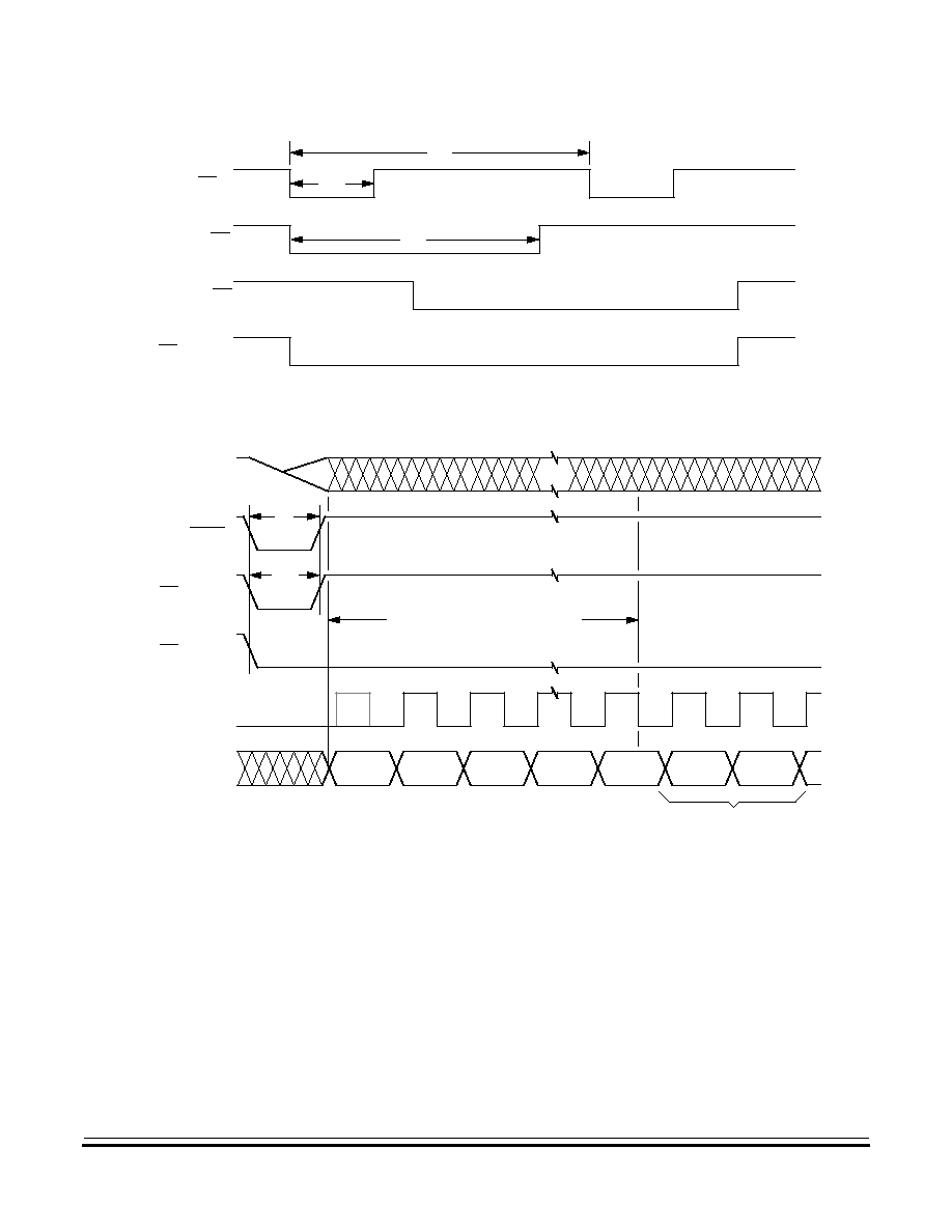
Electrical Specifications
Control Timing
MC68HC705KJ1 -- Rev. 2.0
Technical Data
MOTOROLA
Electrical Specifications
125
Figure 11-7. External Interrupt Timing
Figure 11-8. Stop Mode Recovery Timing
IRQ (INTERNAL)
t
ILIH
t
ILIL
t
ILIH
IRQ PIN
IRQ
1
IRQ
n
.
.
.
t
ILIH
OSCILLATOR STABILIZATION DELAY
(5)
OSC (NOTE 1)
t
RL
RESET
IRQ (NOTE 2)
IRQ (NOTE 3)
INTERNAL
CLOCK
INTERNAL
ADDRESS BUS
Notes:
1. Internal clocking from OSC1 pin
2. Edge-triggered external interrupt mask option
3. Edge- and level-triggered external interrupt mask option
4. Reset vector shown as example
RESET OR INTERRUPT
VECTOR FETCH
07FE
07FE
07FE
07FE
07FE
07FF
(NOTE 4)
5. 4064 t
cyc
or 128 t
cyc
, depending on the state of SOSCD bit in MOR
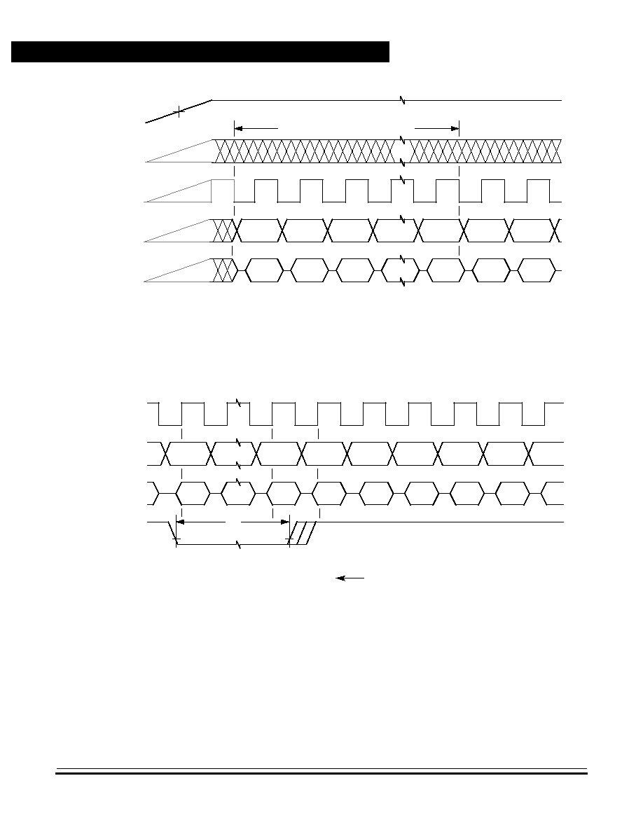
Technical Data
MC68HC705KJ1 -- Rev. 2.0
126
Electrical Specifications
MOTOROLA
Electrical Specifications
Figure 11-9. Power-On Reset Timing
Figure 11-10. External Reset Timing
07FE
OSCILLATOR STABILIZATION DELAY
(3)
V
DD
OSC1 PIN
INTERNAL
CLOCK
INTERNAL
ADDRESS BUS
NOTES:
INTERNAL
DATA BUS
07FE
07FE
07FE
07FE
07FE
07FF
(NOTE 1)
1. Power-on reset threshold is typically between 1 V and 2 V.
2. Internal clock, internal address bus, and internal data bus are not available externally.
NEW
PCH
NEW
PCL
3. 4064 t
cyc
or 128 t
cyc
depending on the state of SOSCD bit in MOR
INTERNAL
CLOCK
INTERNAL
ADDRESS BUS
NOTES:
INTERNAL
DATA BUS
07FE
07FE
07FE
07FE
07FF
NEW PC
1. Internal clock, internal address bus, and internal data bus are not available externally.
2. The next rising edge of the internal clock after the rising edge of RESET initiates the reset sequence.
NEW
PCH
t
RL
NEW PC
NEW
PCL
DUMMY
OP
CODE

MC68HC705KJ1 -- Rev. 2.0
Technical Data
MOTOROLA
Mechanical Specifications
127
Technical Data -- MC68HC705KJ1
Section 12. Mechanical Specifications
12.1 Contents
12.2
Introduction . . . . . . . . . . . . . . . . . . . . . . . . . . . . . . . . . . . . . . .127
12.2.1
16-Pin PDIP -- Case #648. . . . . . . . . . . . . . . . . . . . . . . . .128
12.2.2
16-Pin SOIC -- Case #751G . . . . . . . . . . . . . . . . . . . . . . .128
12.2.3
16-Pin Cerdip -- Case #620A . . . . . . . . . . . . . . . . . . . . . .129
12.2 Introduction
The MC68HC705J1A, the RC oscillator, and low-speed option devices
described in
Appendix A. MC68HRC705KJ1
and
Appendix B.
MC68HLC705KJ1
are available in these packages:
∑
648 -- Plastic dual in-line package (PDIP)
∑
751G -- Small outline integrated circuit (SOIC)
∑
620A -- Ceramic DIP (Cerdip) (windowed)
The following figures show the latest packages at the time of this
publication. To make sure that you have the latest package
specifications, contact one of the following:
∑
Local Motorola Sales Office
∑
Motorola Mfax
≠
Phone 602-244-6609
≠
Email rmfax0@email.sps.mot.com
∑
World-Wide Web (wwweb) at http://motorola.com/sps/
Follow Mfax or World-Wide Web on-line instructions to retrieve the
current mechanical specifications.

Technical Data
MC68HC705KJ1 -- Rev. 2.0
128
Mechanical Specifications
MOTOROLA
Mechanical Specifications
12.2.1 16-Pin PDIP -- Case #648
12.2.2 16-Pin SOIC -- Case #751G
NOTES:
1. DIMENSIONING AND TOLERANCING PER ANSI
Y14.5M, 1982.
2. CONTROLLING DIMENSION: INCH.
3. DIMENSION L TO CENTER OF LEADS WHEN
FORMED PARALLEL.
4. DIMENSION B DOES NOT INCLUDE MOLD FLASH.
5. ROUNDED CORNERS OPTIONAL.
≠A≠
B
F
C
S
H
G
D
J
L
M
16 PL
SEATING
1
8
9
16
K
PLANE
≠T≠
M
A
M
0.25 (0.010)
T
DIM
MIN
MAX
MIN
MAX
MILLIMETERS
INCHES
A
0.740
0.770
18.80
19.55
B
0.250
0.270
6.35
6.85
C
0.145
0.175
3.69
4.44
D
0.015
0.021
0.39
0.53
F
0.040
0.70
1.02
1.77
G
0.100 BSC
2.54 BSC
H
0.050 BSC
1.27 BSC
J
0.008
0.015
0.21
0.38
K
0.110
0.130
2.80
3.30
L
0.295
0.305
7.50
7.74
M
0
10
0
10
S
0.020
0.040
0.51
1.01
_
_
_
_
F
J
DIM
MIN
MAX
MIN
MAX
INCHES
MILLIMETERS
A
10.15
10.45
0.400
0.411
B
7.40
7.60
0.292
0.299
C
2.35
2.65
0.093
0.104
D
0.35
0.49
0.014
0.019
F
0.50
0.90
0.020
0.035
G
1.27 BSC
0.050 BSC
J
0.25
0.32
0.010
0.012
K
0.10
0.25
0.004
0.009
M
0
∞
7
∞
0
∞
7
∞
P
10.05
10.55
0.395
0.415
R
0.25
0.75
0.010
0.029
M
B
M
0.010 (0.25)
-A-
-B-
P
8X
G
14X
D
16X
SEATING
PLANE
-T-
S
A
M
0.010 (0.25)
B S
T
16
9
8
1
R
X 45
M
C
K
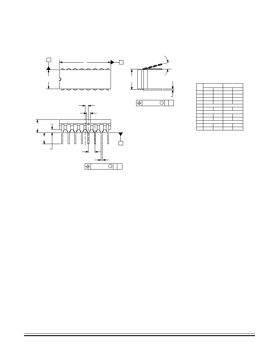
Mechanical Specifications
Introduction
MC68HC705KJ1 -- Rev. 2.0
Technical Data
MOTOROLA
Mechanical Specifications
129
12.2.3 16-Pin Cerdip -- Case #620A
NOTES:
1. DIMENSIONING AND TOLERANCING PER
ASME Y14.5M, 1994.
2. CONTROLLING DIMENSION: INCH.
3. DIMENSION L TO CENTER OF LEAD WHEN
FORMED PARALLEL.
4. DIMENSION F MAY NARROW TO 0.76 (0.030)
WHERE THE LEAD ENTERS THE CERAMIC
BODY.
STYLE 1:
PIN 1.
CATHODE
2.
CATHODE
3.
CATHODE
4.
CATHODE
5.
CATHODE
6.
CATHODE
7.
CATHODE
8.
CATHODE
9.
ANODE
10.
ANODE
F
E
N
K
C
SEATING
PLANE
A
M
0.25 (0.010)
T
M
L
DIM
MIN
MAX
MIN
MAX
MILLIMETERS
INCHES
A
0.750
0.785
19.05
19.93
B
0.240
0.295
6.10
7.49
C
≠≠≠
0.200
≠≠≠
5.08
D
0.015
0.020
0.39
0.50
E
0.050 BSC
1.27 BSC
F
0.055
0.065
1.40
1.65
G
0.100 BSC
2.54 BSC
H
0.008
0.015
0.21
0.38
K
0.125
0.170
3.18
4.31
L
0.300 BSC
7.62 BSC
M
0
15
0
15
N
0.020
0.040
0.51
1.01
_
_
_
_
A
B
A
B
16
1
9
8
G
16X
D
B
M
0.25 (0.010)
T
T
16X
J

Technical Data
MC68HC705KJ1 -- Rev. 2.0
130
Mechanical Specifications
MOTOROLA
Mechanical Specifications
MC68HC705KJ1 -- Rev. 2.0
Technical Data
MOTOROLA
Ordering Information
131
Technical Data -- MC68HC705KJ1
Section 13. Ordering Information
13.1 Contents
13.2
Introduction . . . . . . . . . . . . . . . . . . . . . . . . . . . . . . . . . . . . . . .131
13.3
MCU Order Numbers . . . . . . . . . . . . . . . . . . . . . . . . . . . . . . .131
13.2 Introduction
This section contains ordering information for the available package
types.
13.3 MCU Order Numbers
Table 13-1
lists the MC order numbers.
Table 13-1. Order Numbers
(1)
1. Refer to
Appendix A. MC68HRC705KJ1
and
Appendix B. MC68HLC705KJ1
for order-
ing information on optional low-speed and resistor-capacitor oscillator devices.
Package
Type
Case
Outline
Pin
Count
Operating
Temperature
Order Number
PDIP
648
16
≠40 to +85
∞
C
MC68HC705KJ1C
(2)
2. C = extended temperature range
SOIC
751G
16
≠40 to +85
∞
C
MC68HC705KJ1CDW
(3)
3. DW = small outline integrated circuit (SOIC)
Cerdip
620A
16
≠40 to +85
∞
C
MC68HC705KJ1CS
(4)
4. S = ceramic dual in-line package (Cerdip)

Technical Data
MC68HC705KJ1 -- Rev. 2.0
132
Ordering Information
MOTOROLA
Ordering Information

MC68HC705KJ1 -- Rev. 2.0
Technical Data
MOTOROLA
MC68HRC705KJ1
133
Technical Data -- MC68HC705KJ1
Appendix A. MC68HRC705KJ1
A.1 Contents
A.2
Introduction . . . . . . . . . . . . . . . . . . . . . . . . . . . . . . . . . . . . . . .133
A.3
RC Oscillator Connections . . . . . . . . . . . . . . . . . . . . . . . . . . .134
A.4
Typical Internal Operating Frequency for
RC Oscillator Option . . . . . . . . . . . . . . . . . . . . . . . . . . . . .135
A.5
RC Oscillator Connections (No External Resistor) . . . . . . . . .136
A.6
Typical Internal Operating Frequency Versus Temperature
(No External Resistor) . . . . . . . . . . . . . . . . . . . . . . . . . . . .137
A.7
Package Types and Order Numbers . . . . . . . . . . . . . . . . . . .138
A.2 Introduction
This appendix introduces the MC68HRC705KJ1, a resistor-capacitor
(RC) oscillator mask option version of the MC68HC705KJ1. All of the
information in MC68HC705KJ1 Technical Data applies to the
MC68HRC705KJ1 with the exceptions given in this appendix.
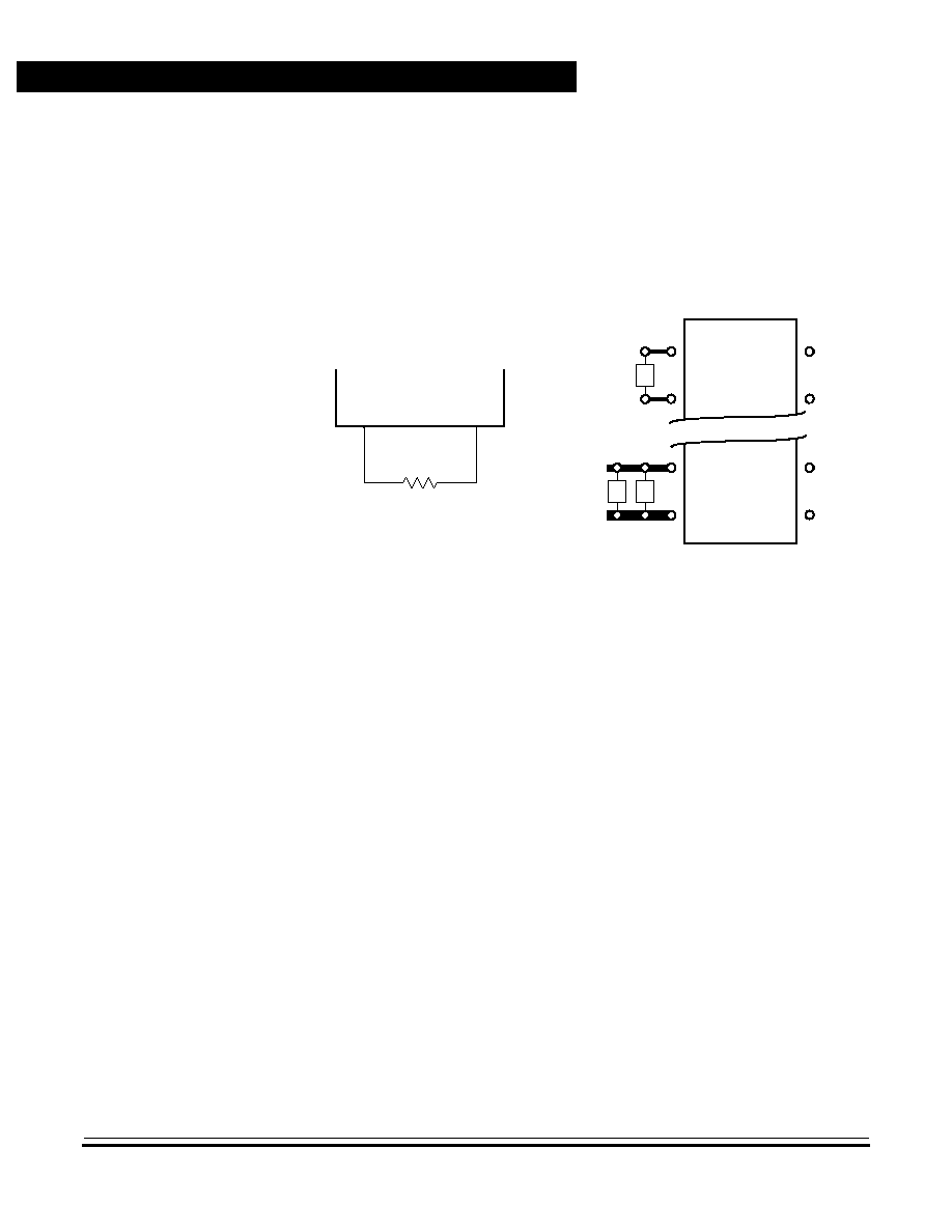
Technical Data
MC68HC705KJ1 -- Rev. 2.0
134
MC68HRC705KJ1
MOTOROLA
MC68HRC705KJ1
A.3 RC Oscillator Connections
For greater cost reduction, the RC oscillator mask option allows the
configuration shown in
Figure A-1
to drive the on-chip oscillator. Mount
the RC components as close as possible to the pins for startup
stabilization and to minimize output distortion.
Figure A-1. RC Oscillator Connections
NOTE:
The optional internal resistor is not recommended for configurations that
use the RC oscillator connections as shown in
Figure A-1
. For such
configurations, the oscillator internal resistor (OSCRES) bit of the mask
option register should be programmed to a logic 0.
MCU
V
DD
V
SS
C1
C2
OSC1
OSC2
R
OSC1
OSC2
R
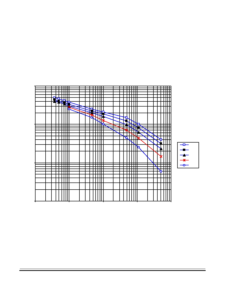
MC68HRC705KJ1
Typical Internal Operating Frequency for RC Oscillator Option
MC68HC705KJ1 -- Rev. 2.0
Technical Data
MOTOROLA
MC68HRC705KJ1
135
A.4 Typical Internal Operating Frequency for RC Oscillator Option
Figure A-2
shows typical internal operating frequencies at 25
∞
C for the
RC oscillator option.
NOTE:
Tolerance for resistance is
±
50%. When selecting resistor size, consider
the tolerance to ensure that the resulting oscillator frequency does not
exceed the maximum operating frequency.
Figure A-2. Typical Internal Operating Frequency
for Various V
DD
at 25
∞
C -- RC Oscillator Option Only
0.01
0.1
1
10
1
10
100
1000
10000
RESISTANCE (k
)
5.5 V
5.0 V
4.5 V
3.6 V
3.0 V
FREQUENCY
(MHz)
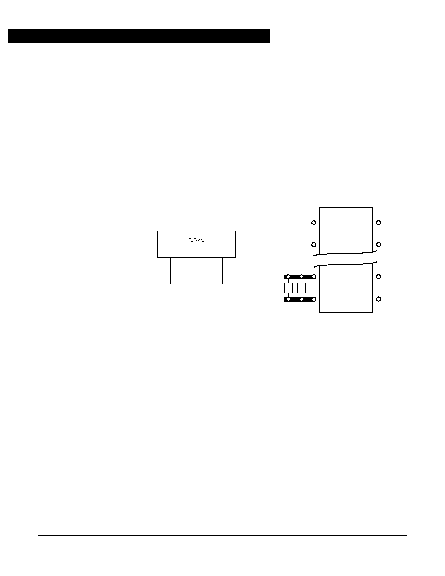
Technical Data
MC68HC705KJ1 -- Rev. 2.0
136
MC68HRC705KJ1
MOTOROLA
MC68HRC705KJ1
A.5 RC Oscillator Connections (No External Resistor)
For maximum cost reduction, the RC oscillator mask connections shown
in
Figure A-3
allow the on-chip oscillator to be driven with no external
components. This can be accomplished by programming the oscillator
internal resistor (OSCRES) bit in the mask option register to a logic 1.
When programming the OSCRES bit for the MC68HSR705KJ1, an
internal resistor is selected which yields typical internal oscillator
frequencies as shown in
Figure A-4
. The internal resistance for this
device is different than the resistance of the selectable internal resistor
on the MC68HC705KJ1 and the MC68HSC705KJ1 devices.
Figure A-3. RC Oscillator Connections (No External Resistor)
MCU
V
DD
V
SS
C1
C2
OSC1
OSC2
OSC1
OSC2
R
(EXTERNAL CONNECTIONS LEFT OPEN)
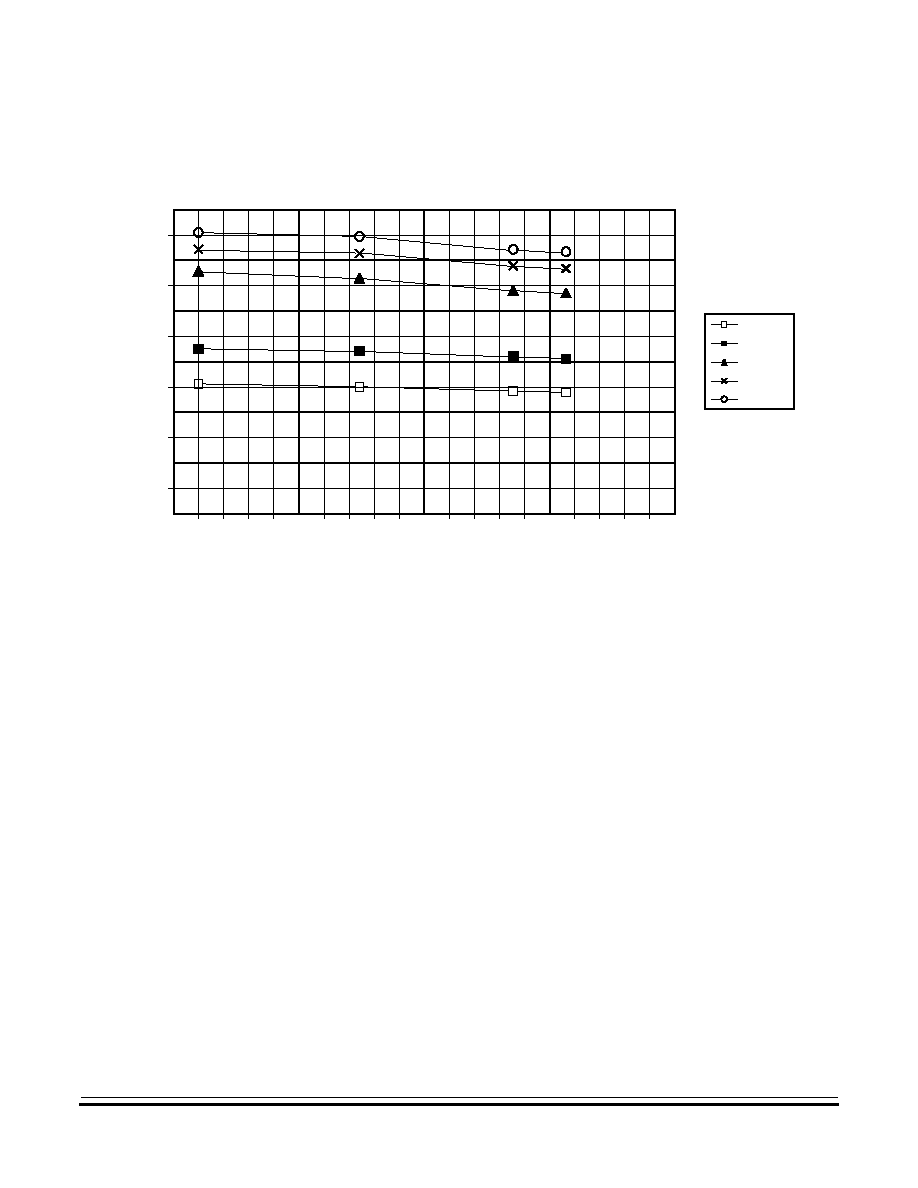
MC68HRC705KJ1
Typical Internal Operating Frequency Versus Temperature (No External Resistor)
MC68HC705KJ1 -- Rev. 2.0
Technical Data
MOTOROLA
MC68HRC705KJ1
137
A.6 Typical Internal Operating Frequency Versus Temperature
(No External Resistor)
Figure A-4. Typical Internal Operating Frequency
Versus Temperature (OSCRES Bit = 1)
NOTE:
Due to process variations, operating voltages, and temperature
requirements, the internal resistance and tolerance are unspecified.
Typically for a given voltage and temperature, the frequency should not
vary more than
±
500 kHz. However, this data is not guaranteed. It is the
user's responsibility to ensure that the resulting internal operating
frequency meets user's requirements.
3.0 V
3.6 V
4.5 V
5.0 V
5.5 V
Frequency (MHz)
Temperature (
∞
C)
3.00
2.50
2.00
1.50
1.00
0.50
0.00
≠50
0
50
100
150

Technical Data
MC68HC705KJ1 -- Rev. 2.0
138
MC68HRC705KJ1
MOTOROLA
MC68HRC705KJ1
A.7 Package Types and Order Numbers
Table A-1. MC68HRC705KJ1 (RC Oscillator Option) Order
Numbers
(1)
1. Refer to
Section 13. Ordering Information
for standard part ordering information.
Package
Type
Case
Outline
Pin
Count
Operating
Temperature
Order Number
PDIP
648
16
≠40 to +85
∞
C
MC68HRC705KJ1C
(2)
P
(3)
2. C = extended temperature range
3. P = plastic dual in-line package (PDIP)
SOIC
751G
16
≠40 to +85
∞
C
MC68HRC705KJ1CDW
(4)
4. DW = small outline integrated circuit (SOIC)
Cerdip
620A
16
≠40 to +85
∞
C
MC68HRC705KJ1CS
(5)
5. S = ceramic dual in-line package (Cerdip)
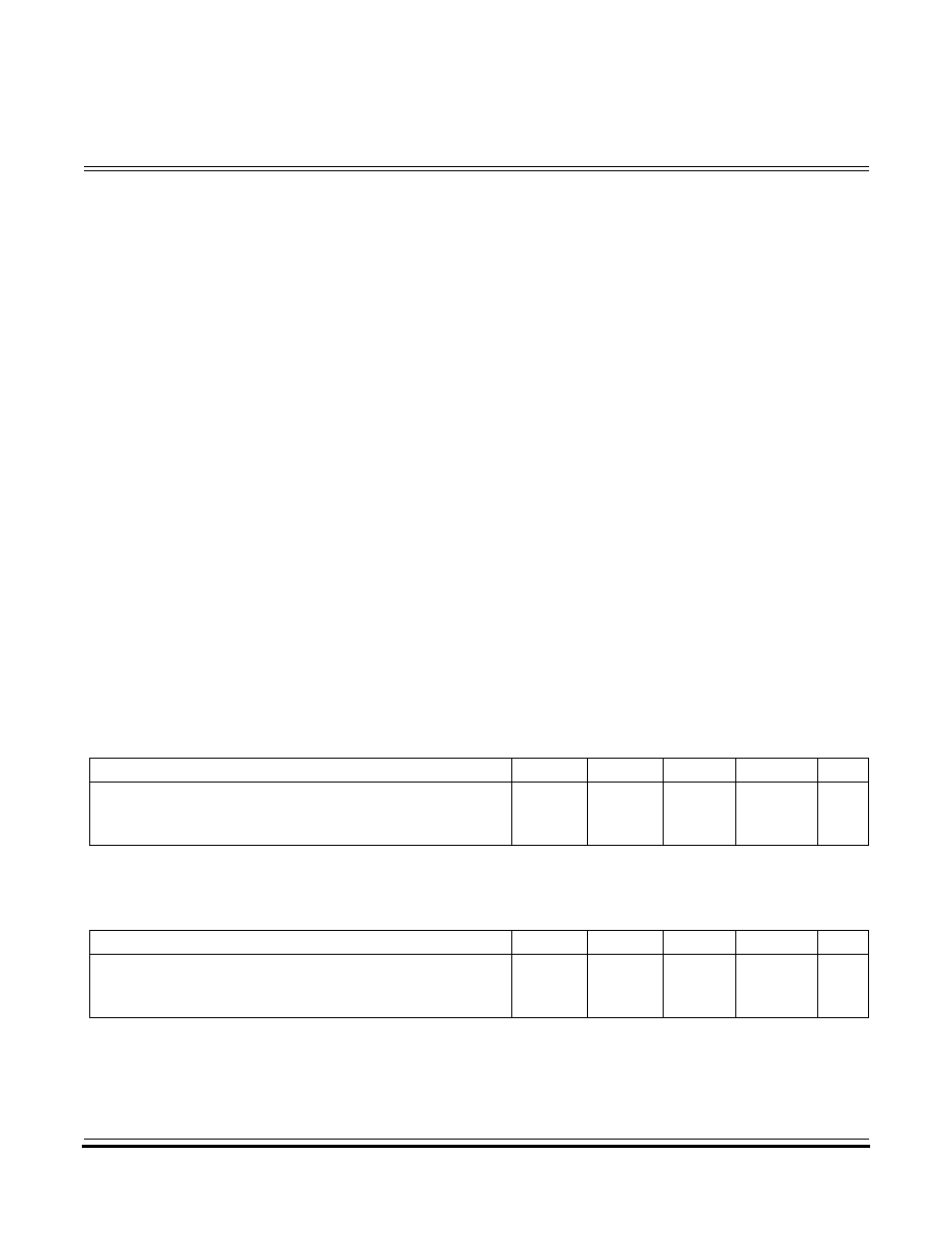
MC68HC705KJ1 -- Rev. 2.0
Technical Data
MOTOROLA
MC68HLC705KJ1
139
Technical Data -- MC68HC705KJ1
Appendix B. MC68HLC705KJ1
B.1 Contents
B.2
Introduction . . . . . . . . . . . . . . . . . . . . . . . . . . . . . . . . . . . . . . .139
B.3
DC Electrical Characteristics . . . . . . . . . . . . . . . . . . . . . . . . .139
B.4
Package Types and Order Numbers . . . . . . . . . . . . . . . . . . .140
B.2 Introduction
This appendix introduces the MC68HLC705KJ1, a low-frequency
version of the MC68HC705KJ1 optimized for 32-kHz oscillators. All of
the information in MC68HC705KJ1 Technical Data applies to the
MC68HLC705KJ1 with the exceptions given in this appendix.
B.3 DC Electrical Characteristics
Table B-1. DC Electrical Characteristics (V
DD
= 5 V)
Characteristic
Symbol
Min
Typ
Max
Unit
Supply Current (f
OP
= 16.0 kHz, f
OSC
= 32.0 kHz)
Run
Wait
I
DD
--
--
45
20
60
30
µ
A
Table B-2. DC Electrical Characteristics (V
DD
= 3.3 V)
Characteristic
Symbol
Min
Typ
Max
Unit
Supply Current (f
OP
= 16.0 kHz, f
OSC
= 32.0 kHz)
Run
Wait
I
DD
--
--
25
10
35
15
µ
A
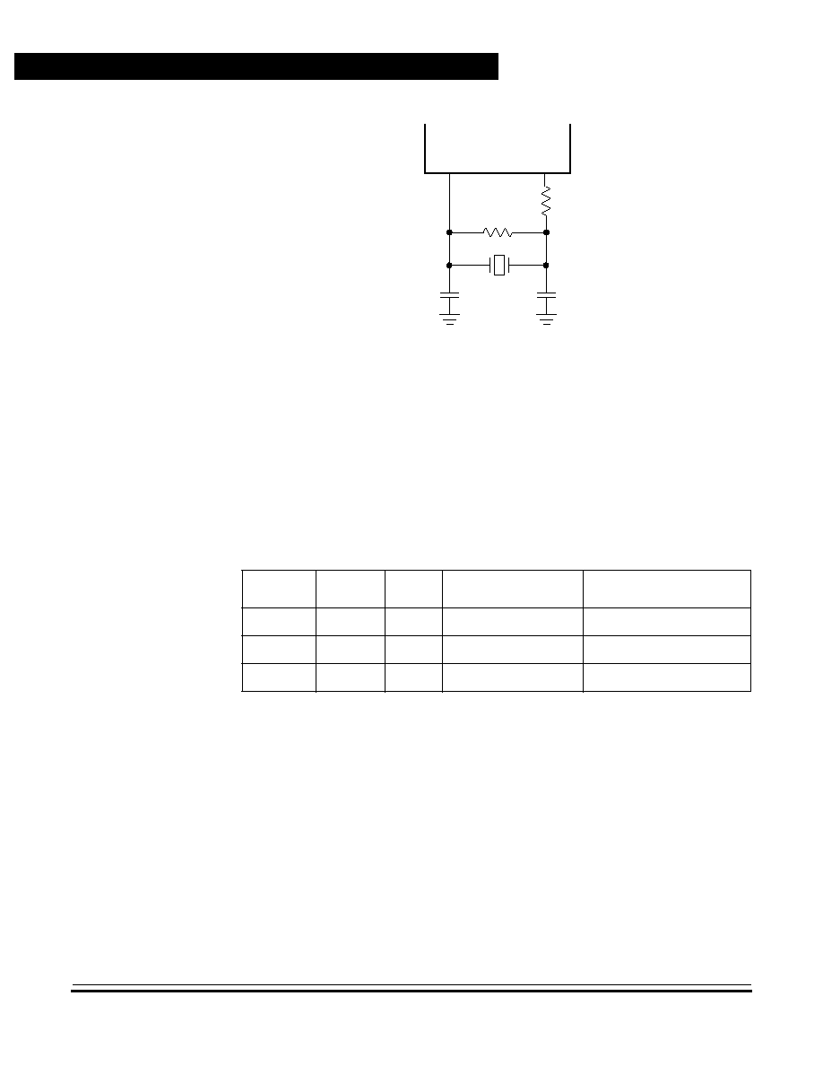
Technical Data
MC68HC705KJ1 -- Rev. 2.0
140
MC68HLC705KJ1
MOTOROLA
MC68HLC705KJ1
Figure B-1. Crystal Connections
NOTE:
Supply current is impacted by crystal type and external components.
Since each crystal has its own characteristics, the user should consult
the crystal manufacturer for appropriate values for external components.
B.4 Package Types and Order Numbers
MCU
R
P
R
S
OSC1
32 kHz
C
L
C
L
Table B-3. MC68HLC705KJ1 (High Speed) Order Numbers
(1)
1. Refer to
Section 13. Ordering Information
for standard part ordering information.
Package
Type
Case
Outline
Pin
Count
Operating
Temperature
Order Number
PDIP
648
16
≠40 to +85
∞
C
MC68HLC705KJ1C
(2)
P
2. C = extended temperature range
SOIC
751G
16
≠40 to +85
∞
C
MC68HLC705KJ1CDW
(3)
3. DW = small outline integrated circuit (SOIC)
Cerdip
620A
16
≠40 to +85
∞
C
MC68HLC705KJ1CS
(4)
4. S = ceramic dual in-line package (Cerdip)
MC68HC705KJ1 Rev. 2.0
Technical Data Book
Please help us to continue improving the quality and usefulness of our data books by
completing this form and sending your comments to us. You can return the form by mail
or FAX it to 512-891-3236.
Thank you for your help and continued support!
1. How do you rate the quality of this data book?
2. Are you able to find the information you need easily?
3. What are your recommendations for making this data book more useful?
4. What additional information would you like to see included in future data books?
High
Low
High
Low
Organization
Tables
Readability
Table of contents
Accuracy
Page size/binding
Figures
Overall impression
Yes
No

First: cut along this line to remove
Motorola
6501 William Cannon Drive West
Mail Stop OE17
Austin, Texas 78735-8598
Attention: MMD Publications Department
Second: fold back along this line
Please supply the following information (optional).
Name: ____________________________________________________________
Company Name: ____________________________________________________
Title: ______________________________________________________________
Address:___________________________________________________________
City: __________________________________________State:______Zip:_______
Phone Number: _____________________________________________________
USA
PLEASE
PASTE
POSTAGE
HERE


Motorola reserves the right to make changes without further notice to any products herein. Motorola makes no warranty, representation or guarantee regarding
the suitability of its products for any particular purpose, nor does Motorola assume any liability arising out of the application or use of any product or circuit, and
specifically disclaims any and all liability, including without limitation consequential or incidental damages. "Typical" parameters which may be provided in
Motorola data sheets and/or specifications can and do vary in different applications and actual performance may vary over time. All operating parameters,
including "Typicals" must be validated for each customer application by customer's technical experts. Motorola does not convey any license under its patent
rights nor the rights of others. Motorola products are not designed, intended, or authorized for use as components in systems intended for surgical implant into
the body, or other applications intended to support or sustain life, or for any other application in which the failure of the Motorola product could create a situation
where personal injury or death may occur. Should Buyer purchase or use Motorola products for any such unintended or unauthorized application, Buyer shall
indemnify and hold Motorola and its officers, employees, subsidiaries, affiliates, and distributors harmless against all claims, costs, damages, and expenses,
and reasonable attorney fees arising out of, directly or indirectly, any claim of personal injury or death associated with such unintended or unauthorized use,
even if such claim alleges that Motorola was negligent regarding the design or manufacture of the part. Motorola and
are registered trademarks of
Motorola, Inc. Motorola, Inc. is an Equal Opportunity/Affirmative Action Employer.
How to reach us:
USA/EUROPE/Locations Not Listed: Motorola Literature Distribution, P.O. Box 5405, Denver, Colorado 80217.
1-800-441-2447 or 1-303-675-2140. Customer Focus Center, 1-800-521-6274
JAPAN: Motorola Japan Ltd.: SPD, Strategic Planning Office, 141, 4-32-1 Nishi-Gotanda, Shinagawa-Ku, Tokyo,
Japan, 03-5487-8488
ASIA/PACIFIC: Motorola Semiconductors H.K. Ltd., Silicon Harbour Centre, 2 Dai King Street, Tai Po Industrial Estate,
Tai Po, New Territories, Hong Kong, 852-26629298
MfaxTM, Motorola Fax Back System: RMFAX0@email.sps.mot.com; http://sps.motorola.com/mfax/;
TOUCHTONE, 1-602-244-6609; US and Canada ONLY, 1-800-774-1848
HOME PAGE: http://motorola.com/sps/
MC68HC705KJ1/D
Document Outline