Äîêóìåíòàöèÿ è îïèñàíèÿ www.docs.chipfind.ru
1
MHVIC2115R2
MOTOROLA RF DEVICE DATA
The Wideband IC Line
RF LDMOS Wideband Integrated
Power Amplifier
The MHVIC2115R2 wideband integrated circuit is designed for base station
applications. It uses Motorola's newest High Voltage (26 to 28 Volts) LDMOS IC
technology and integrates a multi -stage structure. Its wideband On -Chip
matching design makes it usable from 1600 to 2600 MHz. The linearity
performances cover W-CDMA modulation formats.
Final Application
Typical W-CDMA Performance: -45 dBc ACPR, 2110-2170 MHz, V
DD
=
27 Volts, I
DQ1
= 56 mA, I
DQ2
= 61 mA, I
DQ3
= 117 mA, P
out
= 34 dBm,
3GPP Test Model 1, Measured in a 1.0 MHz BW @ 4 MHz offset, 64 DTCH
Power Gain -- 30 dB
PAE = 16%
Driver Application
Typical W-CDMA Performance: -53 dBc ACPR, 2110-2170 MHz, V
DD
=
26 Volts, I
DQ1
= 96 mA, I
DQ2
= 204 mA, I
DQ3
= 111 mA, P
out
= 23 dBm,
3GPP Test Model 1, Measured in a 3.84 MHz BW @ 5 MHz offset, 64 DTCH
Power Gain -- 34 dB
· Gain Flatness = 0.3 dB from 2110-2170 MHz
· P1dB = 15 Watts, Gain Flatness = 0.2 dB from 2110-2170 MHz
· Capable of Handling 3:1 VSWR, @ 26 Vdc, 2140 MHz, 15
Watts CW
Output Power
· Characterized with Series Equivalent Large-Signal Impedance Parameters
· On-Chip Matching (50
Ohm Input, DC Blocked, >5 Ohm Output)
· Integrated Temperature Compensation with Enable/Disable Function
· Integrated ESD Protection
· In Tape and Reel. R2 Suffix = 1,500 Units per 16 mm, 13 inch Reel.
MAXIMUM RATINGS
Rating
Symbol
Value
Unit
Drain-Source Voltage
V
DSS
65
Vdc
Gate-Source Voltage
V
GS
-0.5, +15
Vdc
Storage Temperature Range
T
stg
- 65 to +150
°C
Operating Junction Temperature
T
J
150
°C
(1) Refer to AN1987/D, Quiescent Current Control for the RF Integrated Circuit Device Family. Go to http://www.motorola.com/semiconductors/rf.
Select Documentation/Application Notes - AN1987.
Order this document
by MHVIC2115R2/D
MOTOROLA
SEMICONDUCTOR TECHNICAL DATA
MHVIC2115R2
CASE 978-03
PFP -16
2170 MHz, 26 V, 23/34 dBm
W-CDMA
RF LDMOS WIDEBAND
INTEGRATED POWER AMPLIFIER
Motorola, Inc. 2004
PIN CONNECTIONS
16
15
14
13
12
11
10
1
2
3
4
5
6
7
8
(Top View)
9
N.C.
V
GS3
V
GS2
V
GS1
RF
in
V
DS1
V
DS2
N.C.
V
DS3
/RF
out
V
DS3
/RF
out
V
DS3
/RF
out
V
DS3
/RF
out
V
DS3
/RF
out
V
DS3
/RF
out
N.C.
RF
in
Quiescent Current
Temperature Compensation
3 Stages I
C
V
DS1
RF
in
I
C
V
GS3
V
DS3
/RF
out
V
GS2
V
GS1
V
DS2
NOTE: Exposed backside flag is source
terminal for transistors.
Rev. 1
F
r
e
e
s
c
a
l
e
S
e
m
i
c
o
n
d
u
c
t
o
r
,
I
Freescale Semiconductor, Inc.
For More Information On This Product,
Go to: www.freescale.com
n
c
.
.
.
MHVIC2115R2
2
MOTOROLA RF DEVICE DATA
THERMAL CHARACTERISTICS
Characteristic
Symbol
Value
Unit
Thermal Resistance, Junction to Case
Driver Application
Stage 1, 26 Vdc, I
DQ
= 96 mA
(P
out
= +0.2 W CW)
Stage 2, 26 Vdc, I
DQ
= 204 mA
Stage 3, 26 Vdc, I
DQ
= 111 mA
Output Application
Stage 1, 27 Vdc, I
DQ
= 56 mA
(P
out
= +2.5 W CW)
Stage 2, 27 Vdc, I
DQ
= 61 mA
Stage 3, 27 Vdc, I
DQ
= 117 mA
R
JC
3.5
2.7
°C/W
ESD PROTECTION CHARACTERISTICS
Test Conditions
Class
Human Body Model
1 (Minimum)
Machine Model
M1 (Minimum)
Charge Device Model
C2 (Minimum)
MOISTURE SENSITIVITY LEVEL
Test Methodology
Rating
Per JESD 22-A113
3
ELECTRICAL CHARACTERISTICS
(T
C
= 25°C unless otherwise noted)
Characteristic
Symbol
Min
Typ
Max
Unit
W-CDMA CHARACTERISTICS (In Motorola Test Fixture, 50 ohm system) V
DD
= 26 Vdc, I
DQ1
= 96 mA, I
DQ2
= 204 mA, I
DQ3
= 111 mA,
P
out
= 23 dBm, 2110-2170 MHz
Power Gain
G
ps
31
34
--
dB
Gain Flatness
G
F
--
0.3
0.5
dB
Input Return Loss
IRL
--
-12
-10
dB
Group Delay
--
--
1.7
--
ns
Phase Linearity
--
--
0.2
--
°
1-Carrier W-CDMA Conditions: Adjacent Channel Power Ratio
@ P
out
= 23 dBm, 5 MHz Offset
ACPR
--
-53
-50
dBc
1-Carrier W-CDMA Conditions: Adjacent Channel Power Ratio
@ P
out
= 28 dBm, 5 MHz Offset
ACPR
--
-50
--
dBc
W-CDMA CHARACTERISTICS (In Motorola Test Fixture, 50 ohm system) V
DD
= 27 Vdc, I
DQ1
= 56 mA, I
DQ2
= 61 mA, I
DQ3
= 117 mA,
P
out
= 34 dBm, 2110-2170 MHz
Power Gain
G
ps
--
30
--
dB
Gain Flatness
G
F
--
0.2
--
dB
Input Return Loss
IRL
--
-12
--
dB
Power Added Efficiency
PAE
--
16
--
%
1-Carrier W-CDMA Conditions: Adjacent Channel Power Ratio
@ P
out
= 34 dBm, 4 MHz Offset
ACPR
--
-45
--
dBc
F
r
e
e
s
c
a
l
e
S
e
m
i
c
o
n
d
u
c
t
o
r
,
I
Freescale Semiconductor, Inc.
For More Information On This Product,
Go to: www.freescale.com
n
c
.
.
.
3
MHVIC2115R2
MOTOROLA RF DEVICE DATA
C1, C5, C8, C12, C14, C19
1
µF SMT Tantalum Chip Capacitors
C2, C3, C4, C7, C11, C18
0.01
µF Chip Capacitors (0805C103K5RACTR)
C6, C10, C17
6.8 pF Chip Capacitors, ACCU-P (AVX 08051J6R8BBT)
C9, C15, C16
1.8 pF Chip Capacitors, ACCU-P (AVX 08051J1R8BBT)
C13, C20, C21 330 µF Electrolytic Capacitors
(MCR35V337M10X16)
R1, R2, R3
1 k
Chip Resistors (0805)
PCB
Arlon, 0.020
,
r
= 2.55
Figure 1. MHVIC2115R2 Demo Board Schematic
Rev 1
MHVIC2115R2
V
DD3
C7
V
DD2
V
DD1
R1
R2
R3
C1
C2
C3
C4
C6
C5
C10
C9
C11
C14
C15
C16
C13
C18
C20
C17
C21
V
GS
Figure 2. MHVIC2115R2 Demo Board Component Layout
C19
RF
OUTPUT
C9
C15
16
15
14
13
12
11
10
9
1
2
3
4
5
6
7
8
C16
C17
V
D3
C20
C18
V
D2
C13
V
D1
RF
INPUT
R3
C2
C1
V
bias3
R1
C4
C14
V
bias1
R2
C3
C5
V
bias2
C19
C12
C8
+
C8
+
C7
C6
C12
+
C11
C10
C21
+
+
+
+
+
V
G1
V
G2
V
G3
V
bias1
V
bias2
V
bias3
+
Quiescent Current
Temperature Compensation
F
r
e
e
s
c
a
l
e
S
e
m
i
c
o
n
d
u
c
t
o
r
,
I
Freescale Semiconductor, Inc.
For More Information On This Product,
Go to: www.freescale.com
n
c
.
.
.
MHVIC2115R2
4
MOTOROLA RF DEVICE DATA
TYPICAL CHARACTERISTICS
3000
-20
50
1000
-35
0
S21
f, FEQUENCY (MHz)
Figure 3. Broadband Frequency Response
S21 (dB)
S1
1 (dB)
S11
40
-5
30
-10
20
-15
10
-20
0
-25
-10
-30
2800
2600
2400
2200
2000
1800
1600
1400
1200
V
DD
= 27 Vdc, P
out
= 23 dBm CW
I
DQ1
= 96 mA, I
DQ2
= 204 mA, I
DQ3
= 111 mA
2180
0
1.8
2100
f, FREQUENCY (MHz)
Figure 4. Delay versus Frequency
DELA
Y
, (nSEC)
T
C
= 85
_C
1.6
1.4
1.2
1
0.8
0.6
0.4
0.2
2110
2120
2130
2140
2150
2160
2170
V
DD
= 27 Vdc, P
out
= 23 dBm CW
I
DQ1
= 96 mA, I
DQ2
= 204 mA, I
DQ3
= 111 mA
25
_C
-30
_C
2180
2100
2110
2120
2130
2140
2150
2160
2170
30
40
f, FREQUENCY (MHz)
Figure 5. Power Gain versus Frequency
G
ps
, POWER GAIN (dB)
39
38
37
36
35
34
33
32
31
25
_C
85
_C
V
DD
= 27 Vdc, P
out
= 23 dBm CW
I
DQ1
= 96 mA, I
DQ2
= 204 mA, I
DQ3
= 111 mA
T
C
= -30
_C
2180
2100
2110
2120
2130
2140
2150
2160
2170
0
20
f, FREQUENCY, (MHz)
Figure 6. Input Return Loss versus Frequency
INPUT
RETURN LOSS (dB)
IRL,
15
10
5
V
DD
= 27 Vdc, P
out
= 23 dBm CW
I
DQ1
= 96 mA, I
DQ2
= 204 mA, I
DQ3
= 111 mA
25
_C
-30
_C
T
C
= 85
_C
30
40
20
P
out
, OUTPUT POWER (dBm)
Figure 7. Power Gain versus Output Power
G
ps
, POWER GAIN (dB)
25
_C
85
_C
T
C
= -30
_C
25
30
35
40
45
39
38
37
36
35
34
33
32
31
40
70
20
-30
_C
85
_C
T
C
= 25
_C
25
30
35
40
45
65
60
55
50
45
P
out
, OUTPUT POWER (dBm)
Figure 8. S21 Phase versus Output Power
S21 PHASE(
_
)
V
DD
= 27 Vdc, f = 2140 MHz
I
DQ1
= 96 mA, I
DQ2
= 204 mA, I
DQ3
= 111 mA
V
DD
= 27 Vdc, f = 2140 MHz
I
DQ1
= 96 mA, I
DQ2
= 204 mA, I
DQ3
= 111 mA
F
r
e
e
s
c
a
l
e
S
e
m
i
c
o
n
d
u
c
t
o
r
,
I
Freescale Semiconductor, Inc.
For More Information On This Product,
Go to: www.freescale.com
n
c
.
.
.
5
MHVIC2115R2
MOTOROLA RF DEVICE DATA
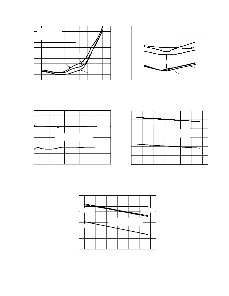
TYPICAL CHARACTERISTICS
35
-60
-40
15
2170 MHz
P
out
, OUTPUT POWER (dBm)
Figure 9. W-CDMA ACPR versus Output Power
ACPR,
ADJACENT
CHANNEL
POWER RA
TIO
(dBc)
V
DD
= 27 Vdc
3GPP Test Model 1
64 DPCH
2110 MHz
2140 MHz
17
19
21
23
25
27
29
31
33
-42
-44
-46
-48
-50
-52
-54
-56
-58
2300
-70
-40
2000
I
DQ3
= 100 mA
122 mA
f, FREQUENCY (MHz)
Figure 10. Two-Tone IMR versus Frequency
IMR (dBc)
V
DD
= 27 Vdc
P
out
= 23 dBm Two-Tone Avg.
Tone Spacing = 100 kHz
2250
2200
2150
2100
2050
-45
-50
-55
-60
-65
100 mA
122 mA
111 mA
3rd Order
5th Order
25
-70
-50
0
3rd Order
TONE SPACING (MHz)
Figure 11. Two-Tone Broadband Performance
INTERMODULA
TION DIST
ORTION
(dBc)
IMD,
V
DD
= 27 Vdc, f = 2140
P
out
= 23 dBm, Two-Tone Avg.
5th Order
-52
-54
-56
-58
-60
-62
-64
-66
-68
5
10
15
20
100
3.00
6.00
-40
T, TEMPERATURE (C)
Figure 12. Fixture Bias versus Temperature
V
DD
= 27 Vdc
R1 = R2 = R3 = 1000 Ohms
-30 -20 -10
0
10
20
30
40
50
60 70
80 90
5.75
5.50
5.25
5.00
4.75
4.50
4.25
4.00
3.75
3.50
3.25
V
bias
, FIXTURE BIAS VOL
T
AGE
(V)
V
BIAS3
T, TEMPERATURE (C)
Figure 13. Gate Bias versus Temperature
100
3.20
4.20
-40
V
gs1
& V
gs2
V
DD
= 27 Vdc
R1 = R2 = R3 = 1000 Ohms
-30 -20 -10
0
10 20
30
40
50
60 70
80 90
4.10
4.00
3.90
3.80
3.70
3.60
3.50
3.40
3.30
V
gs
, IC GA
TE
BIAS
VOL
T
AGE
(V)
V
gs3
0.00
2.00
1.80
1.60
1.40
1.20
1.00
0.80
0.60
0.40
0.20
I
gs
,
GA
TE BIAS CURRENT (mA)
I
gs1
& I
gs2
I
gs3
V
BIAS1
V
BIAS2
F
r
e
e
s
c
a
l
e
S
e
m
i
c
o
n
d
u
c
t
o
r
,
I
Freescale Semiconductor, Inc.
For More Information On This Product,
Go to: www.freescale.com
n
c
.
.
.