Äîêóìåíòàöèÿ è îïèñàíèÿ www.docs.chipfind.ru
1
MHVIC915R2
MOTOROLA RF DEVICE DATA
The RF Line
746-960 MHz RF LDMOS Wideband
Integrated Power Amplifier
The MHVIC915R2 wideband integrated circuit is designed for CDMA and
GSM/GSM EDGE applications. It uses Motorola's newest high voltage (26
to 28 Volts) LDMOS IC technology and integrates a multistage structure.
Its wideband OnChip integral matching circuitry makes it usable from 746
to 960 MHz. The linearity performances cover all modulations for cellular
applications: GSM, GSM EDGE, TDMA, and CDMA. The device is
packaged in a PFP16 flat pack package that provides excellent thermal
performance through a solderable backside contact.
· Typical CDMA Performance: 869894 MHz, 27 Volts, I
DQ1
= 80 mA, I
DQ2
=
120 mA, 1Carrier NCDMA, IS95 CDMA 9Channel Forward
Driver Application
Output Power -- 23 dBm
Power Gain -- 31 dB
Adjacent Channel Power Ratio --
60 dBc @ 750 kHz in a 30 kHz BW
66 dBc @ 1.98 MHz in a 30 kHz BW
Output Application
Output Power -- 34 dBm
PAE = 21%
Adjacent Channel Power Ratio --
50 dBc @ 750 kHz in a 30 kHz BW
· Typical GSM Performance: 921960 MHz, 26 Volts
Output Power -- 15 W P1dB
Power Gain -- 30 dB @ P1dB
Drain Efficiency = 56% @ P1dB
· OnChip Matching (50 Ohm Input, >9 Ohm Output)
· OnChip Current Mirror g
m
Sensing FET for Self Bias Application
· Integrated Temperature Compensation Capability
· Usable for SCPA and MCPA Architecture
· Integrated ESD Protection
· Available in Tape and Reel. R2 Suffix = 1,500 Units per 16 mm, 13 inch
Reel.
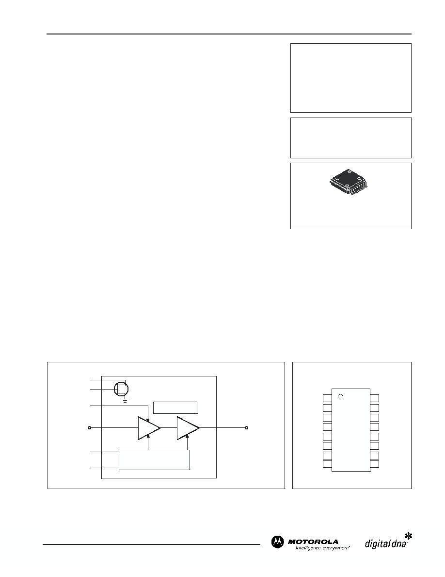
PIN CONNECTIONS
16
15
14
13
12
11
10
1
2
3
4
5
6
7
8
(Top View)
9
N.C.
V
D1
Gnd
V
G1
V
G2
N.C.
V
D2
/RF
out
V
D2
/RF
out
V
D2
/RF
out
V
D2
/RF
out
V
D2
/RF
out
V
D2
/RF
out
N.C.
V
G1
RF
in
IC
V
D1
V
G2
RF
in
V
D2
/RF
out
2 Stage IC
Temperature Compensation
V
BSD
V
BSG
V
BSD
V
BSG
Order this document
by MHVIC915R2/D
MOTOROLA
SEMICONDUCTOR TECHNICAL DATA
MHVIC915R2
CASE 97803
PFP16
PLASTIC
CDMA, GSM/GSM EDGE
746960 MHz, 15 W, 27 V
RF LDMOS WIDEBAND
INTEGRATED AMPLIFIER
Motorola, Inc. 2003
REV 3
F
r
e
e
s
c
a
l
e
S
e
m
i
c
o
n
d
u
c
t
o
r
,
I
Freescale Semiconductor, Inc.
For More Information On This Product,
Go to: www.freescale.com
n
c
.
.
.
MHVIC915R2
2
MOTOROLA RF DEVICE DATA
MAXIMUM RATINGS
Rating
Symbol
Value
Unit
DrainSource Voltage
V
DSS
65
Vdc
GateSource Voltage
V
GS
0.5, +15
Vdc
Storage Temperature Range
T
stg
65 to +150
°C
Operating Junction Temperature
T
J
150
°C
THERMAL CHARACTERISTICS
Characteristic
Symbol
Max
Unit
Thermal Resistance, Junction to Case
Driver Application
Stage 1, 27 Vdc, I
DQ
= 80 mA
(P
out
= 0.2 W CW)
Stage 2, 27 Vdc, I
DQ
= 120 mA
Output Application
Stage 1, 27 Vdc, I
DQ
= 80 mA
(P
out
= 2.5 W CW)
Stage 2, 27 Vdc, I
DQ
= 120 mA
GSM Application
Stage 1, 26 Vdc, I
DQ
= 50 mA
(P
out
= 15 W CW)
Stage 2, 26 Vdc, I
DQ
= 140 mA
R
JC
5.07
3.73
3.41
°C/W
ESD PROTECTION CHARACTERISTICS
Test Conditions
Class
Human Body Model
1 (Minimum)
Machine Model
M1 (Minimum)
Charge Device Model
C4 (Minimum)
MOISTURE SENSITIVITY LEVEL
Test Methodology
Rating
Per JESD 22A113
3
ELECTRICAL CHARACTERISTICS
(T
C
= 25
°C unless otherwise noted)
Characteristic
Symbol
Min
Typ
Max
Unit
CDMA FUNCTIONAL TESTS (In Motorola CDMA Test Fixture, 50
hm system) V
DS
= 27 V, I
DQ1
= 80 mA, I
DQ2
= 120 mA, 880 MHz,
1Carrier NCDMA, IS95 CDMA 9Channel Forward
CommonSource Amplifier Power Gain (P
out
= 23 dBm)
G
ps
29
31
--
dB
Power Added Efficiency (P
out
= 34 dBm)
--
21
--
%
Input Return Loss (P
out
= 23 dBm)
IRL
--
12
9
dB
Adjacent Channel Power Ratio (P
out
= 23 dBm) @ 750 kHz offset in 30 kHz BW
ACPR
--
60
55
dBc
Adjacent Channel Power Ratio (P
out
= 34 dBm) @ 750 kHz offset in 30 kHz BW
ACPR
--
50
--
dBc
Gain Flatness @ P
out
= 23 dBm (865 MHz to 895 MHz)
G
F
--
0.2
0.4
dB
Bias Sense FET Drain Current
V
BSD
= 27 V
V
BIAS
BSG
= V
BIAS2 Q2
@ I
DQ2
= 120 mA
I
BSD
0.8
1.2
1.6
mA
(continued)
F
r
e
e
s
c
a
l
e
S
e
m
i
c
o
n
d
u
c
t
o
r
,
I
Freescale Semiconductor, Inc.
For More Information On This Product,
Go to: www.freescale.com
n
c
.
.
.
3
MHVIC915R2
MOTOROLA RF DEVICE DATA
ELECTRICAL CHARACTERISTICS continued
(T
C
= 25
°C unless otherwise noted)
Characteristic
Symbol
Min
Typ
Max
Unit
PERFORMANCE TESTS (In Motorola Test Fixture, 50
hm system) V
DS
= 27 V, I
DQ1
= 80 mA, I
DQ2
= 120 mA, 865895 MHz
Rating
Symbol
Min
Typ
Max
Unit
Quiescent Current Accuracy over Temperature (10 to 85
°C) at Nominal Value
Iqt
--
±5
--
%
Gain Flatness @ P
out
= 23 dBm (800 MHz to 960 MHz)
G
F
--
0.20
--
dB
Deviation from Linear Phase @ P
out
= 23 dBm
--
±0.2
--
°
Group Delay @ P
out
= 23 dBm
Delay
--
2.2
--
ns
Insertion Phase Window @ P
out
= 23 dBm (part to part)
--
±10
--
°
GSM FUNCTIONAL TESTS (In Motorola GSM Test Fixture, 50
hm system) V
DS
= 26 V, I
DQ1
= 50 mA, I
DQ2
= 140 mA, 921960 MHz, CW
Rating
Symbol
Min
Typ
Max
Unit
Output Power at 1dB Compression Point
P1dB
--
15
--
Watts
CommonSource Amplifier Power Gain @ P1dB
Gain
--
30
--
dB
Drain Efficiency @ P1dB
--
56
--
%
Input return Loss @ P1dB
IRL
--
16
--
dB
EVM @ 5 W
--
--
0.9
--
%
Third Order Intermodulation Distortion (15 W PEP, 2 Tone 100 kHz spacing)
IMD3
--
30
--
dBc
Drain Efficiency (15 W PEP, 2 Tone 100 kHz spacing)
--
35
--
%
F
r
e
e
s
c
a
l
e
S
e
m
i
c
o
n
d
u
c
t
o
r
,
I
Freescale Semiconductor, Inc.
For More Information On This Product,
Go to: www.freescale.com
n
c
.
.
.
MHVIC915R2
4
MOTOROLA RF DEVICE DATA
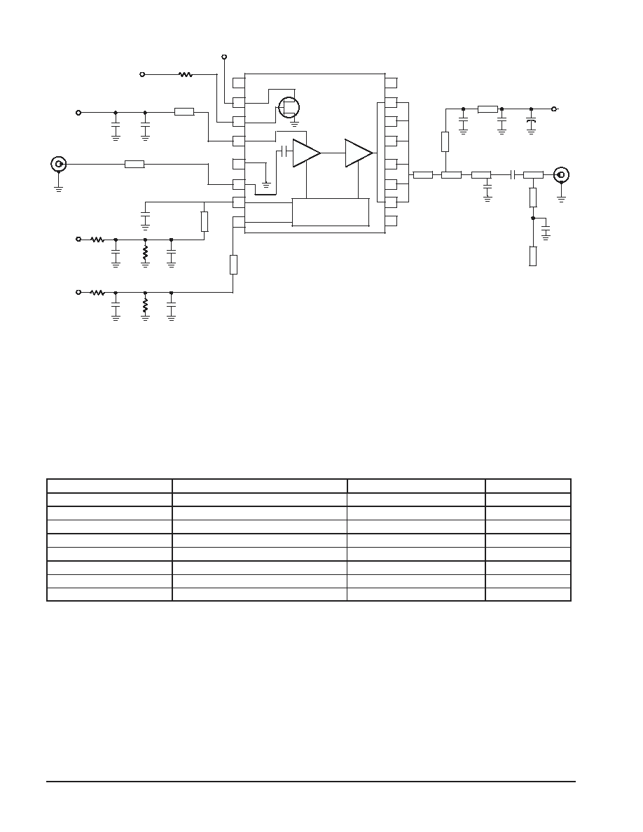
9
Z7
0.0504
x 0.480 Microstrip
Z8
0.0252
x 0.843 Microstrip
Z9
0.0252
x 0.167 Microstrip
Z10
0.040
x 0.850 Microstrip
Z11
0.025
x 0.400 Microstrip
Z12
0.020
x 0.710 Microstrip
PCB
Rogers 4350, 0.020
,
r
= 3.50
Figure 1. MHVIC915 746960 MHz Test Circuit Schematic
Z1
0.0438
x 0.400 50 Microstrip
Z2
0.1709
x 0.1004 Microstrip
(not including IC pad length)
Z3
0.1222
x 0.1944 Microstrip
Z4
0.0836
x 0.3561 Microstrip
Z5
0.0438
x 0.2725 Microstrip
Z6
0.0504
x 0.3378 Microstrip
RF
OUTPUT
RF
INPUT
Z1
V
D2
Z7
Z6
C4
C6
Z2
Z3
Z4
Z5
Z8
Z9
C2
C3
C1
V
BIAS2
R2
R4
C10
C9
V
D1
C8
C7
1
2
3
4
5
6
7
8
10
16
NC
NC
NC
14
15
12
13
11
Temperature
Compensation
+
C5
Z10
V
GS2
V
BIAS1
R1
R3
C11
C12
Z12
V
GS1
C13
Z11
V
BIAS BSG
R5
V
BSD
Table 1. MHVIC915 746960 MHz Test Circuit Component Designations and Values
Part
Description
Value, P/N or DWG
Manufacturer
C1, C2
4.7 pF High Q Capacitors (0603)
ATC600S4R7CW
ATC
C3, C4
47 pF NPO Capacitors (0805)
GRM40001COG470J050BD
Murata
C5, C8, C10, C11
1
µF X7R Chip Capacitors (1214)
GRM422X7R105K050AL
Murata
C6
10
µF, 50 V Electrolytic Capacitor
ECEV1HA100SP
Panasonic
C7, C9, C12
0.01
µF X7R Chip Capacitors (0805)
GRM40X7R103J050BD
Murata
C13
8.2 pF NPO Chip Capacitor (0805)
GRM40001COG8R2C050BD
Murata
R1, R2, R5
1 k
W Chip Resistors (0603)
RM73B2AT102J
KOA Speer
R3, R4
100 k
W Chip Resistors (0603)
RM73B2AT104J
KOA Speer
F
r
e
e
s
c
a
l
e
S
e
m
i
c
o
n
d
u
c
t
o
r
,
I
Freescale Semiconductor, Inc.
For More Information On This Product,
Go to: www.freescale.com
n
c
.
.
.
5
MHVIC915R2
MOTOROLA RF DEVICE DATA
V
BIAS BSG
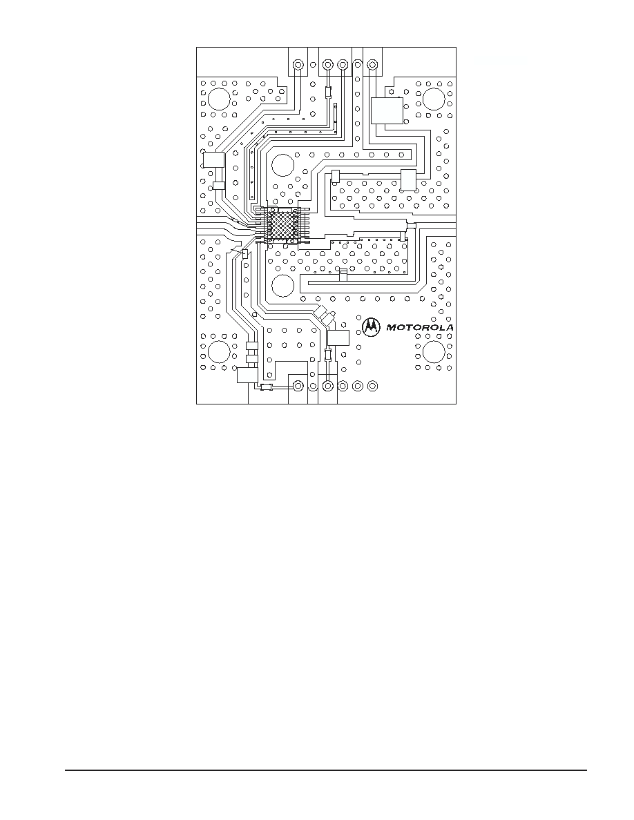
Figure 2. MHVIC915 746960 MHz Test Circuit Component Layout
Rev 0
MHVIC915
V
D1
V
D2
V
BIAS1
V
BIAS2
C10
C11
C12
R3
R2
R1
R4
C9
C3
C2
C1
C13
C4
C5
C6
C8
C7
R5
V
BSD
F
r
e
e
s
c
a
l
e
S
e
m
i
c
o
n
d
u
c
t
o
r
,
I
Freescale Semiconductor, Inc.
For More Information On This Product,
Go to: www.freescale.com
n
c
.
.
.