 | ÐлекÑÑоннÑй компоненÑ: MJD1121 | СкаÑаÑÑ:  PDF PDF  ZIP ZIP |
Äîêóìåíòàöèÿ è îïèñàíèÿ www.docs.chipfind.ru
1
Motorola Bipolar Power Transistor Device Data
Complementary Darlington
Power Transistors
DPAK For Surface Mount Applications
Designed for general purpose power and switching such as output or driver stages
in applications such as switching regulators, converters, and power amplifiers.
·
Lead Formed for Surface Mount Applications in Plastic Sleeves (No Suffix)
·
Straight Lead Version in Plastic Sleeves ("1" Suffix)
·
Lead Formed Version in 16 mm Tape and Reel ("T4" Suffix)
·
Surface Mount Replacements for TIP110TIP117 Series
·
Monolithic Construction With Builtin BaseEmitter Shunt Resistors
·
High DC Current Gain -- hFE = 2500 (Typ) @ IC = 2.0 Adc
·
Complementary Pairs Simplifies Designs
ÎÎÎÎÎÎÎÎÎÎÎÎÎÎÎÎÎÎÎÎÎÎÎ
ÎÎÎÎÎÎÎÎÎÎÎÎÎÎÎÎÎÎÎÎÎÎÎ
ÎÎÎÎÎÎÎÎÎÎÎÎÎÎÎÎÎÎÎÎÎÎÎ
ÎÎÎÎÎÎÎÎÎÎÎÎÎÎÎÎÎÎÎÎÎÎÎ
MAXIMUM RATINGS
ÎÎÎÎÎÎÎÎÎÎÎÎÎ
ÎÎÎÎÎÎÎÎÎÎÎÎÎ
ÎÎÎÎÎÎÎÎÎÎÎÎÎ
ÎÎÎÎÎÎÎÎÎÎÎÎÎ
ÎÎÎÎÎÎÎÎÎÎÎÎÎ
Rating
ÎÎÎÎ
ÎÎÎÎ
ÎÎÎÎ
ÎÎÎÎ
ÎÎÎÎ
Symbol
ÎÎÎÎÎÎ
ÎÎÎÎÎÎ
ÎÎÎÎÎÎ
ÎÎÎÎÎÎ
ÎÎÎÎÎÎ
MJD112
MJD117
ÎÎÎ
ÎÎÎ
ÎÎÎ
ÎÎÎ
ÎÎÎ
Unit
ÎÎÎÎÎÎÎÎÎÎÎÎÎ
ÎÎÎÎÎÎÎÎÎÎÎÎÎ
ÎÎÎÎÎÎÎÎÎÎÎÎÎ
ÎÎÎÎÎÎÎÎÎÎÎÎÎ
CollectorEmitter Voltage
ÎÎÎÎ
ÎÎÎÎ
ÎÎÎÎ
ÎÎÎÎ
VCEO
ÎÎÎÎÎÎ
ÎÎÎÎÎÎ
ÎÎÎÎÎÎ
ÎÎÎÎÎÎ
100
ÎÎÎ
ÎÎÎ
ÎÎÎ
ÎÎÎ
Vdc
ÎÎÎÎÎÎÎÎÎÎÎÎÎ
ÎÎÎÎÎÎÎÎÎÎÎÎÎ
ÎÎÎÎÎÎÎÎÎÎÎÎÎ
ÎÎÎÎÎÎÎÎÎÎÎÎÎ
CollectorBase Voltage
ÎÎÎÎ
ÎÎÎÎ
ÎÎÎÎ
ÎÎÎÎ
VCB
ÎÎÎÎÎÎ
ÎÎÎÎÎÎ
ÎÎÎÎÎÎ
ÎÎÎÎÎÎ
100
ÎÎÎ
ÎÎÎ
ÎÎÎ
ÎÎÎ
Vdc
ÎÎÎÎÎÎÎÎÎÎÎÎÎ
ÎÎÎÎÎÎÎÎÎÎÎÎÎ
ÎÎÎÎÎÎÎÎÎÎÎÎÎ
ÎÎÎÎÎÎÎÎÎÎÎÎÎ
EmitterBase Voltage
ÎÎÎÎ
ÎÎÎÎ
ÎÎÎÎ
ÎÎÎÎ
VEB
ÎÎÎÎÎÎ
ÎÎÎÎÎÎ
ÎÎÎÎÎÎ
ÎÎÎÎÎÎ
5
ÎÎÎ
ÎÎÎ
ÎÎÎ
ÎÎÎ
Vdc
ÎÎÎÎÎÎÎÎÎÎÎÎÎ
ÎÎÎÎÎÎÎÎÎÎÎÎÎ
ÎÎÎÎÎÎÎÎÎÎÎÎÎ
ÎÎÎÎÎÎÎÎÎÎÎÎÎ
Collector Current -- Continuous
Peak
ÎÎÎÎ
ÎÎÎÎ
ÎÎÎÎ
ÎÎÎÎ
IC
ÎÎÎÎÎÎ
ÎÎÎÎÎÎ
ÎÎÎÎÎÎ
ÎÎÎÎÎÎ
2
4
ÎÎÎ
ÎÎÎ
ÎÎÎ
ÎÎÎ
Adc
ÎÎÎÎÎÎÎÎÎÎÎÎÎ
ÎÎÎÎÎÎÎÎÎÎÎÎÎ
ÎÎÎÎÎÎÎÎÎÎÎÎÎ
ÎÎÎÎÎÎÎÎÎÎÎÎÎ
Base Current
ÎÎÎÎ
ÎÎÎÎ
ÎÎÎÎ
ÎÎÎÎ
IB
ÎÎÎÎÎÎ
ÎÎÎÎÎÎ
ÎÎÎÎÎÎ
ÎÎÎÎÎÎ
50
ÎÎÎ
ÎÎÎ
ÎÎÎ
ÎÎÎ
mAdc
ÎÎÎÎÎÎÎÎÎÎÎÎÎ
ÎÎÎÎÎÎÎÎÎÎÎÎÎ
ÎÎÎÎÎÎÎÎÎÎÎÎÎ
ÎÎÎÎÎÎÎÎÎÎÎÎÎ
ÎÎÎÎÎÎÎÎÎÎÎÎÎ
Total Power Dissipation @ TC = 25
_
C
Derate above 25
_
C
ÎÎÎÎ
ÎÎÎÎ
ÎÎÎÎ
ÎÎÎÎ
ÎÎÎÎ
PD
ÎÎÎÎÎÎ
ÎÎÎÎÎÎ
ÎÎÎÎÎÎ
ÎÎÎÎÎÎ
ÎÎÎÎÎÎ
20
0.16
ÎÎÎ
ÎÎÎ
ÎÎÎ
ÎÎÎ
ÎÎÎ
Watts
W/
_
C
ÎÎÎÎÎÎÎÎÎÎÎÎÎ
ÎÎÎÎÎÎÎÎÎÎÎÎÎ
ÎÎÎÎÎÎÎÎÎÎÎÎÎ
ÎÎÎÎÎÎÎÎÎÎÎÎÎ
Total Power Dissipation* @ TA = 25
_
C
Derate above 25
_
C
ÎÎÎÎ
ÎÎÎÎ
ÎÎÎÎ
ÎÎÎÎ
PD
ÎÎÎÎÎÎ
ÎÎÎÎÎÎ
ÎÎÎÎÎÎ
ÎÎÎÎÎÎ
1.75
0.014
ÎÎÎ
ÎÎÎ
ÎÎÎ
ÎÎÎ
Watts
W/
_
C
ÎÎÎÎÎÎÎÎÎÎÎÎÎ
ÎÎÎÎÎÎÎÎÎÎÎÎÎ
ÎÎÎÎÎÎÎÎÎÎÎÎÎ
ÎÎÎÎÎÎÎÎÎÎÎÎÎ
ÎÎÎÎÎÎÎÎÎÎÎÎÎ
Operating and Storage Junction
Temperature Range
ÎÎÎÎ
ÎÎÎÎ
ÎÎÎÎ
ÎÎÎÎ
ÎÎÎÎ
TJ, Tstg
ÎÎÎÎÎÎ
ÎÎÎÎÎÎ
ÎÎÎÎÎÎ
ÎÎÎÎÎÎ
ÎÎÎÎÎÎ
65 to + 150
ÎÎÎ
ÎÎÎ
ÎÎÎ
ÎÎÎ
ÎÎÎ
_
C
ÎÎÎÎÎÎÎÎÎÎÎÎÎÎÎÎÎÎÎÎÎÎÎ
ÎÎÎÎÎÎÎÎÎÎÎÎÎÎÎÎÎÎÎÎÎÎÎ
ÎÎÎÎÎÎÎÎÎÎÎÎÎÎÎÎÎÎÎÎÎÎÎ
ÎÎÎÎÎÎÎÎÎÎÎÎÎÎÎÎÎÎÎÎÎÎÎ
THERMAL CHARACTERISTICS
ÎÎÎÎÎÎÎÎÎÎÎÎÎ
ÎÎÎÎÎÎÎÎÎÎÎÎÎ
ÎÎÎÎÎÎÎÎÎÎÎÎÎ
ÎÎÎÎÎÎÎÎÎÎÎÎÎ
Characteristic
ÎÎÎÎ
ÎÎÎÎ
ÎÎÎÎ
ÎÎÎÎ
Symbol
ÎÎÎÎÎÎ
ÎÎÎÎÎÎ
ÎÎÎÎÎÎ
ÎÎÎÎÎÎ
Max
ÎÎÎ
ÎÎÎ
ÎÎÎ
ÎÎÎ
Unit
ÎÎÎÎÎÎÎÎÎÎÎÎÎ
ÎÎÎÎÎÎÎÎÎÎÎÎÎ
ÎÎÎÎÎÎÎÎÎÎÎÎÎ
ÎÎÎÎÎÎÎÎÎÎÎÎÎ
Thermal Resistance, Junction to Case
ÎÎÎÎ
ÎÎÎÎ
ÎÎÎÎ
ÎÎÎÎ
R
JC
ÎÎÎÎÎÎ
ÎÎÎÎÎÎ
ÎÎÎÎÎÎ
ÎÎÎÎÎÎ
6.25
ÎÎÎ
ÎÎÎ
ÎÎÎ
ÎÎÎ
_
C/W
ÎÎÎÎÎÎÎÎÎÎÎÎÎ
ÎÎÎÎÎÎÎÎÎÎÎÎÎ
ÎÎÎÎÎÎÎÎÎÎÎÎÎ
ÎÎÎÎÎÎÎÎÎÎÎÎÎ
Thermal Resistance, Junction to Ambient*
ÎÎÎÎ
ÎÎÎÎ
ÎÎÎÎ
ÎÎÎÎ
R
JA
ÎÎÎÎÎÎ
ÎÎÎÎÎÎ
ÎÎÎÎÎÎ
ÎÎÎÎÎÎ
71.4
ÎÎÎ
ÎÎÎ
ÎÎÎ
ÎÎÎ
_
C/W
ÎÎÎÎÎÎÎÎÎÎÎÎÎÎÎÎÎÎÎÎÎÎÎ
ÎÎÎÎÎÎÎÎÎÎÎÎÎÎÎÎÎÎÎÎÎÎÎ
ÎÎÎÎÎÎÎÎÎÎÎÎÎÎÎÎÎÎÎÎÎÎÎ
ÎÎÎÎÎÎÎÎÎÎÎÎÎÎÎÎÎÎÎÎÎÎÎ
ELECTRICAL CHARACTERISTICS
(TC = 25
_
C unless otherwise noted)
ÎÎÎÎÎÎÎÎÎÎÎÎÎ
ÎÎÎÎÎÎÎÎÎÎÎÎÎ
ÎÎÎÎÎÎÎÎÎÎÎÎÎ
ÎÎÎÎÎÎÎÎÎÎÎÎÎ
Characteristic
ÎÎÎÎ
ÎÎÎÎ
ÎÎÎÎ
ÎÎÎÎ
Symbol
ÎÎÎÎ
ÎÎÎÎ
ÎÎÎÎ
ÎÎÎÎ
Min
ÎÎÎ
ÎÎÎ
ÎÎÎ
ÎÎÎ
Max
ÎÎÎ
ÎÎÎ
ÎÎÎ
ÎÎÎ
Unit
ÎÎÎÎÎÎÎÎÎÎÎÎÎÎÎÎÎÎÎÎÎÎÎ
ÎÎÎÎÎÎÎÎÎÎÎÎÎÎÎÎÎÎÎÎÎÎÎ
ÎÎÎÎÎÎÎÎÎÎÎÎÎÎÎÎÎÎÎÎÎÎÎ
ÎÎÎÎÎÎÎÎÎÎÎÎÎÎÎÎÎÎÎÎÎÎÎ
OFF CHARACTERISTICS
ÎÎÎÎÎÎÎÎÎÎÎÎÎ
ÎÎÎÎÎÎÎÎÎÎÎÎÎ
ÎÎÎÎÎÎÎÎÎÎÎÎÎ
ÎÎÎÎÎÎÎÎÎÎÎÎÎ
ÎÎÎÎÎÎÎÎÎÎÎÎÎ
CollectorEmitter Sustaining Voltage (1)
(IC = 30 mAdc, IB = 0)
ÎÎÎÎ
ÎÎÎÎ
ÎÎÎÎ
ÎÎÎÎ
ÎÎÎÎ
VCEO(sus)
ÎÎÎÎ
ÎÎÎÎ
ÎÎÎÎ
ÎÎÎÎ
ÎÎÎÎ
100
ÎÎÎ
ÎÎÎ
ÎÎÎ
ÎÎÎ
ÎÎÎ
--
ÎÎÎ
ÎÎÎ
ÎÎÎ
ÎÎÎ
ÎÎÎ
Vdc
ÎÎÎÎÎÎÎÎÎÎÎÎÎ
ÎÎÎÎÎÎÎÎÎÎÎÎÎ
ÎÎÎÎÎÎÎÎÎÎÎÎÎ
ÎÎÎÎÎÎÎÎÎÎÎÎÎ
Collector Cutoff Current
(VCE = 50 Vdc, IB = 0)
ÎÎÎÎ
ÎÎÎÎ
ÎÎÎÎ
ÎÎÎÎ
ICEO
ÎÎÎÎ
ÎÎÎÎ
ÎÎÎÎ
ÎÎÎÎ
--
ÎÎÎ
ÎÎÎ
ÎÎÎ
ÎÎÎ
20
ÎÎÎ
ÎÎÎ
ÎÎÎ
ÎÎÎ
µ
Adc
ÎÎÎÎÎÎÎÎÎÎÎÎÎ
ÎÎÎÎÎÎÎÎÎÎÎÎÎ
ÎÎÎÎÎÎÎÎÎÎÎÎÎ
ÎÎÎÎÎÎÎÎÎÎÎÎÎ
ÎÎÎÎÎÎÎÎÎÎÎÎÎ
Collector Cutoff Current
(VCB = 100 Vdc, IE = 0)
ÎÎÎÎ
ÎÎÎÎ
ÎÎÎÎ
ÎÎÎÎ
ÎÎÎÎ
ICBO
ÎÎÎÎ
ÎÎÎÎ
ÎÎÎÎ
ÎÎÎÎ
ÎÎÎÎ
--
ÎÎÎ
ÎÎÎ
ÎÎÎ
ÎÎÎ
ÎÎÎ
20
ÎÎÎ
ÎÎÎ
ÎÎÎ
ÎÎÎ
ÎÎÎ
µ
Adc
ÎÎÎÎÎÎÎÎÎÎÎÎÎ
ÎÎÎÎÎÎÎÎÎÎÎÎÎ
ÎÎÎÎÎÎÎÎÎÎÎÎÎ
ÎÎÎÎÎÎÎÎÎÎÎÎÎ
ÎÎÎÎÎÎÎÎÎÎÎÎÎ
Emitter Cutoff Current
(VBE = 5 Vdc, IC = 0)
ÎÎÎÎ
ÎÎÎÎ
ÎÎÎÎ
ÎÎÎÎ
ÎÎÎÎ
IEBO
ÎÎÎÎ
ÎÎÎÎ
ÎÎÎÎ
ÎÎÎÎ
ÎÎÎÎ
--
ÎÎÎ
ÎÎÎ
ÎÎÎ
ÎÎÎ
ÎÎÎ
2
ÎÎÎ
ÎÎÎ
ÎÎÎ
ÎÎÎ
ÎÎÎ
mAdc
* These ratings are applicable when surface mounted on the minimum pad sizes recommended.
(1) Pulse Test: Pulse Width
v
300
µ
s, Duty Cycle
v
2%.
(continued)
Preferred devices are Motorola recommended choices for future use and best overall value.
MOTOROLA
SEMICONDUCTOR TECHNICAL DATA
Order this document
by MJD112/D
©
Motorola, Inc. 1995
MJD112
MJD117
CASE 369A13
SILICON
POWER TRANSISTORS
2 AMPERES
100 VOLTS
20 WATTS
*Motorola Preferred Device
CASE 36907
MINIMUM PAD SIZES
RECOMMENDED FOR
SURFACE MOUNTED
APPLICATIONS
0.243
6.172
0.063
1.6
0.1
18
3.0
0.07
1.8
0.165
4.191
0.190
4.826
inches
mm
*
NPN
PNP
*
REV 1
MJD112 MJD117
2
Motorola Bipolar Power Transistor Device Data
ÎÎÎÎÎÎÎÎÎÎÎÎÎÎÎÎÎÎÎÎÎÎÎÎÎÎÎÎÎÎÎÎÎÎ
ÎÎÎÎÎÎÎÎÎÎÎÎÎÎÎÎÎÎÎÎÎÎÎÎÎÎÎÎÎÎÎÎÎÎ
ÎÎÎÎÎÎÎÎÎÎÎÎÎÎÎÎÎÎÎÎÎÎÎÎÎÎÎÎÎÎÎÎÎÎ
ÎÎÎÎÎÎÎÎÎÎÎÎÎÎÎÎÎÎÎÎÎÎÎÎÎÎÎÎÎÎÎÎÎÎ
*ELECTRICAL CHARACTERISTICS -- continued
(TC = 25
_
C unless otherwise noted)
ÎÎÎÎÎÎÎÎÎÎÎÎÎÎÎÎÎÎÎÎÎÎÎ
ÎÎÎÎÎÎÎÎÎÎÎÎÎÎÎÎÎÎÎÎÎÎÎ
ÎÎÎÎÎÎÎÎÎÎÎÎÎÎÎÎÎÎÎÎÎÎÎ
ÎÎÎÎÎÎÎÎÎÎÎÎÎÎÎÎÎÎÎÎÎÎÎ
Characteristic
ÎÎÎÎ
ÎÎÎÎ
ÎÎÎÎ
ÎÎÎÎ
Symbol
ÎÎÎÎ
ÎÎÎÎ
ÎÎÎÎ
ÎÎÎÎ
Min
ÎÎÎÎ
ÎÎÎÎ
ÎÎÎÎ
ÎÎÎÎ
Max
ÎÎÎ
ÎÎÎ
ÎÎÎ
ÎÎÎ
Unit
ÎÎÎÎÎÎÎÎÎÎÎÎÎÎÎÎÎÎÎÎÎÎÎÎÎÎÎÎÎÎÎÎÎÎ
ÎÎÎÎÎÎÎÎÎÎÎÎÎÎÎÎÎÎÎÎÎÎÎÎÎÎÎÎÎÎÎÎÎÎ
ÎÎÎÎÎÎÎÎÎÎÎÎÎÎÎÎÎÎÎÎÎÎÎÎÎÎÎÎÎÎÎÎÎÎ
ÎÎÎÎÎÎÎÎÎÎÎÎÎÎÎÎÎÎÎÎÎÎÎÎÎÎÎÎÎÎÎÎÎÎ
OFF CHARACTERISTICS continued
ÎÎÎÎÎÎÎÎÎÎÎÎÎÎÎÎÎÎÎÎÎÎÎ
ÎÎÎÎÎÎÎÎÎÎÎÎÎÎÎÎÎÎÎÎÎÎÎ
ÎÎÎÎÎÎÎÎÎÎÎÎÎÎÎÎÎÎÎÎÎÎÎ
ÎÎÎÎÎÎÎÎÎÎÎÎÎÎÎÎÎÎÎÎÎÎÎ
ÎÎÎÎÎÎÎÎÎÎÎÎÎÎÎÎÎÎÎÎÎÎÎ
ÎÎÎÎÎÎÎÎÎÎÎÎÎÎÎÎÎÎÎÎÎÎÎ
CollectorCutoff Current
(VCE = 80 Vdc, VBE(off) = 1.5 Vdc)
(VCE = 80 Vdc, VBE(off) = 1.5 Vdc, TC = 125
_
C)
ÎÎÎÎ
ÎÎÎÎ
ÎÎÎÎ
ÎÎÎÎ
ÎÎÎÎ
ÎÎÎÎ
ICEX
ÎÎÎÎ
ÎÎÎÎ
ÎÎÎÎ
ÎÎÎÎ
ÎÎÎÎ
ÎÎÎÎ
--
--
ÎÎÎÎ
ÎÎÎÎ
ÎÎÎÎ
ÎÎÎÎ
ÎÎÎÎ
ÎÎÎÎ
10
500
ÎÎÎ
ÎÎÎ
ÎÎÎ
ÎÎÎ
ÎÎÎ
ÎÎÎ
µ
Adc
ÎÎÎÎÎÎÎÎÎÎÎÎÎÎÎÎÎÎÎÎÎÎÎ
ÎÎÎÎÎÎÎÎÎÎÎÎÎÎÎÎÎÎÎÎÎÎÎ
ÎÎÎÎÎÎÎÎÎÎÎÎÎÎÎÎÎÎÎÎÎÎÎ
ÎÎÎÎÎÎÎÎÎÎÎÎÎÎÎÎÎÎÎÎÎÎÎ
CollectorCutoff Current (VCB = 80 Vdc, IE = 0)
ÎÎÎÎ
ÎÎÎÎ
ÎÎÎÎ
ÎÎÎÎ
ICBO
ÎÎÎÎ
ÎÎÎÎ
ÎÎÎÎ
ÎÎÎÎ
--
ÎÎÎÎ
ÎÎÎÎ
ÎÎÎÎ
ÎÎÎÎ
10
ÎÎÎ
ÎÎÎ
ÎÎÎ
ÎÎÎ
µ
Adc
ÎÎÎÎÎÎÎÎÎÎÎÎÎÎÎÎÎÎÎÎÎÎÎ
ÎÎÎÎÎÎÎÎÎÎÎÎÎÎÎÎÎÎÎÎÎÎÎ
ÎÎÎÎÎÎÎÎÎÎÎÎÎÎÎÎÎÎÎÎÎÎÎ
ÎÎÎÎÎÎÎÎÎÎÎÎÎÎÎÎÎÎÎÎÎÎÎ
EmitterCutoff Current (VBE = 5 Vdc, IC = 0)
ÎÎÎÎ
ÎÎÎÎ
ÎÎÎÎ
ÎÎÎÎ
IEBO
ÎÎÎÎ
ÎÎÎÎ
ÎÎÎÎ
ÎÎÎÎ
--
ÎÎÎÎ
ÎÎÎÎ
ÎÎÎÎ
ÎÎÎÎ
2
ÎÎÎ
ÎÎÎ
ÎÎÎ
ÎÎÎ
mAdc
ÎÎÎÎÎÎÎÎÎÎÎÎÎÎÎÎÎÎÎÎÎÎÎÎÎÎÎÎÎÎÎÎÎÎ
ÎÎÎÎÎÎÎÎÎÎÎÎÎÎÎÎÎÎÎÎÎÎÎÎÎÎÎÎÎÎÎÎÎÎ
ÎÎÎÎÎÎÎÎÎÎÎÎÎÎÎÎÎÎÎÎÎÎÎÎÎÎÎÎÎÎÎÎÎÎ
ÎÎÎÎÎÎÎÎÎÎÎÎÎÎÎÎÎÎÎÎÎÎÎÎÎÎÎÎÎÎÎÎÎÎ
ON CHARACTERISTICS
ÎÎÎÎÎÎÎÎÎÎÎÎÎÎÎÎÎÎÎÎÎÎÎ
ÎÎÎÎÎÎÎÎÎÎÎÎÎÎÎÎÎÎÎÎÎÎÎ
ÎÎÎÎÎÎÎÎÎÎÎÎÎÎÎÎÎÎÎÎÎÎÎ
ÎÎÎÎÎÎÎÎÎÎÎÎÎÎÎÎÎÎÎÎÎÎÎ
ÎÎÎÎÎÎÎÎÎÎÎÎÎÎÎÎÎÎÎÎÎÎÎ
ÎÎÎÎÎÎÎÎÎÎÎÎÎÎÎÎÎÎÎÎÎÎÎ
DC Current Gain
(IC = 0.5 Adc, VCE = 3 Vdc)
(IC = 2 Adc, VCE = 3 Vdc)
(IC = 4 Adc, VCE = 3 Vdc)
ÎÎÎÎ
ÎÎÎÎ
ÎÎÎÎ
ÎÎÎÎ
ÎÎÎÎ
ÎÎÎÎ
hFE
ÎÎÎÎ
ÎÎÎÎ
ÎÎÎÎ
ÎÎÎÎ
ÎÎÎÎ
ÎÎÎÎ
500
1000
200
ÎÎÎÎ
ÎÎÎÎ
ÎÎÎÎ
ÎÎÎÎ
ÎÎÎÎ
ÎÎÎÎ
--
12,000
--
ÎÎÎ
ÎÎÎ
ÎÎÎ
ÎÎÎ
ÎÎÎ
ÎÎÎ
--
ÎÎÎÎÎÎÎÎÎÎÎÎÎÎÎÎÎÎÎÎÎÎÎ
ÎÎÎÎÎÎÎÎÎÎÎÎÎÎÎÎÎÎÎÎÎÎÎ
ÎÎÎÎÎÎÎÎÎÎÎÎÎÎÎÎÎÎÎÎÎÎÎ
ÎÎÎÎÎÎÎÎÎÎÎÎÎÎÎÎÎÎÎÎÎÎÎ
ÎÎÎÎÎÎÎÎÎÎÎÎÎÎÎÎÎÎÎÎÎÎÎ
ÎÎÎÎÎÎÎÎÎÎÎÎÎÎÎÎÎÎÎÎÎÎÎ
CollectorEmitter Saturation Voltage
(IC = 2 Adc, IB = 8 mAdc)
(IC = 4 Adc, IB = 40 mAdc)
ÎÎÎÎ
ÎÎÎÎ
ÎÎÎÎ
ÎÎÎÎ
ÎÎÎÎ
ÎÎÎÎ
VCE(sat)
ÎÎÎÎ
ÎÎÎÎ
ÎÎÎÎ
ÎÎÎÎ
ÎÎÎÎ
ÎÎÎÎ
--
--
ÎÎÎÎ
ÎÎÎÎ
ÎÎÎÎ
ÎÎÎÎ
ÎÎÎÎ
ÎÎÎÎ
2
3
ÎÎÎ
ÎÎÎ
ÎÎÎ
ÎÎÎ
ÎÎÎ
ÎÎÎ
Vdc
ÎÎÎÎÎÎÎÎÎÎÎÎÎÎÎÎÎÎÎÎÎÎÎ
ÎÎÎÎÎÎÎÎÎÎÎÎÎÎÎÎÎÎÎÎÎÎÎ
ÎÎÎÎÎÎÎÎÎÎÎÎÎÎÎÎÎÎÎÎÎÎÎ
ÎÎÎÎÎÎÎÎÎÎÎÎÎÎÎÎÎÎÎÎÎÎÎ
BaseEmitter Saturation Voltage (IC = 4 Adc, IB = 40 mAdc)
ÎÎÎÎ
ÎÎÎÎ
ÎÎÎÎ
ÎÎÎÎ
VBE(sat)
ÎÎÎÎ
ÎÎÎÎ
ÎÎÎÎ
ÎÎÎÎ
--
ÎÎÎÎ
ÎÎÎÎ
ÎÎÎÎ
ÎÎÎÎ
4
ÎÎÎ
ÎÎÎ
ÎÎÎ
ÎÎÎ
Vdc
ÎÎÎÎÎÎÎÎÎÎÎÎÎÎÎÎÎÎÎÎÎÎÎ
ÎÎÎÎÎÎÎÎÎÎÎÎÎÎÎÎÎÎÎÎÎÎÎ
ÎÎÎÎÎÎÎÎÎÎÎÎÎÎÎÎÎÎÎÎÎÎÎ
ÎÎÎÎÎÎÎÎÎÎÎÎÎÎÎÎÎÎÎÎÎÎÎ
BaseEmitter On Voltage (IC = 2 Adc, VCE = 3 Vdc)
ÎÎÎÎ
ÎÎÎÎ
ÎÎÎÎ
ÎÎÎÎ
VBE(on)
ÎÎÎÎ
ÎÎÎÎ
ÎÎÎÎ
ÎÎÎÎ
--
ÎÎÎÎ
ÎÎÎÎ
ÎÎÎÎ
ÎÎÎÎ
2.8
ÎÎÎ
ÎÎÎ
ÎÎÎ
ÎÎÎ
Vdc
ÎÎÎÎÎÎÎÎÎÎÎÎÎÎÎÎÎÎÎÎÎÎÎÎÎÎÎÎÎÎÎÎÎÎ
ÎÎÎÎÎÎÎÎÎÎÎÎÎÎÎÎÎÎÎÎÎÎÎÎÎÎÎÎÎÎÎÎÎÎ
ÎÎÎÎÎÎÎÎÎÎÎÎÎÎÎÎÎÎÎÎÎÎÎÎÎÎÎÎÎÎÎÎÎÎ
ÎÎÎÎÎÎÎÎÎÎÎÎÎÎÎÎÎÎÎÎÎÎÎÎÎÎÎÎÎÎÎÎÎÎ
DYNAMIC CHARACTERISTICS
ÎÎÎÎÎÎÎÎÎÎÎÎÎÎÎÎÎÎÎÎÎÎÎ
ÎÎÎÎÎÎÎÎÎÎÎÎÎÎÎÎÎÎÎÎÎÎÎ
ÎÎÎÎÎÎÎÎÎÎÎÎÎÎÎÎÎÎÎÎÎÎÎ
ÎÎÎÎÎÎÎÎÎÎÎÎÎÎÎÎÎÎÎÎÎÎÎ
CurrentGain -- Bandwidth Product
(IC = 0.75 Adc, VCE = 10 Vdc, f = 1 MHz)
ÎÎÎÎ
ÎÎÎÎ
ÎÎÎÎ
ÎÎÎÎ
fT
ÎÎÎÎ
ÎÎÎÎ
ÎÎÎÎ
ÎÎÎÎ
25
ÎÎÎÎ
ÎÎÎÎ
ÎÎÎÎ
ÎÎÎÎ
--
ÎÎÎ
ÎÎÎ
ÎÎÎ
ÎÎÎ
MHz
ÎÎÎÎÎÎÎÎÎÎÎÎÎÎÎÎÎÎÎÎÎÎÎ
ÎÎÎÎÎÎÎÎÎÎÎÎÎÎÎÎÎÎÎÎÎÎÎ
ÎÎÎÎÎÎÎÎÎÎÎÎÎÎÎÎÎÎÎÎÎÎÎ
ÎÎÎÎÎÎÎÎÎÎÎÎÎÎÎÎÎÎÎÎÎÎÎ
ÎÎÎÎÎÎÎÎÎÎÎÎÎÎÎÎÎÎÎÎÎÎÎ
ÎÎÎÎÎÎÎÎÎÎÎÎÎÎÎÎÎÎÎÎÎÎÎ
Output Capacitance
(VCB = 10 Vdc, IE = 0, f = 0.1 MHz)
MJD117
MJD112
ÎÎÎÎ
ÎÎÎÎ
ÎÎÎÎ
ÎÎÎÎ
ÎÎÎÎ
ÎÎÎÎ
Cob
ÎÎÎÎ
ÎÎÎÎ
ÎÎÎÎ
ÎÎÎÎ
ÎÎÎÎ
ÎÎÎÎ
--
--
ÎÎÎÎ
ÎÎÎÎ
ÎÎÎÎ
ÎÎÎÎ
ÎÎÎÎ
ÎÎÎÎ
200
100
ÎÎÎ
ÎÎÎ
ÎÎÎ
ÎÎÎ
ÎÎÎ
ÎÎÎ
pF
* Pulse Test: Pulse Width
v
300
µ
s, Duty Cycle
v
2%.
0.04
0.2
4
0.1
0.06
0.6
1
4
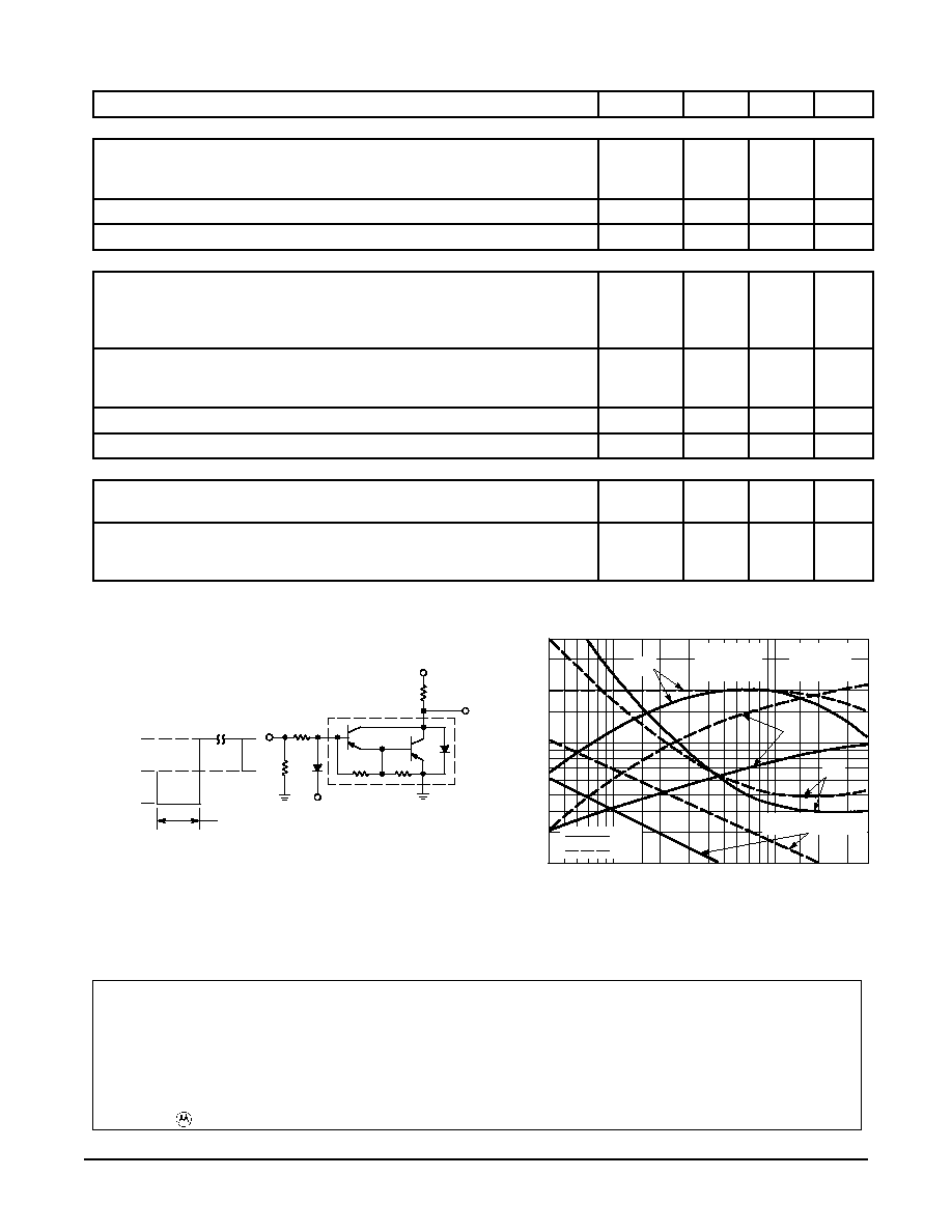
IC, COLLECTOR CURRENT (AMP)
VCC = 30 V
IC/IB = 250
t,
TIME (
s)
µ
2
1
0.8
0.6
0.4
0.2
ts
tf
Figure 1. Switching Times Test Circuit
Figure 2. Switching Times
V2
APPROX
+ 8 V
0
8 k
SCOPE
VCC
30 V
RC
51
FOR td AND tr, D1 IS DISCONNECTED
AND V2 = 0
FOR NPN TEST CIRCUIT REVERSE ALL POLARITIES.
25
µ
s
tr, tf
10 ns
DUTY CYCLE = 1%
+ 4 V
tr
td @ VBE(off) = 0 V
PNP
NPN
RB & RC VARIED TO OBTAIN DESIRED CURRENT LEVELS
D1, MUST BE FAST RECOVERY TYPE, e.g.:
1N5825 USED ABOVE IB
100 mA
MSD6100 USED BELOW IB
100 mA
V1
APPROX
12 V
TUT
RB
D1
60
0.4
2
IB1 = IB2
TJ = 25
°
C
Motorola reserves the right to make changes without further notice to any products herein. Motorola makes no warranty, representation or guarantee regarding
the suitability of its products for any particular purpose, nor does Motorola assume any liability arising out of the application or use of any product or circuit,
and specifically disclaims any and all liability, including without limitation consequential or incidental damages. "Typical" parameters can and do vary in different
applications. All operating parameters, including "Typicals" must be validated for each customer application by customer's technical experts. Motorola does
not convey any license under its patent rights nor the rights of others. Motorola products are not designed, intended, or authorized for use as components in
systems intended for surgical implant into the body, or other applications intended to support or sustain life, or for any other application in which the failure of
the Motorola product could create a situation where personal injury or death may occur. Should Buyer purchase or use Motorola products for any such
unintended or unauthorized application, Buyer shall indemnify and hold Motorola and its officers, employees, subsidiaries, affiliates, and distributors harmless
against all claims, costs, damages, and expenses, and reasonable attorney fees arising out of, directly or indirectly, any claim of personal injury or death
associated with such unintended or unauthorized use, even if such claim alleges that Motorola was negligent regarding the design or manufacture of the part.
Motorola and
are registered trademarks of Motorola, Inc. Motorola, Inc. is an Equal Opportunity/Affirmative Action Employer.
MJD112 MJD117
3
Motorola Bipolar Power Transistor Device Data
Figure 3. Thermal Response
t, TIME OR PULSE WIDTH (ms)
1
0.01
1000
0.3
0.2
0.07
r(t)
, EFFECTIVE
TRANSIENT
R
JC(t) = r(t) R
JC
R
JC = 6.25
°
C/W
D CURVES APPLY FOR POWER
PULSE TRAIN SHOWN
READ TIME AT t1
TJ(pk) TC = P(pk)
JC(t)
P(pk)
t1
t2
DUTY CYCLE, D = t1/t2
0.01
THERMAL
RESIST
ANCE (NORMALIZED)
0.7
0.5
0.1
0.05
0.03
0.02
0.02 0.03
0.05
0.1
0.2 0.3
0.5
1
2
3
5
10
20
30
50
100
200 300
500
0.2
SINGLE PULSE
D = 0.5
0.05
0.1
0.01
I C
, COLLECT
OR CURRENT
(AMP)
Figure 4. Maximum Rated Forward Biased
Safe Operating Area
Figure 5. Power Derating
2
VCE, COLLECTOREMITTER VOLTAGE (VOLTS)
0.3
100
5
2
0.5
0.2
BONDING WIRE LIMITED
THERMAL LIMIT
SECOND BREAKDOWN LIMIT
5
20
3
TJ = 150
°
C
CURVES APPLY BELOW RATED VCEO
100
µ
s
1 ms
dc
0.1
1
3
7
10
10
7
30
25
25
T, TEMPERATURE (
°
C)
0
50
75
100
125
150
20
15
10
5
P
D
, POWER DISSIP
A
TION (W
A
TTS)
2.5
0
2
1.5
1
0.5
TA TC
TA
SURFACE
MOUNT
TC
0.7
5 ms
50
70
200
500
µ
s
ACTIVEREGION SAFEOPERATING AREA
There are two limitations on the power handling ability of a
transistor: average junction temperature and second break-
down. Safe operating area curves indicate IC VCE limits of
the transistor that must be observed for reliable operation;
i.e., the transistor must not be subjected to greater dissipa-
tion than the curves indicate.
The data of Figures 5 and 6 is based on TJ(pk) = 150
_
C; TC
is variable depending on conditions. Second breakdown
pulse limits are valid for duty cycles to 10% provided TJ(pk)
< 150
_
C. TJ(pk) may be calculated from the data in Figure 4.
At high case temperatures, thermal limitations will reduce the
power that can be handled to values less than the limitations
imposed by second breakdown.
C, CAP
ACIT
ANCE (pF)
VR, REVERSE VOLTAGE (VOLTS)
Cib
0.04
30
1
4
10
40
TC = 25
°
C
200
10
50
70
100
0.1
2
6
20
20
PNP
NPN
0.6
0.4
0.2
0.06
Figure 6. Capacitance
Cob
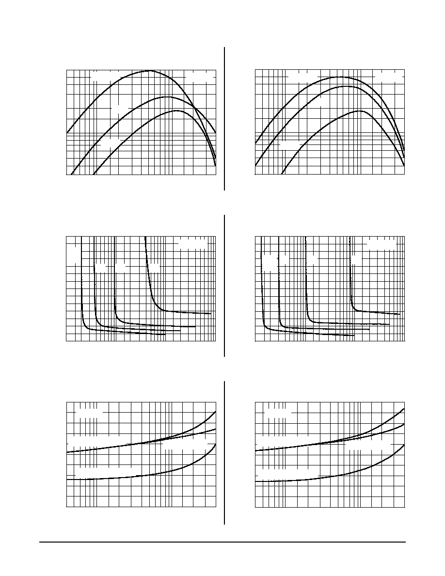
MJD112 MJD117
4
Motorola Bipolar Power Transistor Device Data
V
CE
, COLLECT
OREMITTER VOL
T
AGE (VOL
TS)
V
CE
, COLLECT
OREMITTER VOL
T
AGE (VOL
TS)
IC, COLLECTOR CURRENT (AMP)
NPN MJD112
PNP MJD117
Figure 7. DC Current Gain
Figure 8. Collector Saturation Region
Figure 9. "On Voltages
0.04
IC, COLLECTOR CURRENT (AMP)
300
0.06
0.2
2 k
800
4 k
h
FE
, DC CURRENT
GAIN
VCE = 3 V
TJ = 125
°
C
3 k
0.1
0.6
25
°
C
55
°
C
1 k
0.4
1
6 k
400
600
2
4
0.04
300
0.06
0.2
2 k
800
4 k
h
FE
, DC CURRENT
GAIN
3 k
0.1
0.6
25
°
C
55
°
C
1 k
0.4
1
6 k
400
600
2
4
3.4
IB, BASE CURRENT (mA)
2.6
2.2
1.8
1.4
0.6
0.1
0.2
0.5
10
2
5
IC =
0.5 A
1 A
1
3
1
0.04
IC, COLLECTOR CURRENT (AMP)
1.4
1
V
, VOL
T
AGE (VOL
TS)
2.2
1.8
0.6
0.2
TJ = 25
°
C
VBE(sat) @ IC/IB = 250
VBE @ VCE = 3 V
VCE(sat) @ IC/IB = 250
0.06
0.2
2
0.1
0.6
0.4
1
4
0.04
IC, COLLECTOR CURRENT (AMP)
1.4
1
V
, VOL
T
AGE (VOL
TS)
2.2
1.8
0.6
0.2
TJ = 25
°
C
VBE(sat) @ IC/IB = 250
VCE(sat) @ IC/IB = 250
0.06
0.2
2
0.1
0.6
0.4
1
4
20
50
100
3.4
IB, BASE CURRENT (mA)
2.6
2.2
1.8
1.4
0.6
0.1
0.2
0.5
10
2
5
1
3
1
20
50
100
VBE @ VCE = 3 V
TC = 125
°
C
VCE = 3 V
4 A
TJ = 125
°
C
2 A
TJ = 125
°
C
IC =
0.5 A
1 A
4 A
2 A
TYPICAL ELECTRICAL CHARACTERISTICS
MJD112 MJD117
5
Motorola Bipolar Power Transistor Device Data
NPN MJD112
PNP MJD117
0.04
IC, COLLECTOR CURRENT (AMP)
0.06
0.2
0
*APPLIED FOR IC/IB < hFE/3
0.1
0.6
55
°
C TO 25
°
C
0.4
1
4.8
2
4
104
VBE, BASEEMITTER VOLTAGE (VOLTS)
101
0
0.4
, COLLECT
OR CURRENT
(
A)
µ
I C
103
102
101
100
+ 0.2 + 0.4 + 0.6
TJ = 150
°
C
100
°
C
REVERSE
FORWARD
25
°
C
VCE = 30 V
105
0.6
0.2
+ 0.8
+ 1
+ 1.2 + 1.4
104
VBE, BASEEMITTER VOLTAGE (VOLTS)
101
0
+ 0.4
, COLLECT
OR CURRENT
(
A)
µ
I C
103
102
101
100
0.2 0.4 0.6
105
+ 0.6
+ 0.2
0.8
1
1.2 1.4
+ 0.8
4
3.2
2.4
1.6
0.8
VC FOR VBE
25
°
C TO 150
°
C
25
°
C TO 150
°
C
*
VC FOR VCE(sat)
0.04
IC, COLLECTOR CURRENT (AMP)
0.06
0.2
0.1
0.6
0.4
1
2
4
Figure 10. Temperature Coefficients
Figure 11. Collector CutOff Region
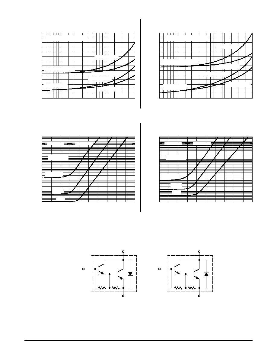
Figure 12. Darlington Schematic
BASE
EMITTER
COLLECTOR
8 k
120
PNP
BASE
EMITTER
COLLECTOR
8 k
120
NPN
0
4.8
+ 0.8
4
3.2
2.4
1.6
0.8
V
,
TEMPERA
TURE COEFFICIENTS (mV/
C)
°
V
,
TEMPERA
TURE COEFFICIENTS (mV/
C)
°
55
°
C TO 25
°
C
*APPLIES FOR IC/IB < hFE/3
*
VC FOR VCE(sat)
VB FOR VBE
25
°
C TO 150
°
C
55
°
C TO 25
°
C
25
°
C TO 150
°
C
55
°
C TO 25
°
C
VCE = 30 V
REVERSE
FORWARD
TJ = 150
°
C
100
°
C
25
°
C