 | ÐлекÑÑоннÑй компоненÑ: MMDF1N05E | СкаÑаÑÑ:  PDF PDF  ZIP ZIP |
Äîêóìåíòàöèÿ è îïèñàíèÿ www.docs.chipfind.ru
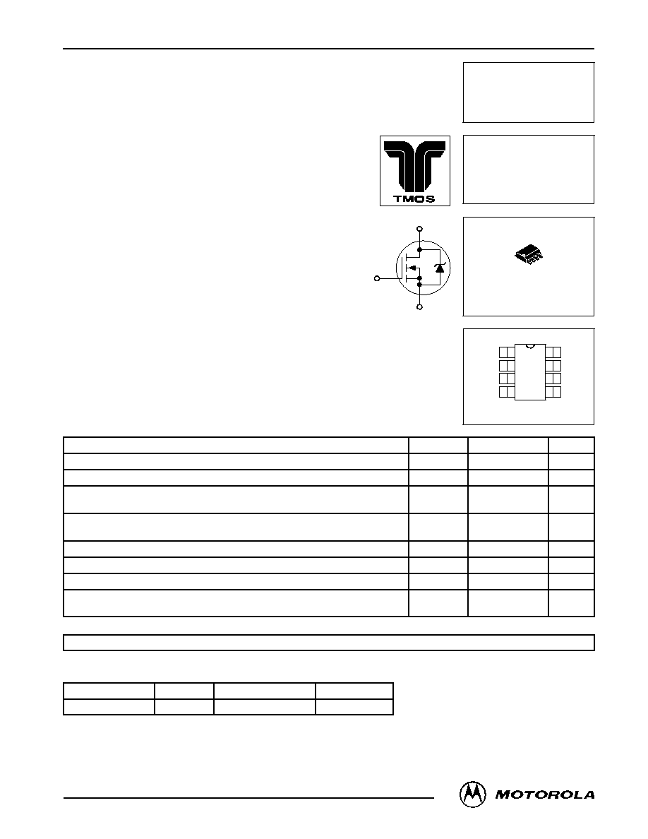
MMDF1N05E
DUAL TMOS MOSFET
50 VOLTS
1.5 AMPERE
RDS(on) = 0.30 OHM
®
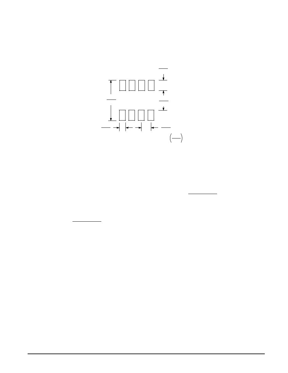
D
S
G
Source1
1
2
3
4
8
7
6
5
Top View
Gate1
Source2
Gate2
Drain1
Drain1
Drain2
Drain2
CASE 75105, Style 11
SO8
1
Motorola TMOS Power MOSFET Transistor Device Data
Medium Power Surface Mount Products
TMOS Dual N-Channel
Field Effect Transistors
MiniMOS
TM
devices are an advanced series of power MOSFETs
which utilize Motorola's TMOS process. These miniature surface
mount MOSFETs feature ultra low RDS(on) and true logic level
performance. They are capable of withstanding high energy in the
avalanche and commutation modes and the draintosource diode
has a low reverse recovery time. MiniMOS devices are designed
for use in low voltage, high speed switching applications where
power efficiency is important. Typical applications are dcdc
converters, and power management in portable and battery
powered products such as computers, printers, cellular and
cordless phones. They can also be used for low voltage motor
controls in mass storage products such as disk drives and tape
drives. The avalanche energy is specified to eliminate the
guesswork in designs where inductive loads are switched and offer
additional safety margin against unexpected voltage transients.
·
Ultra Low RDS(on) Provides Higher Efficiency and Extends Battery Life
·
Logic Level Gate Drive -- Can Be Driven by Logic ICs
·
Miniature SO8 Surface Mount Package -- Saves Board Space
·
Diode Is Characterized for Use In Bridge Circuits
·
Diode Exhibits High Speed
·
Avalanche Energy Specified
·
Mounting Information for SO8 Package Provided
·
IDSS Specified at Elevated Temperature
MAXIMUM RATINGS
(TJ = 25
°
C unless otherwise noted)
Rating
Symbol
Value
Unit
DraintoSource Voltage
VDS
50
Volts
GatetoSource Voltage -- Continuous
VGS
±
20
Volts
Drain Current -- Continuous
Drain Current
-- Pulsed
ID
IDM
2.0
10
Amps
Single Pulse DraintoSource Avalanche Energy -- Starting TJ = 25
°
C
(VDD = 25 V, VGS = 10 V, IL = 2 Apk)
EAS
300
mJ
Operating and Storage Temperature Range
TJ, Tstg
55 to 150
°
C
Total Power Dissipation @ TA = 25
°
C
PD
2.0
Watts
Thermal Resistance Junction to Ambient (1)
R
JA
62.5
°
C/W
Maximum Temperature for Soldering,
Time in Solder Bath
TL
260
10
°
C
Sec
DEVICE MARKING
F1N05
(1) Mounted on 2" square FR4 board (1" sq. 2 oz. Cu 0.06" thick single sided) with one die operating, 10 sec. max.
ORDERING INFORMATION
Device
Reel Size
Tape Width
Quantity
MMDF1N05ER2
13
12 mm embossed tape
2500
MiniMOS is a trademark of Motorola, Inc. TMOS is a registered trademark of Motorola, Inc.
Thermal Clad is a trademark of the Bergquist Company
REV 5
Order this document
by MMDF1N05E/D
MOTOROLA
SEMICONDUCTOR TECHNICAL DATA
©
Motorola, Inc. 1996
MMDF1N05E
2
Motorola TMOS Power MOSFET Transistor Device Data
ELECTRICAL CHARACTERISTICS
(TA = 25
°
C unless otherwise noted)
Characteristic
Symbol
Min
Typ
Max
Unit
OFF CHARACTERISTICS
DraintoSource Breakdown Voltage
(VGS = 0, ID = 250
µ
A)
V(BR)DSS
50
--
--
Vdc
Zero Gate Voltage Drain Current
(VDS = 50 V, VGS = 0)
IDSS
--
--
250
µ
Adc
GateBody Leakage Current
(VGS = 20 Vdc, VDS = 0)
IGSS
--
--
100
nAdc
ON CHARACTERISTICS(1)
Gate Threshold Voltage
(VDS = VGS, ID = 250
µ
Adc)
VGS(th)
1.0
--
3.0
Vdc
DraintoSource OnResistance
(VGS = 10 Vdc, ID = 1.5 Adc)
(VGS = 4.5 Vdc, ID = 0.6 Adc)
RDS(on)
RDS(on)
--
--
--
--
0.30
0.50
Ohms
Forward Transconductance (VDS = 15 V, ID = 1.5 A)
gFS
--
1.5
--
mhos
DYNAMIC CHARACTERISTICS
Input Capacitance
(VDS = 25 V, VGS = 0,
f = 1.0 MHz)
Ciss
--
330
--
pF
Output Capacitance
(VDS = 25 V, VGS = 0,
f = 1.0 MHz)
Coss
--
160
--
Reverse Transfer Capacitance
f = 1.0 MHz)
Crss
--
50
--
SWITCHING CHARACTERISTICS(2)
TurnOn Delay Time
(VDD = 10 V, ID = 1.5 A, RL = 10
,
VG = 10 V, RG = 50
)
td(on)
--
--
20
ns
Rise Time
(VDD = 10 V, ID = 1.5 A, RL = 10
,
VG = 10 V, RG = 50
)
tr
--
--
30
TurnOff Delay Time
(VDD = 10 V, ID = 1.5 A, RL = 10
,
VG = 10 V, RG = 50
)
td(off)
--
--
40
Fall Time
tf
--
--
25
Total Gate Charge
(VDS = 10 V, ID = 1.5 A,
VGS = 10 V)
Qg
--
12.5
--
nC
GateSource Charge
(VDS = 10 V, ID = 1.5 A,
VGS = 10 V)
Qgs
--
1.9
--
GateDrain Charge
VGS = 10 V)
Qgd
--
3.0
--
SOURCEDRAIN DIODE CHARACTERISTICS (TC = 25
°
C)
Forward Voltage(1)
(IS = 1.5 A, VGS = 0 V)
(dIS/dt = 100 A/
µ
s)
VSD
--
--
1.6
V
Reverse Recovery Time
(IS = 1.5 A, VGS = 0 V)
(dIS/dt = 100 A/
µ
s)
trr
--
45
--
ns
(1) Pulse Test: Pulse Width
300
µ
s, Duty Cycle
2.0%.
(2) Switching characteristics are independent of operating junction temperature.
MMDF1N05E
3
Motorola TMOS Power MOSFET Transistor Device Data
0.1
0
0
7
0
2
4
6
10
8
6
4
2
I D
, DRAIN CURRENT
(AMPS)
10
8
6
4
2
0
0
2
4
6
8
10
VDS, DRAINTOSOURCE VOLTAGE (VOLTS)
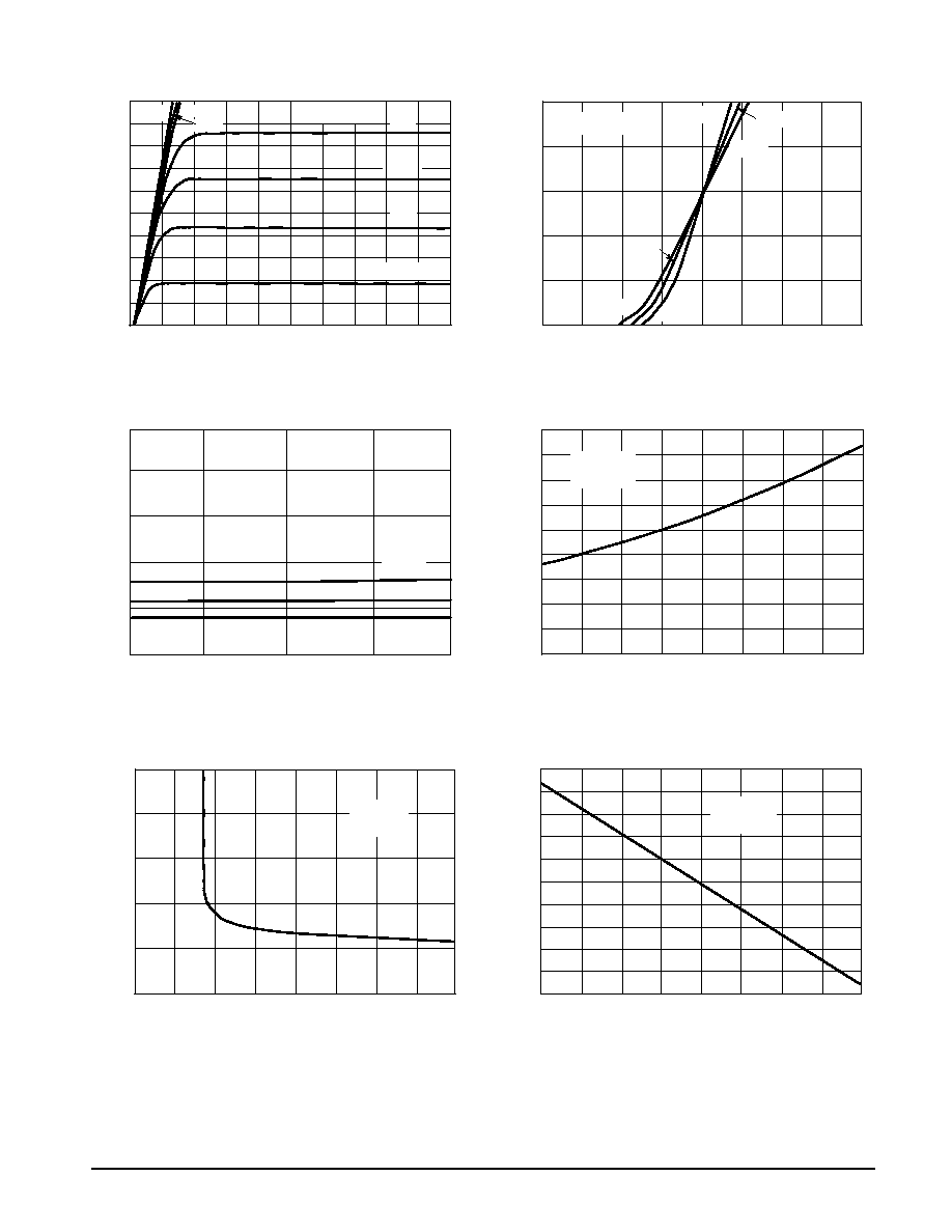
TYPICAL ELECTRICAL CHARACTERISTICS
Figure 1. OnRegion Characteristics
Figure 2. Transfer Characteristics
Figure 3. OnResistance versus Drain Current
Figure 4. OnResistance Variation with Temperature
I D
, DRAIN CURRENT
(AMPS)
VGS, GATETOSOURCE VOLTAGE (VOLTS)
R
DS(on)
, DRAINT
OSOURCE ONRESIST
ANCE (OHMS)
0
2
4
6
8
ID, DRAIN CURRENT (AMPS)
TJ, JUNCTION TEMPERATURE (
°
C)
50
0
50
100
150
1.8
1.6
1.2
0.8
0.4
0
R
DS(on)
, DRAINT
OSOURCE ONRESIST
ANCE
(NORMALIZED)
VGS = 10 V
0.2
0.3
0.4
0.5
100
°
C
25
°
C
55
°
C
4 V
1
3
5
8
VGS = 10 V
ID = 1.5 A
TJ = 25
°
C
5 V
6 V
25
°
C
0.2
0.6
1
1.4
25
25
75
125
8 V
4.5 V
10 V
55
°
C
25
°
C
100
°
C
55
°
C
VGS = 3.5 V
VDS
10 V
100
°
C
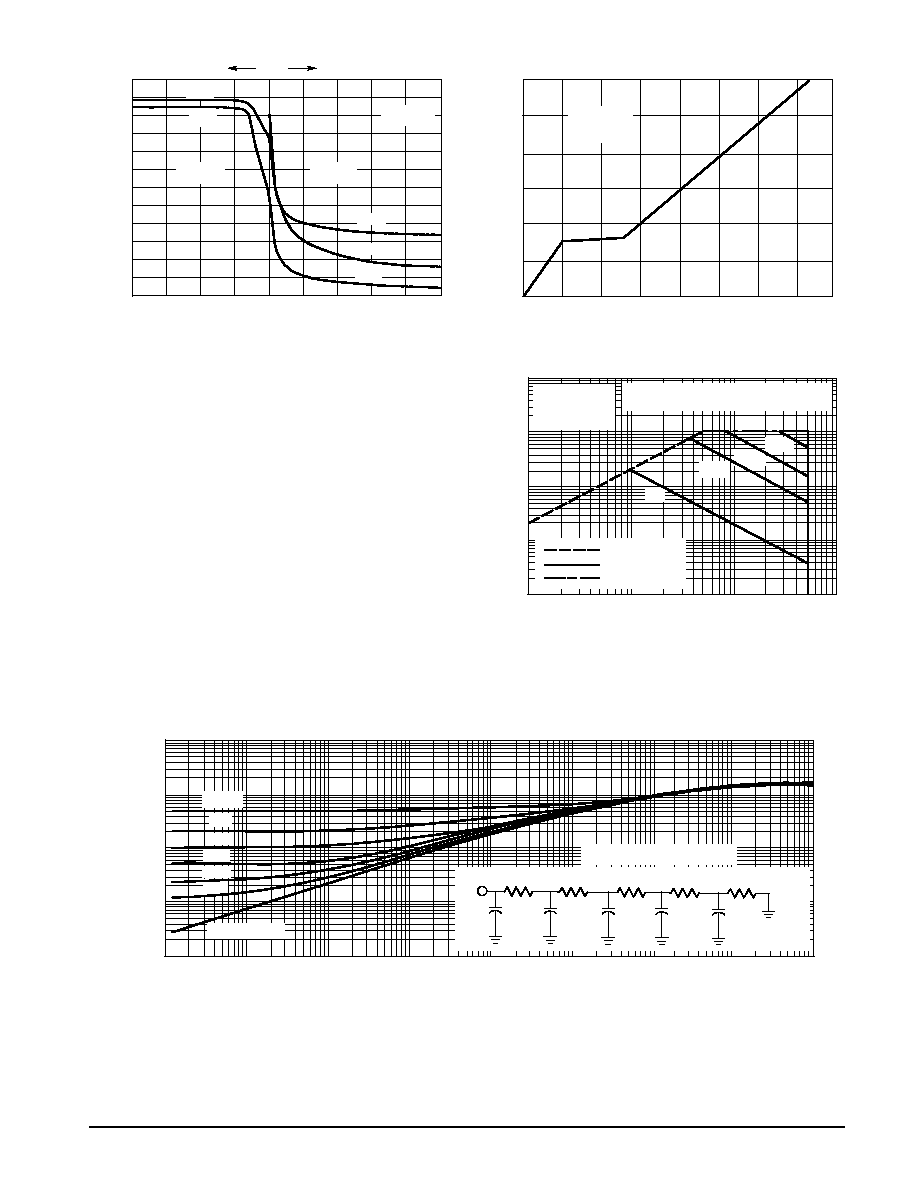
Figure 5. On Resistance versus
GateToSource Voltage
Figure 6. Gate Threshold Voltage Variation
with Temperature
150
125
100
75
50
25
0
25
50
1.2
1.1
1
0.9
0.8
0.7
V
GS(th)
, GA
TE
THRESHOLD VOL
T
AGE (NORMALIZED)
TJ, JUNCTION TEMPERATURE (
°
C)
VDS = VGS
ID = 1 mA
0.5
0.4
0.3
0.2
0
2
3
TJ, JUNCTION TEMPERATURE
ID = 1.5 A
VGS = 0
0.1
4
5
6
7
8
9
10
R
DS(on)
, DRAINT
OSOURCE RESIST
ANCE (OHMS)
MMDF1N05E
4
Motorola TMOS Power MOSFET Transistor Device Data
0
VGS
VDS
Ciss
Coss
16
10
6
0
12
10
8
6
4
2
0
Qg, TOTAL GATE CHARGE (nC)
V
GS
, GA
TET
OSOURCE VOL
T
AGE (VOL
TS)
Figure 7. Capacitance Variation
2
4
8
12
14
Figure 8. Gate Charge versus
GateToSource Voltage
1200
1000
800
600
400
0
20
10
0
20
C, CAP
ACIT
ANCE (pF)
GATETOSOURCE OR DRAINTOSOURCE VOLTAGE (VOLTS)
200
15
5
5
10
15
VDS = 25 V
ID = 1.2 A
VDS = 0
Ciss
Crss
Crss
VGS = 0
TJ = 25
°
C
25
SAFE OPERATING AREA INFORMATION
Forward Biased Safe Operating Area
The FBSOA curves define the maximum draintosource
voltage and drain current that a device can safely handle
when it is forward biased, or when it is on, or being turned on.
Because these curves include the limitations of simultaneous
high voltage and high current, up to the rating of the device,
they are especially useful to designers of linear systems. The
curves are based on a case temperature of 25
°
C and a maxi-
mum junction temperature of 150
°
C. Limitations for repetitive
pulses at various case temperatures can be determined by
using the thermal response curves. Motorola Application
Note, AN569, "Transient Thermal Resistance -- General
Data and Its Use" provides detailed instructions.
Figure 9. Maximum Rated Forward Biased
Safe Operating Area
0.1
VDS, DRAINTOSOURCE VOLTAGE (VOLTS)
1
10
I D
, DRAIN CURRENT
(AMPS)
RDS(on) LIMIT
THERMAL LIMIT
PACKAGE LIMIT
0.01
VGS = 20 V
SINGLE PULSE
TC = 25
°
C
10
0.1
dc
10 ms
1
100
100
Mounted on 2" sq. FR4 board (1" sq. 2 oz. Cu 0.06"
thick single sided) with one die operating, 10s max.
100
µ
s
10
µ
s
Figure 10. Thermal Response
t, TIME (s)
Rthja(t)
, EFFECTIVE
TRANSIENT
THERMAL
RESIST
ANCE
1
0.1
0.01
D = 0.5
SINGLE PULSE
1.0E05
1.0E04
1.0E03
1.0E02
1.0E01
1.0E+00
1.0E+01
0.2
0.1
0.05
0.02
0.01
1.0E+02
1.0E+03
0.001
10
0.0175
0.0710
0.2706
0.5776
0.7086
107.55 F
1.7891 F
0.3074 F
0.0854 F
0.0154 F
Chip
Ambient
Normalized to
ja at 10s.
MMDF1N05E
5
Motorola TMOS Power MOSFET Transistor Device Data
INFORMATION FOR USING THE SO8 SURFACE MOUNT PACKAGE
MINIMUM RECOMMENDED FOOTPRINT FOR SURFACE MOUNTED APPLICATIONS
Surface mount board layout is a critical portion of the total
design. The footprint for the semiconductor packages must be
the correct size to insure proper solder connection interface
between the board and the package. With the correct pad
geometry, the packages will selfalign when subjected to a
solder reflow process.
mm
inches
0.060
1.52
0.275
7.0
0.024
0.6
0.050
1.270
0.155
4.0
SO8 POWER DISSIPATION
The power dissipation of the SO8 is a function of the input
pad size. These can vary from the minimum pad size for
soldering to the pad size given for maximum power
dissipation. Power dissipation for a surface mount device is
determined by TJ(max), the maximum rated junction
temperature of the die, R
JA, the thermal resistance from the
device junction to ambient; and the operating temperature, TA.
Using the values provided on the data sheet for the SO8
package, PD can be calculated as follows:
PD =
TJ(max) TA
R
JA
The values for the equation are found in the maximum
ratings table on the data sheet. Substituting these values into
the equation for an ambient temperature TA of 25
°
C, one can
calculate the power dissipation of the device which in this case
is 2.0 Watts.
PD =
150
°
C 25
°
C
62.5
°
C/W
= 2.0 Watts
The 62.5
°
C/W for the SO8 package assumes the
recommended footprint on a glass epoxy printed circuit board
to achieve a power dissipation of 2.0 Watts using the footprint
shown. Another alternative would be to use a ceramic
substrate or an aluminum core board such as Thermal Clad
TM
.
Using board material such as Thermal Clad, the power
dissipation can be doubled using the same footprint.
SOLDERING PRECAUTIONS
The melting temperature of solder is higher than the rated
temperature of the device. When the entire device is heated
to a high temperature, failure to complete soldering within a
short time could result in device failure. Therefore, the
following items should always be observed in order to
minimize the thermal stress to which the devices are
subjected.
·
Always preheat the device.
·
The delta temperature between the preheat and soldering
should be 100
°
C or less.*
·
When preheating and soldering, the temperature of the
leads and the case must not exceed the maximum
temperature ratings as shown on the data sheet. When
using infrared heating with the reflow soldering method,
the difference shall be a maximum of 10
°
C.
·
The soldering temperature and time shall not exceed
260
°
C for more than 10 seconds.
·
When shifting from preheating to soldering, the maximum
temperature gradient shall be 5
°
C or less.
·
After soldering has been completed, the device should be
allowed to cool naturally for at least three minutes.
Gradual cooling should be used as the use of forced
cooling will increase the temperature gradient and result
in latent failure due to mechanical stress.
·
Mechanical stress or shock should not be applied during
cooling
* Soldering a device without preheating can cause excessive
thermal shock and stress which can result in damage to the
device.
MMDF1N05E
6
Motorola TMOS Power MOSFET Transistor Device Data
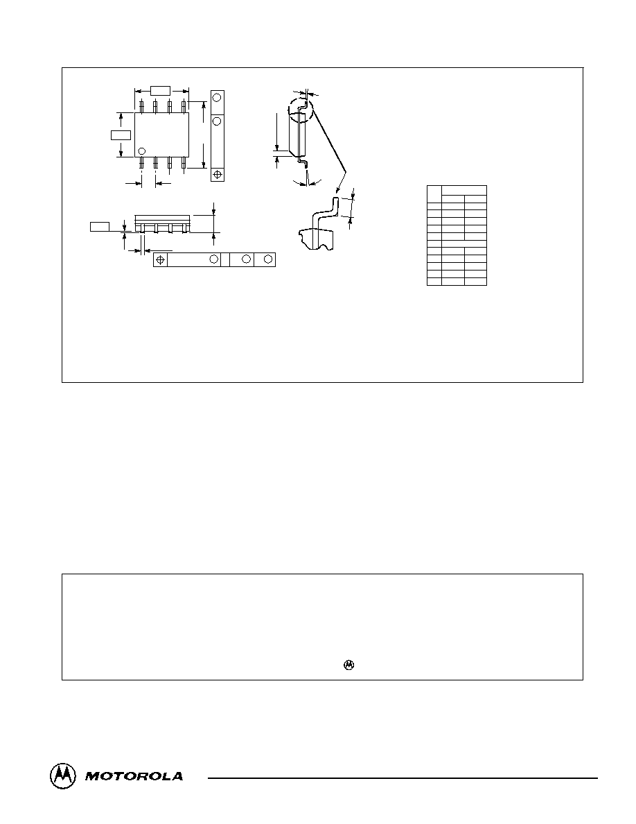
PACKAGE DIMENSIONS
STYLE 11:
PIN 1.
SOURCE 1
2.
GATE 1
3.
SOURCE 2
4.
GATE 2
5.
DRAIN 2
6.
DRAIN 2
7.
DRAIN 1
8.
DRAIN 1
CASE 75105
SO8
ISSUE P
SEATING
PLANE
1
4
5
8
C
K
4X
P
A
0.25 (0.010)
M
T B
S
S
0.25 (0.010)
M
B
M
8X
D
R
M
J
X 45
_
_
F
A
B
T
DIM
MIN
MAX
MILLIMETERS
A
4.80
5.00
B
3.80
4.00
C
1.35
1.75
D
0.35
0.49
F
0.40
1.25
G
1.27 BSC
J
0.18
0.25
K
0.10
0.25
M
0
7
P
5.80
6.20
R
0.25
0.50
_
_
G
NOTES:
1. DIMENSIONS A AND B ARE DATUMS AND T IS A
DATUM SURFACE.
2. DIMENSIONING AND TOLERANCING PER ANSI
Y14.5M, 1982.
3. DIMENSIONS ARE IN MILLIMETER.
4. DIMENSION A AND B DO NOT INCLUDE MOLD
PROTRUSION.
5. MAXIMUM MOLD PROTRUSION 0.15 PER SIDE.
6. DIMENSION D DOES NOT INCLUDE MOLD
PROTRUSION. ALLOWABLE DAMBAR
PROTRUSION SHALL BE 0.127 TOTAL IN EXCESS
OF THE D DIMENSION AT MAXIMUM MATERIAL
CONDITION.
Motorola reserves the right to make changes without further notice to any products herein. Motorola makes no warranty, representation or guarantee regarding
the suitability of its products for any particular purpose, nor does Motorola assume any liability arising out of the application or use of any product or circuit, and
specifically disclaims any and all liability, including without limitation consequential or incidental damages. "Typical" parameters which may be provided in Motorola
data sheets and/or specifications can and do vary in different applications and actual performance may vary over time. All operating parameters, including "Typicals"
must be validated for each customer application by customer's technical experts. Motorola does not convey any license under its patent rights nor the rights of
others. Motorola products are not designed, intended, or authorized for use as components in systems intended for surgical implant into the body, or other
applications intended to support or sustain life, or for any other application in which the failure of the Motorola product could create a situation where personal injury
or death may occur. Should Buyer purchase or use Motorola products for any such unintended or unauthorized application, Buyer shall indemnify and hold Motorola
and its officers, employees, subsidiaries, affiliates, and distributors harmless against all claims, costs, damages, and expenses, and reasonable attorney fees
arising out of, directly or indirectly, any claim of personal injury or death associated with such unintended or unauthorized use, even if such claim alleges that
Motorola was negligent regarding the design or manufacture of the part. Motorola and are registered trademarks of Motorola, Inc. Motorola, Inc. is an Equal
Opportunity/Affirmative Action Employer.
How to reach us:
USA / EUROPE / Locations Not Listed: Motorola Literature Distribution;
JAPAN: Nippon Motorola Ltd.; TatsumiSPDJLDC, 6F SeibuButsuryuCenter,
P.O. Box 20912; Phoenix, Arizona 85036. 18004412447 or 6023035454
3142 Tatsumi KotoKu, Tokyo 135, Japan. 038135218315
MFAX: RMFAX0@email.sps.mot.com TOUCHTONE 6022446609
ASIA/PACIFIC: Motorola Semiconductors H.K. Ltd.; 8B Tai Ping Industrial Park,
INTERNET: http://DesignNET.com
51 Ting Kok Road, Tai Po, N.T., Hong Kong. 85226629298
MMDF1N05E/D
*MMDF1N05E/D*