 | –≠–ª–µ–∫—Ç—Ä–æ–Ω–Ω—ã–π –∫–æ–º–ø–æ–Ω–µ–Ω—Ç: MPC952 | –°–∫–∞—á–∞—Ç—å:  PDF PDF  ZIP ZIP |

MOTOROLA
SEMICONDUCTOR TECHNICAL DATA
1
REV 3
©
Motorola, Inc. 1998
2/98
Low Voltage PLL Clock Driver
The MPC952 is a 3.3V compatible, PLL based clock driver device
targeted for high performance clock tree applications. The device
features a fully integrated PLL with no external components required.
With output frequencies of up to 180MHz and eleven low skew outputs
the MPC952 is well suited for high performance designs. The device
employs a fully differential PLL design to optimize jitter and noise
rejection performance. Jitter is an increasingly important parameter as
more microprocessors and ASiC's are employing on chip PLL clock
distribution.
∑
Fully Integrated PLL
∑
Output Frequency up to 180MHz
∑
High Impedance Disabled Outputs
∑
Compatible with PowerPC
TM
, Intel and High Performance RISC
Microprocessors
∑
Output Frequency Configurable
∑
TQFP Packaging
∑
±
100ps Cycle≠to≠Cycle Jitter
The MPC952 features three banks of individually configurable outputs.
The banks contain 5 outputs, 4 outputs and 2 outputs. The internal divide
circuitry allows for output frequency ratios of 1:1, 2:1, 3:1 and 3:2:1. The
output frequency relationship is controlled by the fsel frequency control
pins. The fsel pins as well as the other inputs are LVCMOS/LVTTL
compatible inputs.
The MPC952 uses external feedback to the PLL. This features allows
for the use of the device as a "zero delay" buffer. Any of the eleven
outputs can be used as the feedback to the PLL. The VCO_Sel pin allows for the choice of two VCO ranges to optimize PLL
stability and jitter performance. The MR/OE pin allows the user to force the outputs into high impedance for board level test.
For system debug the PLL of the MPC952 can be bypassed. When forced to a logic HIGH, the PLLEN input will route the
signal on the RefClk input around the PLL directly to the internal dividers. Because the signal is routed through the dividers, it
may take several transitions of the RefClk to affect a transition on the outputs. This features allows a designer to single step the
design for debug purposes.
The outputs of the MPC952 are LVCMOS outputs. The outputs are optimally designed to drive terminated transmission lines.
For applications using series terminated transmission lines each MPC952 output can drive two lines. This capability provides an
effective fanout of 22, more than enough clocks for most clock tree designs. For more information on driving transmission lines
consult the applications section of this data sheet.
PowerPC is a trademark of International Business Machines Corporation. Pentium is a trademark of Intel Corporation.
MPC952
LOW VOLTAGE
PLL CLOCK DRIVER
FA SUFFIX
TQFP PACKAGE
CASE 873A-02
MPC952
MOTOROLA
ECLinPS and ECLinPS Lite
DL140 -- Rev 3
2
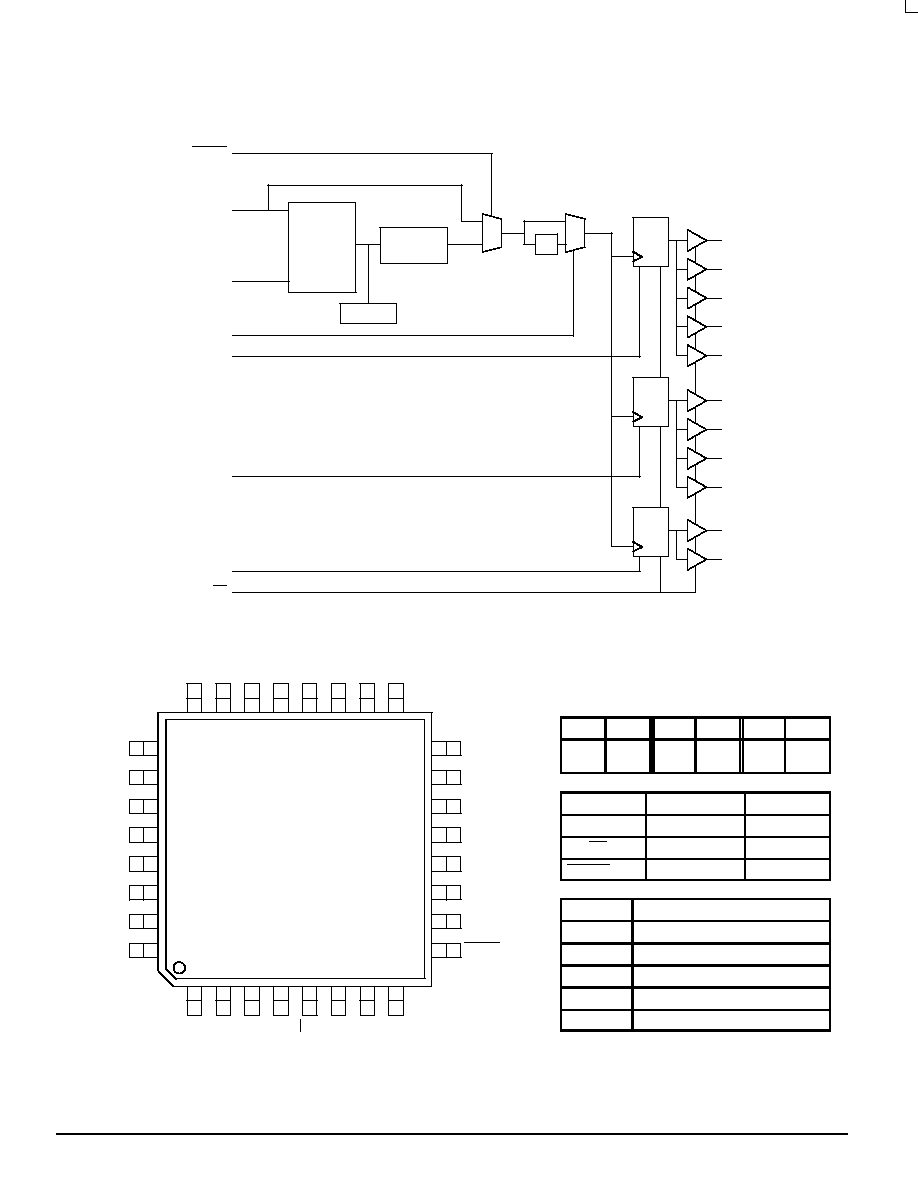
Figure 1. MPC952 Logic Diagram
VCO
200≠480MHz
PHASE
DETECTOR
LPF
fsela
VCO_Sel
FBin
˜
4/
˜
6
Qa0
Qa1
Qa2
Qa3
Qa4
REFCLK
PLL_En
˜
2
fselb
˜
4/
˜
2
Qb0
Qb1
Qb2
Qb3
fselc
˜
2/
˜
4
Qc0
Qc1
MR/OE
(Int Pull Down)
(Int Pull Down)
(Int Pull Down)
(Int Pull Down)
(Int Pull Down)
FUNCTION TABLES
fsela
Qan
fselb
Qbn
fselc
Qcn
0
1
˜
4
˜
6
0
1
˜
4
˜
2
0
1
˜
2
˜
4
Control Pin
Logic `0'
Logic `1'
VCO_Sel
fVCO
fVCO/2
MR/OE
Output Enable
High Z
PLL_En
Enable PLL
Disable PLL
Pin Name
Description
VCCA
PLL Power Supply
VCCO
Output Buffer Power Supply
VCCI
Internal Core Logic Power Supply
GNDI
Internal Ground
GNDO
Output Buffer Ground
PLL_En
VCCO
Qb2
Qb3
GNDO
GNDO
Qc0
Qc1
VCCO
VCCO
Qa2
Qa1
GNDO
Qa0
VCCI
VCCA
GNDO
Qb1
Qb0
VCCO
VCCO
Qa4
Qa3
GNDO
VCO_Sel
fselc
fselb
fsela
MR/OE
REFCLK
GNDI
FBin
25
26
27
28
29
30
31
32
15
14
13
12
11
10
9
1
2
3
4
5
6
7
8
24
23
22
21
20
19
18
17
16
MPC952
Figure 2. 32≠Lead Pinout (Top View)

MPC952
ECLinPS and ECLinPS Lite
DL140 -- Rev 3
3
MOTOROLA
ABSOLUTE MAXIMUM RATINGS*
Symbol
Parameter
Min
Max
Unit
VCC
Supply Voltage
≠0.3
4.6
V
VI
Input Voltage
≠0.3
VDD + 0.3
V
IIN
Input Current
±
20
mA
TStor
Storage Temperature Range
≠40
125
∞
C
* Absolute maximum continuous ratings are those values beyond which damage to the device may occur. Exposure to these conditions or
conditions beyond those indicated may adversely affect device reliability. Functional operation under absolute-maximum-rated conditions is not
implied.
DC CHARACTERISTICS (TA = 0
∞
to 70
∞
C, VCC = 3.3V
±
5%)
Symbol
Characteristic
Min
Typ
Max
Unit
Condition
VIH
Input HIGH Voltage
2.0
3.6
V
VIL
Input LOW Voltage
0.8
V
VOH
Output HIGH Voltage
2.4
V
IOH = ≠20mA (Note 1.)
VOL
Output LOW Voltage
0.5
V
IOL = 20mA (Note 1.)
IIN
Input Current
±
120
µ
A
Note 2.
CIN
Input Capacitance
2.7
4
pF
Cpd
Power Dissipation Capacitance
25
pF
ICC
Maximum Quiescent Supply Current
160
mA
Total ICC Static Current
ICCA
PLL Supply Current
15
20
mA
1. The MPC952 outputs can drive series or parallel terminated 50
(or 50
to VCC/2) transmission lines on the incident edge (see Applications
Info section).
2. Inputs have pull≠up, pull≠down resistors which affect input current.
PLL INPUT REFERENCE CHARACTERISTICS (TA = 0 to 70
∞
C)
Symbol
Characteristic
Min
Max
Unit
Condition
tr, tf
TCLK Input Rise/Falls
3.0
ns
fref
Reference Input Frequency
Note 3.
Note 3.
MHz
frefDC
Reference Input Duty Cycle
25
75
%
3. Maximum and minimum input reference is limited by the VCO lock range and the feedback divider.

MPC952
MOTOROLA
ECLinPS and ECLinPS Lite
DL140 -- Rev 3
4
AC CHARACTERISTICS (TA = 0
∞
to 70
∞
C, VCC = 3.3V
±
5%)
Symbol
Characteristic
Min
Typ
Max
Unit
Condition
tr, tf
Output Rise/Fall Time (Note 4.)
0.10
1.0
ns
0.8 to 2.0V
tpw
Output Pulse Width (Note 4.)
tCYCLE/2
≠750
tCYCLE/2
±
500
tCYCLE/2
+750
ps
tos
Output-to-Output Skew
Excluding Qa0
(Note 4.)
All Outputs
All Outputs
350
450
550
ps
Same Frequencies
Same Frequencies
Different Frequencies
fVCO
PLL VCO Lock Range
Feedback = VCO/4
Feedback = VCO/6
Feedback = VCO/8
Feedback = VCO/12
200
200
200
200
480
480
480
480
MHz
VCO_Sel = 0
VCO_Sel = 0
VCO_Sel = 1
VCO_Sel = 1
fmax
Maximum Output Frequency
Qc,Qb (
˜
2)
Qa,Qb,Qc (
˜
4)
Qa (
˜
6)
180
120
80
MHz
(Note 4.)
tpd
REFCLK to FBIN Delay
≠200
0
200
ps
Notes 4., 5.
tPLZ, tPHZ
Output Disable Time
2
8
ns
50
to VCC/2
tPZL, tPLH
Output Enable Time
2
10
ns
50
to VCC/2
tjitter
Cycle≠to≠Cycle Jitter (Peak≠to≠Peak)
±
100
ps
tlock
Maximum PLL Lock Time
10
ms
4. 50
to VCC/2.
5. tpd is specified for 50MHz input ref, the window will shrink/grow proportionally from the minimum limit with shorter/longer input reference periods.
The tpd does not include jitter.
APPLICATIONS INFORMATION
Driving Transmission Lines
The MPC952 clock driver was designed to drive high
speed signals in a terminated transmission line environment.
To provide the optimum flexibility to the user the output
drivers were designed to exhibit the lowest impedance
possible. With an output impedance of less than 10
the
drivers can drive either parallel or series terminated
transmission lines. For more information on transmission
lines the reader is referred to application note AN1091 in the
Timing Solutions brochure (BR1333/D).
Figure 3. Single versus Dual Transmission Lines
7
IN
MPC952
OUTPUT
BUFFER
RS = 43
ZO = 50
OutA
7
IN
MPC952
OUTPUT
BUFFER
RS = 43
ZO = 50
OutB0
RS = 43
ZO = 50
OutB1
In most high performance clock networks point≠to≠point
distribution of signals is the method of choice. In a
point≠to≠point scheme either series terminated or parallel
terminated transmission lines can be used. The parallel
technique terminates the signal at the end of the line with a
50
resistance to VCC/2. This technique draws a fairly high
level of DC current and thus only a single terminated line can
be driven by each output of the MPC952 clock driver. For the
series terminated case however there is no DC current draw,
thus the outputs can drive multiple series terminated lines.
Figure 3 illustrates an output driving a single series
terminated line vs two series terminated lines in parallel.
When taken to its extreme the fanout of the MPC952 clock
driver is effectively doubled due to its capability to drive
multiple lines.
The waveform plots of Figure 4 show the simulation
results of an output driving a single line vs two lines. In both
cases the drive capability of the MPC952 output buffers is
more than sufficient to drive 50
transmission lines on the
incident edge. Note from the delay measurements in the
simulations a delta of only 43ps exists between the two
differently loaded outputs. This suggests that the dual line
driving need not be used exclusively to maintain the tight
output≠to≠output skew of the MPC952. The output waveform
in Figure 4 shows a step in the waveform, this step is caused
by the impedance mismatch seen looking into the driver. The
parallel combination of the 43
series resistor plus the output
impedance does not match the parallel combination of the
line impedances. The voltage wave launched down the two
lines will equal:

MPC952
ECLinPS and ECLinPS Lite
DL140 -- Rev 3
5
MOTOROLA
VL = VS (Zo / Rs + Ro +Zo) = 3.0 (25/53.5) = 1.40V
At the load end the voltage will double, due to the near
unity reflection coefficient, to 2.8V. It will then increment
towards the quiescent 3.0V in steps separated by one round
trip delay (in this case 4.0ns).
Figure 4. Single versus Dual Waveforms
TIME (nS)
VOL
T
AGE (V)
3.0
2.5
2.0
1.5
1.0
0.5
0
2
4
6
8
10
12
14
OutB
tD = 3.9386
OutA
tD = 3.8956
In
Since this step is well above the threshold region it will not
cause any false clock triggering, however designers may be
uncomfortable with unwanted reflections on the line. To
better match the impedances when driving multiple lines the
situation in Figure 5 should be used. In this case the series
terminating resistors are reduced such that when the parallel
combination is added to the output buffer impedance the line
impedance is perfectly matched.
Figure 5. Optimized Dual Line Termination
7
MPC952
OUTPUT
BUFFER
RS = 36
ZO = 50
RS = 36
ZO = 50
7
+ 36
k
36
= 50
k
50
25
= 25
SPICE level output buffer models are available for
engineers who want to simulate their specific interconnect
schemes. In addition IV characteristics are in the process of
being generated to support the other board level simulators in
general use.
Power Supply Filtering
The MPC952 is a mixed analog/digital product and as
such it exhibits some sensitivities that would not necessarily
be seen on a fully digital product. Analog circuitry is naturally
susceptible to random noise, especially if this noise is seen
on the power supply pins. The MPC952 provides separate
power supplies for the output buffers (VCCO) and the internal
PLL (VCCA) of the device. The purpose of this design
technique is to try and isolate the high switching noise digital
outputs from the relatively sensitive internal analog
phase≠locked loop. In a controlled environment such as an
evaluation board this level of isolation is sufficient. However,
in a digital system environment where it is more difficult to
minimize noise on the power supplies a second level of
isolation may be required. The simplest form of isolation is a
power supply filter on the VCCA pin for the MPC952.
Figure 6. Power Supply Filter
VCCA
VCC
MPC952
0.01
µ
F
22
µ
F
0.01
µ
F
3.3V
RS=5≠15
Figure 6 illustrates a typical power supply filter scheme.
The MPC952 is most susceptible to noise with spectral
content in the 1KHz to 1MHz range. Therefore the filter
should be designed to target this range. The key parameter
that needs to be met in the final filter design is the DC voltage
drop that will be seen between the VCC supply and the VCCA
pin of the MPC952. From the data sheet the IVCCA current
(the current sourced through the VCCA pin) is typically 15mA
(20mA maximum), assuming that a minimum of 3.0V must be
maintained on the VCCA pin very little DC voltage drop can
be tolerated when a 3.3V VCC supply is used. The resistor
shown in Figure 6 must have a resistance of 10≠15
to meet
the voltage drop criteria. The RC filter pictured will provide a
broadband filter with approximately 100:1 attenuation for
noise whose spectral content is above 20KHz. As the noise
frequency crosses the series resonant point of an individual
capacitor it's overall impedance begins to look inductive and
thus increases with increasing frequency. The parallel
capacitor combination shown ensures that a low impedance
path to ground exists for frequencies well above the
bandwidth of the PLL.
Although the MPC952 has several design features to
minimize the susceptibility to power supply noise (isolated
power and grounds and fully differential PLL) there still may
be applications in which overall performance is being
degraded due to system power supply noise. The power
supply filter schemes discussed in this section should be
adequate to eliminate power supply noise related problems
in most designs.