 | –≠–ª–µ–∫—Ç—Ä–æ–Ω–Ω—ã–π –∫–æ–º–ø–æ–Ω–µ–Ω—Ç: MRF20030 | –°–∫–∞—á–∞—Ç—å:  PDF PDF  ZIP ZIP |
1
MRF20030
MOTOROLA RF DEVICE DATA
The RF Sub≠Micron Bipolar Line
RF Power Bipolar Transistor
Designed for broadband commercial and industrial applications at frequen-
cies from 1800 to 2000 MHz. The high gain and broadband performance of this
device makes it ideal for large≠signal, common≠emitter class A and class AB
amplifier applications. Suitable for frequency modulated, amplitude modulated
and multi≠carrier base station RF power amplifiers.
∑
Specified 26 Volts, 2.0 GHz, Class AB, Two≠Tones Characteristics
Output Power -- 30 Watts (PEP)
Power Gain -- 9.8 dB
Efficiency -- 34%
Intermodulation Distortion -- ≠28 dBc
∑
Typical 26 Volts, 1.88 GHz, Class AB, CW Characteristics
Output Power -- 30 Watts
Power Gain -- 10.5 dB
Efficiency -- 40%
∑
Excellent Thermal Stability
∑
Capable of Handling 3:1 VSWR @ 26 Vdc, 2000 MHz, 30 Watts (PEP)
Output Power
∑
Characterized with Series Equivalent Large≠Signal Impedance Parameters
∑
S≠Parameter Characterization at High Bias Levels
∑
Designed for FM, TDMA, CDMA, and Multi≠Carrier Applications
MAXIMUM RATINGS
Rating
Symbol
Value
Unit
Collector≠Emitter Voltage
VCEO
25
Vdc
Collector≠Emitter Voltage
VCES
60
Vdc
Collector≠Base Voltage
VCBO
60
Vdc
Collector≠Emitter Voltage (RBE = 100
)
VCER
30
Vdc
Emitter≠Base Voltage
VEB
≠3
Vdc
Collector Current ≠ Continuous
IC
4
Adc
Total Device Dissipation @ TC = 25
∞
C
Derate above 25
∞
C
PD
125
0.71
Watts
W/
∞
C
Storage Temperature Range
Tstg
≠ 65 to +150
∞
C
Operating Junction Temperature
TJ
200
∞
C
THERMAL CHARACTERISTICS
Rating
Symbol
Max
Unit
Thermal Resistance, Junction to Case (1)
R
JC
1.4
∞
C/W
(1) Thermal resistance is determined under specified RF operating condition.
ELECTRICAL CHARACTERISTICS
(TC = 25
∞
C unless otherwise noted)
Characteristic
Symbol
Min
Typ
Max
Unit
OFF CHARACTERISTICS
Collector≠Emitter Breakdown Voltage
(IC = 25 mAdc, IB = 0)
V(BR)CEO
25
26
--
Vdc
Collector≠Emitter Breakdown Voltage
(IC = 25 mAdc, VBE = 0)
V(BR)CES
60
70
--
Vdc
Collector≠Base Breakdown Voltage
(IC = 25 mAdc, IE = 0)
V(BR)CBO
60
70
--
Vdc
Order this document
by MRF20030/D
MOTOROLA
SEMICONDUCTOR TECHNICAL DATA
MRF20030
30 W, 2.0 GHz
NPN SILICON
BROADBAND
RF POWER TRANSISTOR
CASE 395D≠03, STYLE 1
©
Motorola, Inc. 1997
REV 1

MRF20030
2
MOTOROLA RF DEVICE DATA
ELECTRICAL CHARACTERISTICS -- continued
(TC = 25
∞
C unless otherwise noted)
Characteristic
Symbol
Min
Typ
Max
Unit
OFF CHARACTERISTICS
Emitter≠Base Breakdown Voltage
(IB = 5 mAdc, IC = 0)
V(BR)EBO
3
3.8
--
Vdc
Collector Cutoff Current
(VCE = 30 Vdc, VBE = 0)
ICES
--
--
10
mAdc
ON CHARACTERISTICS
DC Current Gain
(VCE = 5 Vdc, ICE = 1 Adc)
hFE
20
40
80
--
DYNAMIC CHARACTERISTICS
Output Capacitance
(VCB = 26 Vdc, IE = 0, f = 1.0 MHz) (1)
Cob
--
28
--
pF
FUNCTIONAL TESTS
(In Motorola Test Fixture)
Common≠Emitter Amplifier Power Gain
(VCC = 26 Vdc, Pout = 30 Watts, ICQ = 120 mA,
f1 = 2000.0 MHz, f2 = 2000.1 MHz)
Gpe
9.8
10.5
--
dB
Collector Efficiency
(VCC = 26 Vdc, Pout = 30 Watts (PEP), ICQ = 120 mA,
f1 = 2000.0 MHz, f2 = 2000.1 MHz)
34
38
--
%
Intermodulation Distortion
(VCC = 26 Vdc, Pout = 30 Watts (PEP), ICQ = 120 mA,
f1 = 2000.0 MHz, f2 = 2000.1 MHz)
IMD
--
≠ 33
≠ 28
dBc
Input Return Loss
(VCC = 26 Vdc, Pout = 30 Watts (PEP), ICQ = 125 mA,
f1 = 2000.0 MHz, f2 = 2000.1 MHz)
IRL
10
17
--
dB
Load Mismatch
(VCC = 26 Vdc, Pout = 30 Watts (PEP), ICQ = 120 mA,
f1 = 2000.0 MHz, f2 = 2000.1 MHz, Load VSWR = 3:1, All Phase
Angles at Frequency of Test)
No Degradation in Output Power
Common≠Emitter Amplifier Power Gain
(VCC = 26 Vdc, Pout = 30 Watts (PEP), ICQ = 125 mA,
f1 = 1930.0 MHz, f2 = 1930.1 MHz)
Gpe
--
10.5
--
dB
Collector Efficiency
(VCC = 26 Vdc, Pout = 30 Watts (PEP), ICQ = 125 mA,
f1 = 1930.0 MHz, f2 = 1930.1 MHz)
--
34
--
%
Intermodulation Distortion
(VCC = 26 Vdc, Pout = 30 Watts (PEP), ICQ = 125 mA,
f1 = 1930.0 MHz, f2 = 1930.1 MHz)
IMD
--
≠ 35
--
dBc
Input Return Loss
(VCC = 26 Vdc, Pout = 30 Watts (PEP), ICQ = 125 mA,
f1 = 1930.0 MHz, f2 = 1930.1 MHz)
IRL
--
14
--
dB
GUARANTEED BUT NOT TESTED
(In Motorola Test Fixture)
Common≠Emitter Amplifier Power Gain
(VCC = 26 Vdc, Pout = 30 Watts, ICQ = 125 mA, f = 1880 MHz)
Gpe
--
10.5
--
dB
Collector Efficiency
(VCC = 26 Vdc, Pout = 30 Watts , ICQ = 125 mA, f = 1880 MHz)
--
40
--
%
Input Return Loss
(VCC = 26 Vdc, Pout = 30 Watts , ICQ = 125 mA, f = 1880 MHz)
IRL
--
14
--
dB
Output Mismatch Stress
(VCC = 25 Vdc, Pout = 30 Watts, ICQ = 125 mA,
f = 1880 MHz, VSWR = 3:1, All Phase Angles at Frequency of Test)
Typically No Degradation in Output Power
(1) For Information Only. This Part Is Collector Matched.

3
MRF20030
MOTOROLA RF DEVICE DATA
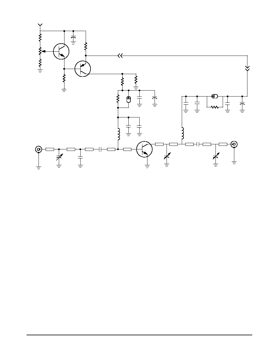
R7
Figure 1. Class AB Test Fixture Electrical Schematic
B1, B2
Ferrite Bead, P/N 5659065/3B, Ferroxcube
C1, C13
0.1
µ
F, Chip Capacitor, Kermet
C2
100
µ
F, 50 V, Electrolytic Capacitor, Mallory
C3, C5, C12
0.6≠4 pF, Variable Capacitor, Johanson, Gigatrim
C4, C11
10 pF, B Case Chip Capacitor, ATC
C6, C8
24 pF, B Case Chip Capacitor, ATC
C7, C9
75 pF, B Case Chip Capacitor, ATC
C10
0.4≠2.5 pF, Variable Capacitor, Johanson, Gigatrim
C14
470
µ
F, 63 V, Electrolytic Capacitor, Mallory
D1
Diode, Motorola (MUR3160T3)
L1, L4
12 Turns, 22 AWG, IDIA. 0.195
L2, L3
0.750
20 AWG
N1, N2
Type N Flange Mount RF Connector
MA/COM 3052≠1648≠10
R1, R2
130
, 1/8 W Chip Resistor, Rohm
R3, R4
100
, 1/8 W Chip Resistor, Rohm
R5, R8
10
, 1/2 W Resistor
R6, R7
10
, 1/8 W Chip Resistor, Rohm (10J)
Q1
Transistor, PNP Motorola (BD136)
Q2
Transistor, NPN Motorola (MJD47)
Board
30 Mil Glass Teflon
Æ
, Arlon GX≠0300≠55≠22,
r = 2.55
RF
INPUT
RF
OUT
DUT
Z8
Z1
Z2
Z3
Z4
Z5
Z6
Z7
VBB
VCC
Q2
Q1
D1
R2
C1
C2
R5
L1
R3
C6
C7
L2
C4
C3
C5
C8
C9
L4
C12
B2
C13
C14
R8
L4
C11
C10
R1
R4
B1
R6
+
+
MRF20030
4
MOTOROLA RF DEVICE DATA
B1, B2
Long Bead, Fair Rite
C1, C9, C13
0.6≠4 pF, Variable Capacitor, Johanson, Gigatrim
C2, C8
100
µ
F, 50 V, Electrolytic Capacitor, Mallory
C3, C10
18 pF B Case Chip Capacitor, ATC
C4
1.3 pF, B Case Chip Capacitor, ATC
C5, C11
24 pF, B Case Chip Capacitor, ATC
C6, C14
0.1
m
F, Chip Capacitor, Kermet
C7, C12
75 pF, B Case Chip Capacitor, ATC
C15
470
m
F, 63 V, Electrolytic Capacitor, Mallory
L1, L2
0.75 in., 20 AWG
N1, N2
Type N Flange Mount RF
Connector, MA/COM
Q1
Transistor, NPN, Motorola (BD135)
Q2
Transistor, PNP, Motorola (BD136)
R1
250
W,
Chip Resistor, 1/8 Watt, Rohm
R2
500
W
, 1/4 Watt, Potentiometer
R3
4.7 k
W
, Chip Resistor, 1/8 Watt, Rohm
R4
2 x 4.7 k
W
, Chip Resistor, 1/8 Watt, Rohm
R5
1.0
W
, 10 Watt, Resistor, DALE
R6
39
W
, 1 Watt, Resistor
R7, R9
4 x 39
W
, Chip Resistors, 1/8 Watt, Rohm
R8
75
W
, Chip Resistor, 1/8 Watt, Rohm
Board
30 Mil Glass Teflon
Æ
, Arlon GX≠0300≠55≠22,
r = 2.55
RF
OUTPUT
RF
INPUT
L2
L1
C10
C5
C7
C6
B1
R9
C9
N2
VCC
DUT
C1
C4
N1
C3
R1
R5
C2
Vsupply
Figure 2. Class A Test Fixture Electrical Schematic
C8
VCC
Z1
Z2
Z3
Z5
Z6
Z7
R4
R7
R6
R3
R2
Q1
Q2
R8
Z4
Z8
Z9
C11
C12
C14
C15
B2
C13
Z10
+
+
+

5
MRF20030
MOTOROLA RF DEVICE DATA
TYPICAL CHARACTERISTICS
G
pe
, POWER GAIN (dB)
G
pe
, GAIN (dB)
Figure 3. Output Power & Power Gain
versus Input Power
30
Pin, INPUT POWER (WATTS)
5
0
2
10
20
15
Figure 4. Output Power versus Frequency
0
1850
f, FREQUENCY (MHz)
40
20
5
1
3
5
30
P out
, OUTPUT
POWER (W
A
TTS)
1800
2000
0
P out
, OUTPUT
POWER (W
A
TTS)
25
11
10
9
8
G
pe
, GAIN (dB)
1900
1950
Figure 5. Intermodulation Distortion
versus Output Power
≠ 20
Pout, OUTPUT POWER (WATTS) PEP
≠ 70
20
Figure 6. Power Gain and Intermodulation
Distortion versus Supply Voltage
10.5
VCC, COLLECTOR SUPPLY VOLTAGE (Vdc)
9
10
30
40
8
IMD, INTERMODULA
TION
DIST
OR
TION
(dBc)
Figure 7. Intermodulation Distortion
versus Output Power
0.01
Pout, OUTPUT POWER (WATTS) PEP
≠ 45
≠ 60
10
≠ 35
Figure 8. Power Gain versus Output Power
Pout, OUTPUT POWER (WATTS) PEP
5
1.0
10
10
1.0
100
100
0.01
0
6
7
8
9.5
8.5
7.5
20
22
18
≠ 50
≠ 40
≠ 25
IMD, INTERMODULA
TION
DIST
OR
TION
(dBc)
≠45
≠35
IMD, INTERMODULA
TION
DIST
OR
TION
(dBc)
VCC = 26 Vdc
ICQ = 125 mA
f = 2000 MHz Single Tone
35
24
26
28
12
11.5
≠25
≠20
≠15
≠10
≠5
≠ 60
≠ 50
≠ 40
≠ 30
10
25
15
Pout = 30 W (PEP)
ICQ = 125 mA
f1 = 2000.0 MHz
f2 = 2000.1 MHz
IMD
Gpe
Pout
3rd Order
7th Order
5th Order
Pin = 3.5 W
VCC = 26 Vdc
f1 = 2000.0 MHz
f2 = 2000.1 MHz
250 mA
125 mA
ICQ = 75 mA
VCC = 26 Vdc
ICQ = 125 mA
f1 = 2000.0 MHz
f2 = 2000.1 MHz
4
≠ 55
15
5
25
35
75 mA
250 mA
125 mA
11.5
10.5
9.5
8.5
1.5 W
35
2.5 W
10
11
Gpe
≠40
≠30
≠ 30
11
9
ICQ = 400 mA
VCC = 26 Vdc
f1 = 2000.0 MHz
f2 = 2000.1 MHz
0.1
0.1
400 mA
VCC = 26 Vdc
ICQ = 125 mA