 | ÐлекÑÑоннÑй компоненÑ: MTB1306 | СкаÑаÑÑ:  PDF PDF  ZIP ZIP |
Äîêóìåíòàöèÿ è îïèñàíèÿ www.docs.chipfind.ru
1
Motorola TMOS Power MOSFET Transistor Device Data
Advance Information
HDTMOS E-FET
.
TM
High Density Power FET
D2PAK for Surface Mount
NChannel EnhancementMode Silicon Gate
The D2PAK package has the capability of housing a larger die
than any existing surface mount package which allows it to be used
in applications that require the use of surface mount components
with higher power and lower RDS(on) capabilities. This advanced
highcell density HDTMOS power FET is designed to withstand
high energy in the avalanche and commutation modes. This new
energy efficient design also offers a draintosource diode with fast
recovery time. Designed for low voltage, high speed switching
applications in power supplies, converters and PWM motor
controls, these devices are particularly well suited for bridge circuits
where diode speed and commutating safe operating areas are
critical and offer additional safety margin against unexpected
voltage transients.
·
Avalanche Energy Specified
·
SourcetoDrain Diode Recovery Time Comparable
to a Discrete Fast Recovery Diode
·
Diode is Characterized for Use in Bridge Circuits
·
IDSS and VDS(on) Specified at Elevated Temperature
·
Short Heatsink Tab Manufactured -- Not Sheared
·
Specially Designed Leadframe for Maximum Power Dissipation
·
Surface Mount Package Available in 16 mm, 13inch/2500
Unit Tape & Reel, Add T4 Suffix to Part Number
MAXIMUM RATINGS
(TC = 25
°
C unless otherwise noted)
Rating
Symbol
Value
Unit
DraintoSource Voltage
VDSS
30
Vdc
DraintoGate Voltage (RGS = 1.0 M
)
VDGR
30
Vdc
GatetoSource Voltage -- Continuous
-- NonRepetitive (tp
10 ms)
VGS
VGSM
±
20
±
20
Vdc
Vpk
Drain Current
-- Continuous
-- Continuous @ 100
°
C
-- Single Pulse (tp
10
µ
s)
ID
ID
IDM
75
59
225
Adc
Apk
Total Power Dissipation
Derate above 25
°
C
Total Power Dissipation @ TA = 25
°
C (1)
PD
150
1.2
2.5
Watts
W/
°
C
Watts
Operating and Storage Temperature Range
TJ, Tstg
55 to 150
°
C
Single Pulse DraintoSource Avalanche Energy -- Starting TJ = 25
°
C
(VDD = 25 Vdc, VGS = 10 Vdc, Peak IL = 75 Apk, L = 0.1 mH, RG = 25
)
EAS
280
mJ
Thermal Resistance -- JunctiontoCase
-- JunctiontoAmbient
-- JunctiontoAmbient (1)
R
JC
R
JA
R
JA
0.8
62.5
50
°
C/W
Maximum Lead Temperature for Soldering Purposes, 1/8
from Case for 5.0 seconds
TL
260
°
C
(1) When surface mounted to an FR4 board using the minimum recommended pad size.
This document contains information on a new product. Specifications and information herein are subject to change without notice.
EFET and HDTMOS are trademarks of Motorola, Inc.
Order this document
by MTB1306/D
MOTOROLA
SEMICONDUCTOR TECHNICAL DATA
MTB1306
TMOS POWER FET
75 AMPERES
30 VOLTS
RDS(on) = 0.0065 OHM
CASE 418B03
D2PAK
©
Motorola, Inc. 1997

MTB1306
2
Motorola TMOS Power MOSFET Transistor Device Data
ELECTRICAL CHARACTERISTICS
(TJ = 25
°
C unless otherwise noted)
Characteristic
Symbol
Min
Typ
Max
Unit
OFF CHARACTERISTICS
DraintoSource Breakdown Voltage
(VGS = 0 Vdc, ID = 0.25 mAdc)
V(BR)DSS
30
--
--
Vdc
Zero Gate Voltage Drain Current
(VDS = 30 Vdc, VGS = 0 Vdc)
(VDS = 30 Vdc, VGS = 0 Vdc, TJ = 125
°
C)
IDSS
--
--
--
--
10
100
µ
Adc
GateBody Leakage Current (VGS =
±
20 Vdc, VDS = 0 Vdc)
IGSS
--
--
100
nAdc
ON CHARACTERISTICS(1)
Gate Threshold Voltage
(VDS = VGS, ID = 250
µ
Adc)
VGS(th)
1.0
1.5
2.0
Vdc
Static DraintoSource OnResistance
(VGS = 10 Vdc, ID = 38 Adc)
(VGS = 5.0 Vdc, ID = 38 Adc)
RDS(on)
--
--
5.8
7.4
6.5
8.5
m
W
DraintoSource OnVoltage
(VGS = 10 Vdc, ID = 75 Adc)
(VGS = 10 Vdc, ID = 38 Adc, TJ = 150
°
C)
VDS(on)
--
--
0.44
--
0.5
0.38
Vdc
Forward Transconductance (VDS = 3.0 Vdc, ID = 20 Adc)
gFS
15
55
--
mhos
DYNAMIC CHARACTERISTICS
Input Capacitance
(V
25 Vdc V
0 Vdc
Ciss
--
2560
3584
pF
Output Capacitance
(VDS = 25 Vdc, VGS = 0 Vdc,
f = 1.0 MHz)
Coss
--
1305
1827
Transfer Capacitance
f = 1.0 MHz)
Crss
--
386
772
SWITCHING CHARACTERISTICS(2)
TurnOn Delay Time
(V
15 Vd
I
75 Ad
td(on)
--
17
35
ns
Rise Time
(VDD = 15 Vdc, ID = 75 Adc,
VGS = 5 0 Vdc
tr
--
170
340
TurnOff Delay Time
VGS = 5.0 Vdc,
RG = 4.7
)
td(off)
--
68
136
Fall Time
G
)
tf
--
145
290
Gate Charge
(V
24 Vd
I
75 Ad
QT
--
50
70
nC
(VDS = 24 Vdc, ID = 75 Adc,
Q1
--
8.3
--
( DS
, D
,
VGS = 5.0 Vdc)
Q2
--
25.3
--
Q3
--
17.2
--
SOURCEDRAIN DIODE CHARACTERISTICS
Forward OnVoltage
(IS = 20 Adc, VGS = 0 Vdc)
(IS = 20 Adc, VGS = 0 Vdc, TJ = 125
°
C)
VSD
--
--
0.75
0.64
1.1
--
Vdc
Reverse Recovery Time
(I
20 Ad
V
0 Vd
trr
--
84
--
ns
(IS = 20 Adc, VGS = 0 Vdc,
ta
--
35
--
( S
,
GS
,
dIS/dt = 100 A/
µ
s)
tb
--
53
--
Reverse Recovery Stored Charge
QRR
--
0.13
--
µ
C
(1) Pulse Test: Pulse Width
300
µ
s, Duty Cycle
2%.
(2) Switching characteristics are independent of operating junction temperature.
MTB1306
3
Motorola TMOS Power MOSFET Transistor Device Data
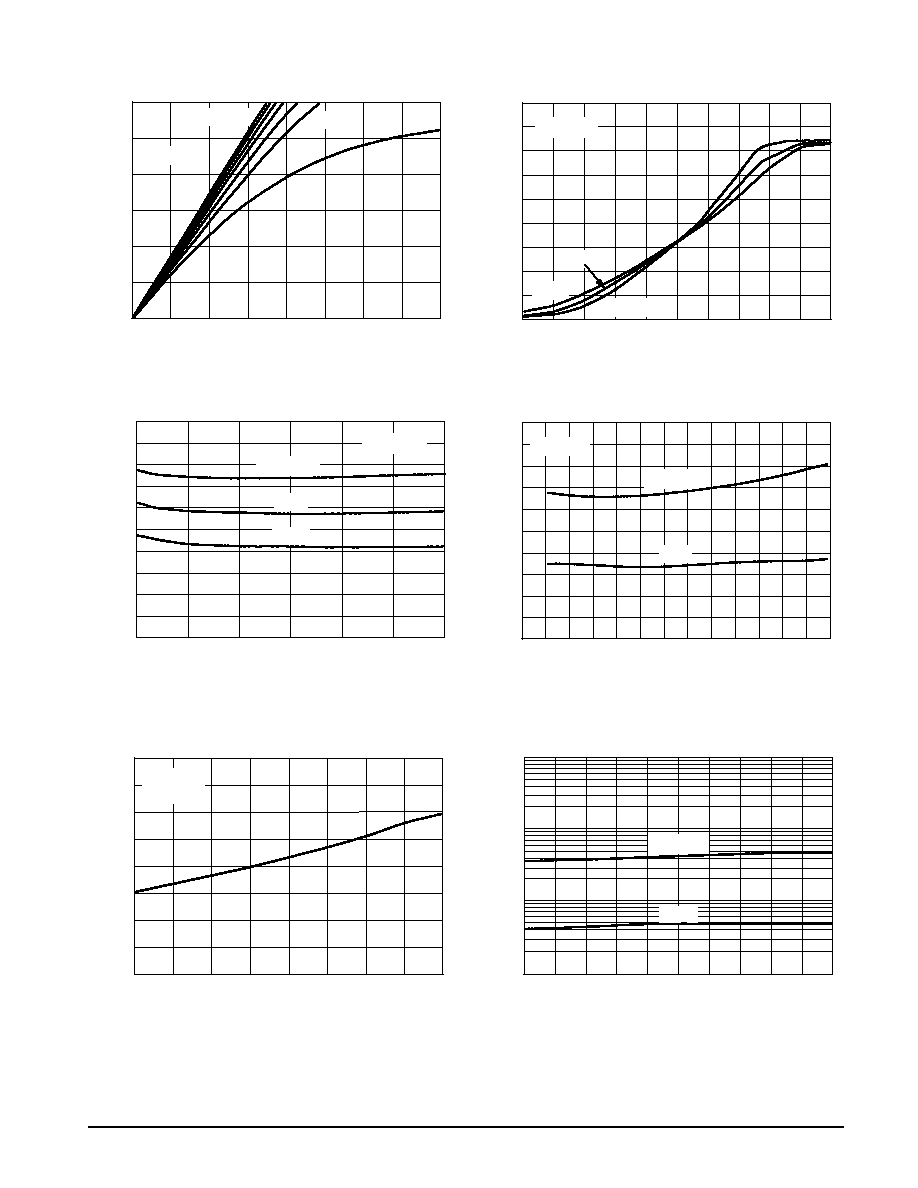
TYPICAL ELECTRICAL CHARACTERISTICS
R
DS(on)
, DRAINT
OSOURCE
RESIST
ANCE
(NORMALIZED)
R
DS(on)
, DRAINT
OSOURCE
ONRESIST
ANCE
(OHMS)
R
DS(on)
, DRAINT
OSOURCE
RESIST
ANCE
(OHMS)
0
0.25
0.75
1.25
1.5
2.0
0
75
125
150
VDS, DRAINTOSOURCE VOLTAGE (VOLTS)
Figure 1. OnRegion Characteristics
I D
, DRAIN CURRENT
(AMPS)
I D
, DRAIN CURRENT
(AMPS)
VGS, GATETOSOURCE VOLTAGE (VOLTS)
Figure 2. Transfer Characteristics
20
40
80
0
0.001
0.003
0.005
0.007
20
40
90
0.004
0.005
0.006
0.007
0.008
ID, DRAIN CURRENT (AMPS)
Figure 3. OnResistance versus Drain Current
and Temperature
ID, DRAIN CURRENT (AMPS)
Figure 4. OnResistance versus Drain Current
and Gate Voltage
50
0
0.5
2.0
10
15
20
25
30
10
100
1000
10,000
TJ, JUNCTION TEMPERATURE (
°
C)
Figure 5. OnResistance Variation with
Temperature
VDS, DRAINTOSOURCE VOLTAGE (VOLTS)
Figure 6. DrainToSource Leakage
Current versus Voltage
I DSS
, LEAKAGE (nA)
25
0
25
50
75
100
125
150
TJ = 25
°
C
VDS
10 V
TJ = 55
°
C
TJ = 100
°
C
TJ = 25
°
C
50
100
0.5
1.0
1.75
25
VGS = 10 V
0
60
160
180
40
140
20
2.0
2.5
3.0
3.5
4.0
4.5
0.006
0.004
0.002
60
100
140
60
80
100
1.5
VGS = 10 V
ID = 38 A
1.0
5.0
TJ = 125
°
C
100
°
C
0.008
0.009
0.010
0.009
5.0 V
4.0 V
120
100
80
125
°
C
25
°
C
120
25
°
C
55
°
C
30
50
70
150
120
140
130
110
VGS = 5.0 V
10 V
VGS
10 V
MTB1306
4
Motorola TMOS Power MOSFET Transistor Device Data
POWER MOSFET SWITCHING
Switching behavior is most easily modeled and predicted
by recognizing that the power MOSFET is charge controlled.
The lengths of various switching intervals (
t) are deter-
mined by how fast the FET input capacitance can be charged
by current from the generator.
The published capacitance data is difficult to use for calculat-
ing rise and fall because draingate capacitance varies
greatly with applied voltage. Accordingly, gate charge data is
used. In most cases, a satisfactory estimate of average input
current (IG(AV)) can be made from a rudimentary analysis of
the drive circuit so that
t = Q/IG(AV)
During the rise and fall time interval when switching a resis-
tive load, VGS remains virtually constant at a level known as
the plateau voltage, VSGP. Therefore, rise and fall times may
be approximated by the following:
tr = Q2 x RG/(VGG VGSP)
tf = Q2 x RG/VGSP
where
VGG = the gate drive voltage, which varies from zero to VGG
RG = the gate drive resistance
and Q2 and VGSP are read from the gate charge curve.
During the turnon and turnoff delay times, gate current is
not constant. The simplest calculation uses appropriate val-
ues from the capacitance curves in a standard equation for
voltage change in an RC network. The equations are:
td(on) = RG Ciss In [VGG/(VGG VGSP)]
td(off) = RG Ciss In (VGG/VGSP)
The capacitance (Ciss) is read from the capacitance curve at
a voltage corresponding to the offstate condition when cal-
culating td(on) and is read at a voltage corresponding to the
onstate when calculating td(off).
At high switching speeds, parasitic circuit elements com-
plicate the analysis. The inductance of the MOSFET source
lead, inside the package and in the circuit wiring which is
common to both the drain and gate current paths, produces a
voltage at the source which reduces the gate drive current.
The voltage is determined by Ldi/dt, but since di/dt is a func-
tion of drain current, the mathematical solution is complex.
The MOSFET output capacitance also complicates the
mathematics. And finally, MOSFETs have finite internal gate
resistance which effectively adds to the resistance of the
driving source, but the internal resistance is difficult to mea-
sure and, consequently, is not specified.
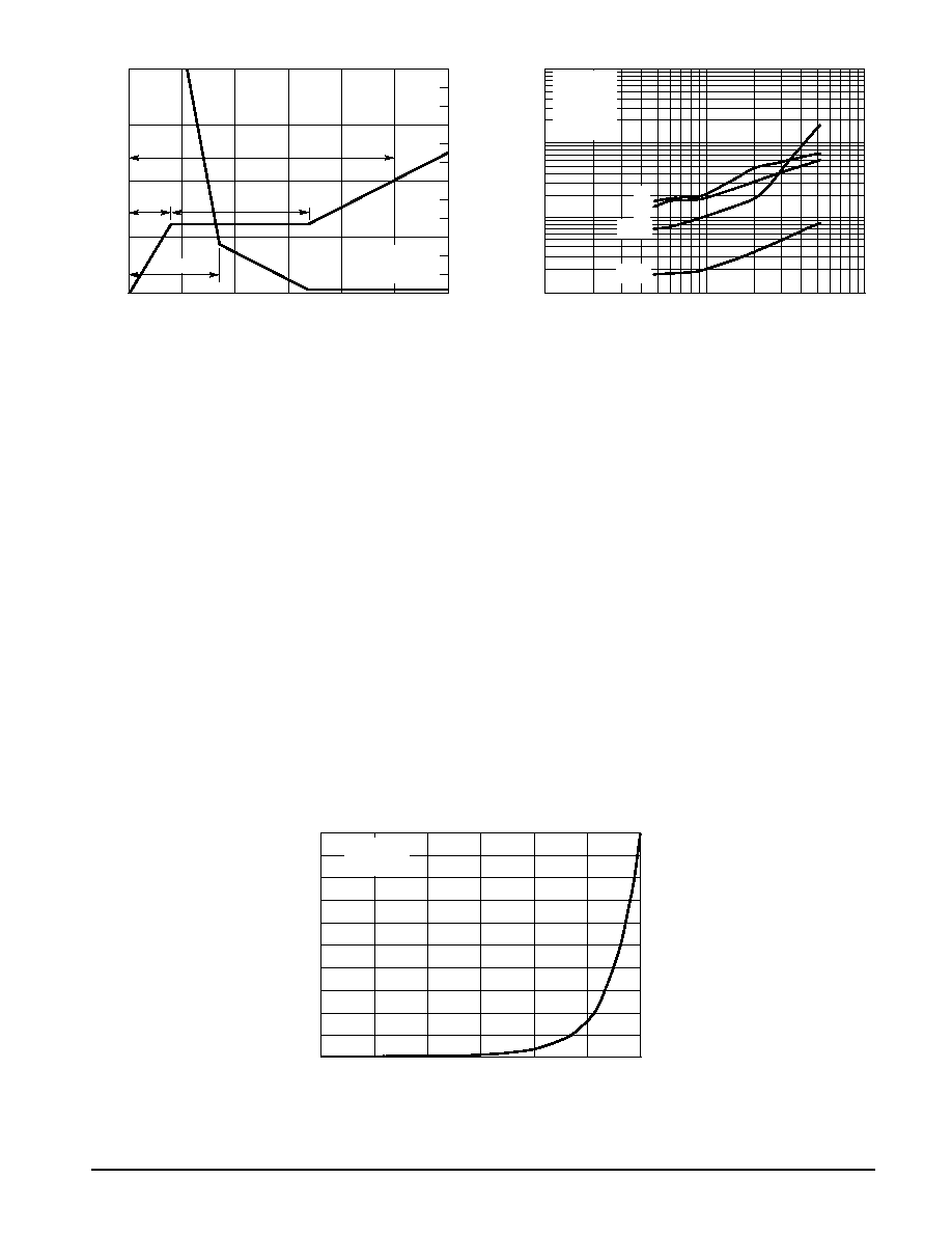
The resistive switching time variation versus gate resis-
tance (Figure 9) shows how typical switching performance is
affected by the parasitic circuit elements. If the parasitics
were not present, the slope of the curves would maintain a
value of unity regardless of the switching speed. The circuit
used to obtain the data is constructed to minimize common
inductance in the drain and gate circuit loops and is believed
readily achievable with board mounted components. Most
power electronic loads are inductive; the data in the figure is
taken with a resistive load, which approximates an optimally
snubbed inductive load. Power MOSFETs may be safely op-
erated into an inductive load; however, snubbing reduces
switching losses.
10
0
10
15
20
25
VGS OR VDS, GATETOSOURCE OR DRAINTOSOURCE
VOLTAGE (VOLTS)
C, CAP
ACIT
ANCE
(pF)
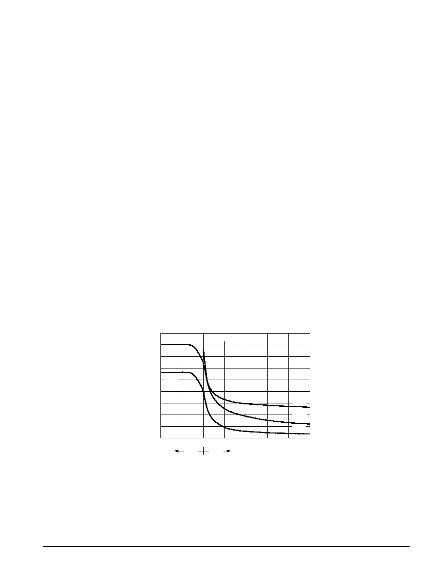
Figure 7. Capacitance Variation
7000
5000
3000
1000
0
VGS
VDS
VDS = 0 V
VGS = 0 V
6000
4000
2000
5.0
5.0
Ciss
Coss
Ciss
Crss
Crss
8000
9000
MTB1306
5
Motorola TMOS Power MOSFET Transistor Device Data
Figure 8. GateToSource and DrainToSource
Voltage versus Total Charge
Figure 9. Resistive Switching Time
Variation versus Gate Resistance
RG, GATE RESISTANCE (OHMS)
1.0
10
100
10,000
100
t, TIME
(ns)
tr
tf
td(off)
td(on)
1000
VDD = 15 V
ID = 75 A
VGS = 5.0 V
TJ = 25
°
C
10
18
V
GS
, GA
TET
OSOURCE
VOL
T
AGE
(VOL
TS)
15
12
9.0
0
7.5
5.0
0
QG, TOTAL GATE CHARGE (nC)
V
DS
, DRAINT
OSOURCE
VOL
T
AGE
(VOL
TS)
10
10
20
30
40
TJ = 25
°
C
ID = 75 A
VDS
VGS
60
0
Q1
Q2
QT
Q3
6.0
3.0
50
2.5
DRAINTOSOURCE DIODE CHARACTERISTICS
The switching characteristics of a MOSFET body diode
are very important in systems using it as a freewheeling or
commutating diode. Of particular interest are the reverse re-
covery characteristics which play a major role in determining
switching losses, radiated noise, EMI and RFI.
System switching losses are largely due to the nature of
the body diode itself. The body diode is a minority carrier de-
vice, therefore it has a finite reverse recovery time, trr, due to
the storage of minority carrier charge, QRR, as shown in the
typical reverse recovery wave form of Figure 15. It is this
stored charge that, when cleared from the diode, passes
through a potential and defines an energy loss. Obviously,
repeatedly forcing the diode through reverse recovery further
increases switching losses. Therefore, one would like a
diode with short trr and low QRR specifications to minimize
these losses.
The abruptness of diode reverse recovery effects the
amount of radiated noise, voltage spikes, and current ring-
ing. The mechanisms at work are finite irremovable circuit
parasitic inductances and capacitances acted upon by high
di/dts. The diode's negative di/dt during ta is directly con-
trolled by the device clearing the stored charge. However,
the positive di/dt during tb is an uncontrollable diode charac-
teristic and is usually the culprit that induces current ringing.
Therefore, when comparing diodes, the ratio of tb/ta serves
as a good indicator of recovery abruptness and thus gives a
comparative estimate of probable noise generated. A ratio of
1 is considered ideal and values less than 0.5 are considered
snappy.
Compared to Motorola standard cell density low voltage
MOSFETs, high cell density MOSFET diodes are faster
(shorter trr), have less stored charge and a softer reverse re-
covery characteristic. The softness advantage of the high
cell density diode means they can be forced through reverse
recovery at a higher di/dt than a standard cell MOSFET
diode without increasing the current ringing or the noise gen-
erated. In addition, power dissipation incurred from switching
the diode will be less due to the shorter recovery time and
lower switching losses.
0.75
0.50
0.55
0.60
0.65
0
4.0
10
12
VSD, SOURCETODRAIN VOLTAGE (VOLTS)
I S
, SOURCE CURRENT
(AMPS)
VGS = 0 V
TJ = 25
°
C
Figure 10. Diode Forward Voltage versus Current
2.0
6.0
0.70
8.0
0.45
20
16
18
14