
1
Motorola TMOS Power MOSFET Transistor Device Data
Designer's
TM
Data Sheet
HDTMOS E-FET
.
TM
High Energy Power FET
D2PAK for Surface Mount
NнChannel EnhancementнMode Silicon Gate
The D2PAK package has the capability of housing a larger die
than any existing surface mount package which allows it to be used
in applications that require the use of surface mount components
with higher power and lower RDS(on) capabilities. This advanced
highнcell density HDTMOS power FET is designed to withstand
high energy in the avalanche and commutation modes. This new
energy efficient design also offers a drainнtoнsource diode with a
fast recovery time. Designed for low voltage, high speed switching
applications in power supplies, converters and PWM motor
controls, these devices are particularly well suited for bridge circuits
where diode speed and commutating safe operating areas are
critical and offer additional safety margin against unexpected
voltage transients.
╖
Avalanche Energy Specified
╖
SourceнtoнDrain Diode Recovery Time Comparable to a
Discrete Fast Recovery Diode
╖
Diode is Characterized for Use in Bridge Circuits
╖
IDSS and VDS(on) Specified at Elevated Temperature
╖
Short Heatsink Tab Manufactured -- Not Sheared
╖
Specially Designed Leadframe for Maximum Power Dissipation
╖
Available in 24 mm 13нinch/800 Unit Tape & Reel, Add T4 Suffix to Part Number
MAXIMUM RATINGS
(TC = 25
░
C unless otherwise noted)
Rating
Symbol
Value
Unit
DrainнtoнSource Voltage
VDSS
60
Vdc
DrainнtoнGate Voltage (RGS = 1.0 M
)
VDGR
60
Vdc
GateнtoнSource Voltage -- Continuous
GateнtoнSource Voltage
-- NonнRepetitive (tp
10 ms)
VGS
VGSM
▒
20
▒
30
Vdc
Vpk
Drain Current -- Continuous
Drain Current
-- Continuous @ 100
░
C
Drain Current
-- Single Pulse (tp
10
╡
s)
ID
ID
IDM
75
50
225
Adc
Apk
Total Power Dissipation
Derate above 25
░
C
Total Power Dissipation @ TC = 25
░
C (1)
PD
125
1.0
2.5
Watts
W/
░
C
Watts
Operating and Storage Temperature Range
н 55 to 150
░
C
Single Pulse DrainнtoнSource Avalanche Energy -- Starting TJ = 25
░
C
(VDD = 25 Vdc, VGS = 10 Vdc, IL = 75 Apk, L = 0.177 mH, RG = 25
)
EAS
500
mJ
Thermal Resistance -- Junction to Case
Thermal Resistance
-- Junction to Ambient
Thermal Resistance
-- Junction to Ambient (1)
R
JC
R
JA
R
JA
1.0
62.5
50
░
C/W
Maximum Lead Temperature for Soldering Purposes, 1/8
from case for 10 seconds
TL
260
░
C
(1) When surface mounted to an FR4 board using the minimum recommended pad size.
Designer's Data for "Worst Case" Conditions -- The Designer's Data Sheet permits the design of most circuits entirely from the information presented. SOA Limit
curves -- representing boundaries on device characteristics -- are given to facilitate "worst case" design.
EнFET, Designer's and HDTMOS are trademarks of Motorola, Inc.
TMOS is a registered trademark of Motorola, Inc. Thermal Clad is a trademark of the Bergquist Company.
Preferred devices are Motorola recommended choices for future use and best overall value.
REV 1
Order this document
by MTB75N06HD/D
MOTOROLA
SEMICONDUCTOR TECHNICAL DATA
й
Motorola, Inc. 1995
D
S
G
MTB75N06HD
TMOS POWER FET
75 AMPERES
60 VOLTS
RDS(on) = 10 mOHM
Motorola Preferred Device
TM
CASE 418Bн02, Style 2
D2PAK

MTB75N06HD
2
Motorola TMOS Power MOSFET Transistor Device Data
ELECTRICAL CHARACTERISTICS
(TJ = 25
░
C unless otherwise noted)
Characteristic
Symbol
Min
Typ
Max
Unit
OFF CHARACTERISTICS
DrainнSource Breakdown Voltage
(Cpk
2.0) (3)
(VGS = 0 Vdc, ID = 250
╡
Adc)
Temperature Coefficient (Positive)
V(BR)DSS
60
--
68
60.4
--
--
Vdc
mV/
░
C
Zero Gate Voltage Drain Current
(VDS = 60 Vdc, VGS = 0 Vdc)
(VDS = 60 Vdc, VGS = 0 Vdc, TJ = 125
░
C)
IDSS
--
--
--
--
10
100
╡
Adc
GateнBody Leakage Current (VGS =
▒
20 Vdc, VDS = 0 V)
IGSS
--
5.0
100
nAdc
ON CHARACTERISTICS (1)
Gate Threshold Voltage
(Cpk
5.0) (3)
(VDS = VGS, ID = 250
╡
Adc)
Temperature Coefficient (Negative)
VGS(th)
2.0
--
3.0
8.38
4.0
--
Vdc
mV/
░
C
Static DrainнSource OnнResistance
(Cpk
2.0) (3)
(VGS = 10 Vdc, ID = 37.5 Adc)
RDS(on)
--
8.3
10
m
DrainнSource OnнVoltage (VGS = 10 Vdc)
(ID = 75 Adc)
(ID = 37.5 Adc, TJ = 125
░
C)
VDS(on)
--
--
0.7
0.53
0.9
0.8
Vdc
Forward Transconductance (VDS = 15 Vdc, ID = 37.5 Adc)
gFS
15
32
--
mhos
DYNAMIC CHARACTERISTICS
Input Capacitance
(VDS = 25 Vdc, VGS = 0 Vdc,
f = 1.0 MHz)
Ciss
--
2800
3920
pF
Output Capacitance
(VDS = 25 Vdc, VGS = 0 Vdc,
f = 1.0 MHz)
Coss
--
928
1300
Reverse Transfer Capacitance
f = 1.0 MHz)
Crss
--
180
252
SWITCHING CHARACTERISTICS (2)
TurnнOn Delay Time
(VDS = 30 Vdc, ID = 75 Adc,
VGS = 10 Vdc,
RG = 9.1
)
td(on)
--
18
26
ns
Rise Time
(VDS = 30 Vdc, ID = 75 Adc,
VGS = 10 Vdc,
RG = 9.1
)
tr
--
218
306
TurnнOff Delay Time
VGS = 10 Vdc,
RG = 9.1
)
td(off)
--
67
94
Fall Time
G = 9.1
)
tf
--
125
175
Gate Charge
(VDS = 48 Vdc, ID = 75 Adc,
VGS = 10 Vdc)
QT
--
71
100
nC
(VDS = 48 Vdc, ID = 75 Adc,
VGS = 10 Vdc)
Q1
--
16.3
--
(VDS = 48 Vdc, ID = 75 Adc,
VGS = 10 Vdc)
Q2
--
31
--
Q3
--
29.4
--
SOURCEнDRAIN DIODE CHARACTERISTICS
Forward OnнVoltage
(IS = 75 Adc, VGS = 0 Vdc)
(IS = 75 Adc, VGS = 0 Vdc, TJ = 125
░
C)
VSD
--
--
0.97
0.88
1.1
--
Vdc
Reverse Recovery Time
(IS = 75 Adc,
dIS/dt = 100 A/
╡
s)
trr
--
56
--
ns
(IS = 75 Adc,
dIS/dt = 100 A/
╡
s)
ta
--
44
--
(IS = 75 Adc,
dIS/dt = 100 A/
╡
s)
tb
--
12
--
Reverse Recovery Stored Charge
QRR
--
0.103
--
╡
C
INTERNAL PACKAGE INDUCTANCE
Internal Drain Inductance
(Measured from contact screw on tab to center of die)
(Measured from the drain lead 0.25
from package to center of die)
LD
--
3.5
--
nH
Internal Source Inductance
(Measured from the source lead 0.25
from package to source bond pad)
LS
--
7.5
--
nH
(1) Pulse Test: Pulse Width
300
╡
s, Duty Cycle
2%.
(2) Switching characteristics are independent of operating junction temperature.
(3) Reflects typical values.
Cpk =
Max limit н Typ
3 x SIGMA

MTB75N06HD
3
Motorola TMOS Power MOSFET Transistor Device Data
TYPICAL ELECTRICAL CHARACTERISTICS
R
DS(on)
, DRAINнT
OнSOURCE RESIST
ANCE
(NORMALIZED)
I DSS
, LEAKAGE (nA)
VDS, DRAINнTOнSOURCE VOLTAGE (VOLTS)
TJ, JUNCTION TEMPERATURE (
░
C)
VDS, DRAINнTOнSOURCE VOLTAGE (VOLTS)
VGS, GATEнTOнSOURCE VOLTAGE (VOLTS)
I D
, DRAIN CURRENT
(AMPS)
I D
, DRAIN CURRENT
(AMPS)
0
0.5
1
Figure 1. OnнRegion Characteristics
Figure 2. Transfer Characteristics
Figure 3. OnнResistance versus Drain Current
and Temperature
Figure 4. OnнResistance versus Drain Current
and Gate Voltage
1
1000
Figure 5. OnнResistance Variation with
Temperature
Figure 6. DrainнToнSource Leakage
Current versus Voltage
VDS
10 V
TJ = н 55
░
C
25
░
C
н 50
н 25
0
25
50
75
100
125
150
0
10
20
60
40
VGS = 0 V
TJ = 125
░
C
VGS = 10 V
ID = 37.5 A
100
30
9 V
TJ = 25
░
C
100
░
C
150
0
2
1.5
100
░
C
1.9
1.6
1.3
1
0.7
2
5
4
7
3
6
8
125
100
75
50
25
VGS = 10 V
8 V
7 V
6 V
5 V
150
0
125
100
75
50
25
10
50
25
░
C
R
DS(on)
, DRAINнT
OнSOURCE RESIST
ANCE (OHMS)
R
DS(on)
, DRAINнT
OнSOURCE RESIST
ANCE (OHMS)
ID, DRAIN CURRENT (AMPS)
ID, DRAIN CURRENT (AMPS)
0
50
150
TJ = 25
░
C
25
75
15 V
0.016
0.012
0.009
0.007
0.006
0.014
0.012
0.010
0.008
0.006
0.004
100
125
TJ = 25
░
C
VGS = 10 V
TJ = 100
░
C
25
░
C
н 55
░
C
VGS = 10 V
0.010
0.008
0
50
150
25
75
100
125
0.011
MTB75N06HD
4
Motorola TMOS Power MOSFET Transistor Device Data
POWER MOSFET SWITCHING
Switching behavior is most easily modeled and predicted
by recognizing that the power MOSFET is charge controlled.
The lengths of various switching intervals (
t) are deter-
mined by how fast the FET input capacitance can be charged
by current from the generator.
The published capacitance data is difficult to use for calculat-
ing rise and fall because drainнgate capacitance varies
greatly with applied voltage. Accordingly, gate charge data is
used. In most cases, a satisfactory estimate of average input
current (IG(AV)) can be made from a rudimentary analysis of
the drive circuit so that
t = Q/IG(AV)
During the rise and fall time interval when switching a resis-
tive load, VGS remains virtually constant at a level known as
the plateau voltage, VSGP. Therefore, rise and fall times may
be approximated by the following:
tr = Q2 x RG/(VGG н VGSP)
tf = Q2 x RG/VGSP
where
VGG = the gate drive voltage, which varies from zero to VGG
RG = the gate drive resistance
and Q2 and VGSP are read from the gate charge curve.
During the turnнon and turnнoff delay times, gate current is
not constant. The simplest calculation uses appropriate val-
ues from the capacitance curves in a standard equation for
voltage change in an RC network. The equations are:
td(on) = RG Ciss In [VGG/(VGG н VGSP)]
td(off) = RG Ciss In (VGG/VGSP)
The capacitance (Ciss) is read from the capacitance curve at
a voltage corresponding to the offнstate condition when cal-
culating td(on) and is read at a voltage corresponding to the
onнstate when calculating td(off).
At high switching speeds, parasitic circuit elements com-
plicate the analysis. The inductance of the MOSFET source
lead, inside the package and in the circuit wiring which is
common to both the drain and gate current paths, produces a
voltage at the source which reduces the gate drive current.
The voltage is determined by Ldi/dt, but since di/dt is a func-
tion of drain current, the mathematical solution is complex.
The MOSFET output capacitance also complicates the
mathematics. And finally, MOSFETs have finite internal gate
resistance which effectively adds to the resistance of the
driving source, but the internal resistance is difficult to mea-
sure and, consequently, is not specified.
The resistive switching time variation versus gate resis-
tance (Figure 9) shows how typical switching performance is
affected by the parasitic circuit elements. If the parasitics
were not present, the slope of the curves would maintain a
value of unity regardless of the switching speed. The circuit
used to obtain the data is constructed to minimize common
inductance in the drain and gate circuit loops and is believed
readily achievable with board mounted components. Most
power electronic loads are inductive; the data in the figure is
taken with a resistive load, which approximates an optimally
snubbed inductive load. Power MOSFETs may be safely op-
erated into an inductive load; however, snubbing reduces
switching losses.
GATEнTOнSOURCE OR DRAINнTOнSOURCE VOLTAGE (VOLTS)
C, CAP
ACIT
ANCE (pF)
Figure 7. Capacitance Variation
10
0
10
15
20
25
VGS
VDS
5
5
VDS = 0 V
Ciss
Crss
VGS = 0 V
TJ = 25
░
C
Ciss
Coss
Crss
7000
6000
5000
4000
3000
2000
1000
0

MTB75N06HD
5
Motorola TMOS Power MOSFET Transistor Device Data
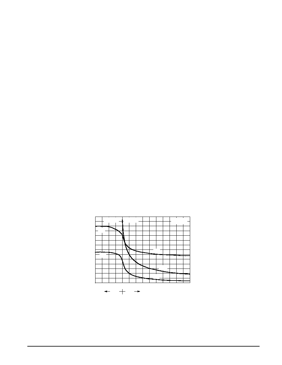
QT, TOTAL GATE CHARGE (nC)
RG, GATE RESISTANCE (Ohms)
t,
TIME (ns)
V
DS
, DRAINнT
OнSOURCE VOL
T
AGE (VOL
TS)
V
GS
, GA
TEнT
OнSOURCE VOL
T
AGE (VOL
TS)
Figure 8. GateнToнSource and DrainнToнSource
Voltage versus Total Charge
1
10
100
10
100
1000
VDD = 30 V
ID = 75 A
VGS = 10 V
TJ = 25
░
C
tr
tf
td(on)
td(off)
Figure 9. Resistive Switching Time
Variation versus Gate Resistance
0
10
30
50
60
80
20
40
10
6
2
0
8
4
12
60
50
40
30
10
20
0
QT
Q2
VGS
ID = 75 A
TJ = 25
░
C
VDS
Q3
Q1
70
DRAINнTOнSOURCE DIODE CHARACTERISTICS
The switching characteristics of a MOSFET body diode
are very important in systems using it as a freewheeling or
commutating diode. Of particular interest are the reverse re-
covery characteristics which play a major role in determining
switching losses, radiated noise, EMI and RFI.
System switching losses are largely due to the nature of
the body diode itself. The body diode is a minority carrier de-
vice, therefore it has a finite reverse recovery time, trr, due to
the storage of minority carrier charge, QRR, as shown in the
typical reverse recovery wave form of Figure 12. It is this
stored charge that, when cleared from the diode, passes
through a potential and defines an energy loss. Obviously,
repeatedly forcing the diode through reverse recovery further
increases switching losses. Therefore, one would like a
diode with short trr and low QRR specifications to minimize
these losses.
The abruptness of diode reverse recovery effects the
amount of radiated noise, voltage spikes, and current ring-
ing. The mechanisms at work are finite irremovable circuit
parasitic inductances and capacitances acted upon by high
di/dts. The diode's negative di/dt during ta is directly con-
trolled by the device clearing the stored charge. However,
the positive di/dt during tb is an uncontrollable diode charac-
teristic and is usually the culprit that induces current ringing.
Therefore, when comparing diodes, the ratio of tb/ta serves
as a good indicator of recovery abruptness and thus gives a
comparative estimate of probable noise generated. A ratio of
1 is considered ideal and values less than 0.5 are considered
snappy.
Compared to Motorola standard cell density low voltage
MOSFETs, high cell density MOSFET diodes are faster
(shorter trr), have less stored charge and a softer reverse re-
covery characteristic. The softness advantage of the high
cell density diode means they can be forced through reverse
recovery at a higher di/dt than a standard cell MOSFET
diode without increasing the current ringing or the noise gen-
erated. In addition, power dissipation incurred from switching
the diode will be less due to the shorter recovery time and
lower switching losses.
I S
, SOURCE CURRENT
(AMPS)
VSD, SOURCEнTOнDRAIN VOLTAGE (VOLTS)
Figure 10. Diode Forward Voltage versus Current
0
50
75
25
0.5
0.58
0.66
0.74
0.82
0.98
VGS = 0 V
TJ = 25
░
C
0.9