 | ÐлекÑÑоннÑй компоненÑ: MTP55N06Z | СкаÑаÑÑ:  PDF PDF  ZIP ZIP |
Äîêóìåíòàöèÿ è îïèñàíèÿ www.docs.chipfind.ru
1
Motorola TMOS Power MOSFET Transistor Device Data
Advance Information
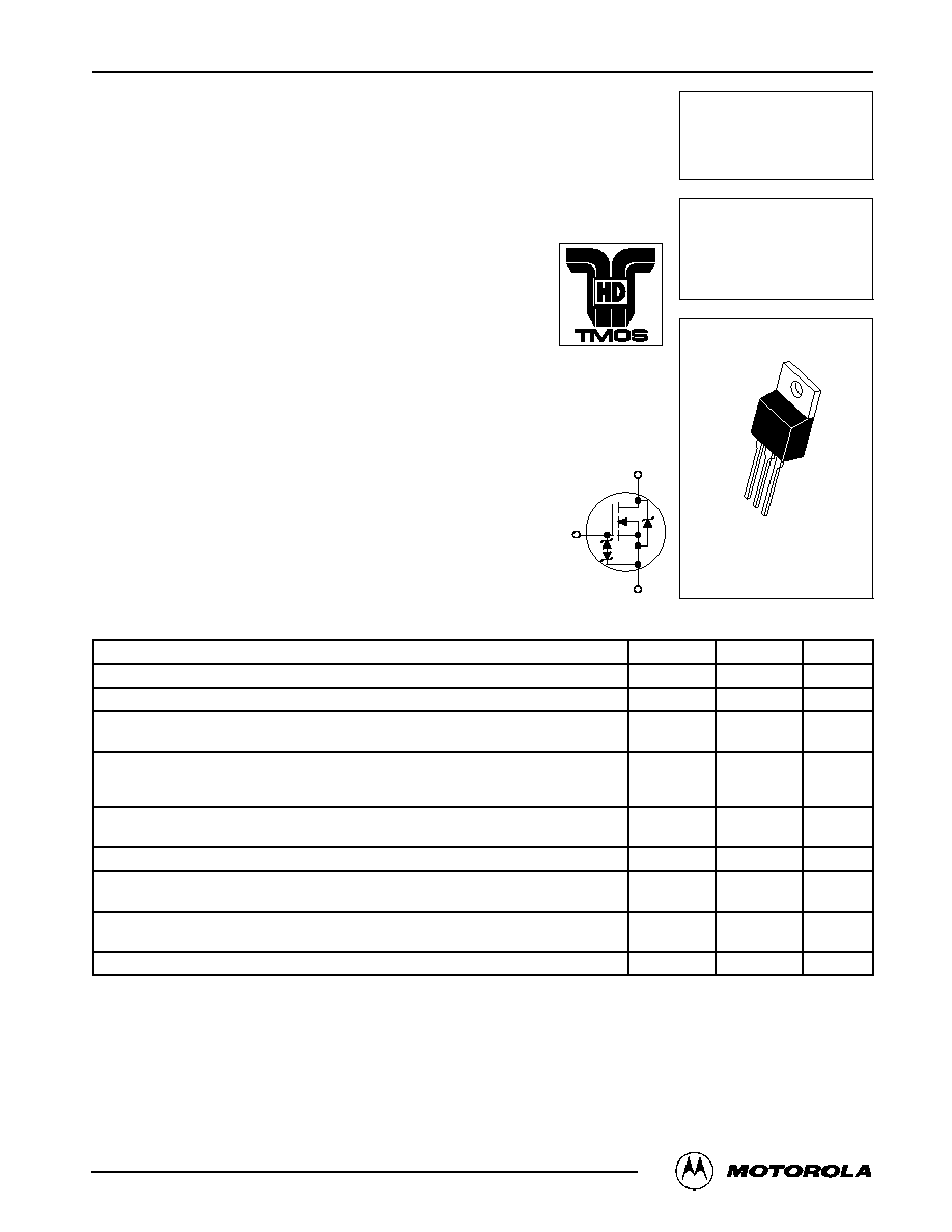
TMOS E-FET
.
TM
Power Field Effect Transistor
NChannel EnhancementMode Silicon Gate
This advanced high voltage TMOS EFET is designed to
withstand high energy in the avalanche mode and switch efficiently.
This new high energy device also offers a draintosource diode
with fast recovery time. Designed for high voltage, high speed
switching applications in power supplies, PWM motor controls and
other inductive loads, the avalanche energy capability is specified
to eliminate the guesswork in designs where inductive loads are
switched and offer additional safety margin against unexpected
voltage transients.
·
Avalanche Energy Capability Specified at Elevated
Temperature
·
SourcetoDrain Diode Recovery Time Comparable to a
Discrete Fast Recovery Diode
·
Low Stored Gate Charge for Efficient Switching
·
Internal SourcetoDrain Diode Designed to Replace External
Zener Transient SuppressorAbsorbs High Energy in the
Avalanche Mode
·
ESD Protected. Designed to Typically Withstand 400 V
Machine Model and 4000 V Human Body Model.
MAXIMUM RATINGS
(TJ = 25
°
C unless otherwise noted)
Rating
Symbol
Value
Unit
DraintoSource Voltage
VDSS
60
Vdc
DraintoGate Voltage (RGS = 1.0 M
)
VDGR
60
Vdc
GatetoSource Voltage -- Continuous
GatetoSource Voltage
-- NonRepetitive (tp
10 ms)
VGS
VGSM
±
20
±
40
Vdc
Vpk
Drain Current -- Continuous @ TC = 25
°
C
Drain Current
-- Continuous @ TC = 100
°
C
Drain Current
-- Single Pulse (tp
10
µ
s)
ID
ID
IDM
55
35.5
165
Adc
Apk
Total Power Dissipation @ TC = 25
°
C
Derate above 25
°
C
PD
113
0.91
Watts
W/
°
C
Operating and Storage Temperature Range
TJ, Tstg
55 to 150
°
C
Single Pulse DraintoSource Avalanche Energy -- Starting TJ = 25
°
C
(VDD = 25 Vdc, VDS = 60 Vdc, VGS = 10 Vdc, Peak IL = 55 Apk, L = 0.3 mH, RG = 25
)
EAS
454
mJ
Thermal Resistance -- JunctiontoCase
Thermal Resistance
-- JunctiontoAmbient
R
JC
R
JA
1.1
62.5
°
C/W
Maximum Lead Temperature for Soldering Purposes, 1/8
from case for 10 seconds
TL
260
°
C
This document contains information on a new product. Specifications and information herein are subject to change without notice.
EFET is a trademark of Motorola, Inc. TMOS is a registered trademark of Motorola, Inc.
Order this document
by MTP55N06Z/D
MOTOROLA
SEMICONDUCTOR TECHNICAL DATA
D
S
G
TM
MTP55N06Z
TMOS POWER FET
55 AMPERES
60 VOLTS
RDS(on) = 18 m
CASE 221A06, Style 5
TO220AB
©
Motorola, Inc. 1997
REV 1
MTP55N06Z
2
Motorola TMOS Power MOSFET Transistor Device Data
ELECTRICAL CHARACTERISTICS
(TC = 25
°
C unless otherwise noted)
Characteristic
Symbol
Min
Typ
Max
Unit
OFF CHARACTERISTICS
DraintoSource Breakdown Voltage
(Cpk
2.0)
(VGS = 0 Vdc, ID = 250
µ
Adc)
Temperature Coefficient (Positive)
V(BR)DSS
60
--
--
53
--
--
Vdc
mV/
°
C
Zero Gate Voltage Drain Current
(VDS = 60 Vdc, VGS = 0 Vdc)
(VDS = 60 Vdc, VGS = 0 Vdc, TJ = 125
°
C)
IDSS
--
--
--
--
1.0
10
µ
Adc
GateBody Leakage Current (VGS =
±
20 Vdc, VDS = 0 Vdc)
IGSS
--
--
100
nAdc
ON CHARACTERISTICS (1)
Gate Threshold Voltage
(Cpk
2.0)
(VDS = VGS, ID = 250
µ
Adc)
Threshold Temperature Coefficient (Negative)
VGS(th)
2.0
--
3.0
6.0
4.0
--
Vdc
mV/
°
C
Static DraintoSource OnResistance
(Cpk
2.0)
(VGS = 10 Vdc, ID = 27.5 Adc)
RDS(on)
--
14
16
m
DraintoSource OnVoltage (VGS = 10 Vdc)
(ID = 55 Adc)
(ID = 27.5 Adc, TJ = 125
°
C)
VDS(on)
--
--
0.825
0.74
1.2
1.0
Vdc
Forward Transconductance (VDS = 4.0 Vdc, ID = 27.5 Adc)
gFS
12
15
--
Mhos
DYNAMIC CHARACTERISTICS
Input Capacitance
(V
25 Vdc V
0 Vdc
Ciss
--
1390
1950
pF
Output Capacitance
(VDS = 25 Vdc, VGS = 0 Vdc,
f = 1.0 MHz)
Coss
--
520
730
Transfer Capacitance
f = 1.0 MHz)
Crss
--
119
238
SWITCHING CHARACTERISTICS (2)
TurnOn Delay Time
(V
30 Vd
I
55 Ad
td(on)
--
27
54
ns
Rise Time
(VDD = 30 Vdc, ID = 55 Adc,
VGS(on) = 10 Vdc
tr
--
157
314
TurnOff Delay Time
VGS(on) = 10 Vdc,
RG = 9.1
)
td(off)
--
116
232
Fall Time
G
)
tf
--
126
252
Gate Charge
(See Figure 8)
(V
48 Vd
I
55 Ad
QT
--
40
56
nC
(See Figure 8)
(VDS = 48 Vdc, ID = 55 Adc,
Q1
--
7.0
--
( DS
, D
,
VGS = 10 Vdc)
Q2
--
18
--
Q3
--
15
--
SOURCEDRAIN DIODE CHARACTERISTICS
Forward OnVoltage
(IS = 55 Adc, VGS = 0 Vdc)
(IS = 55 Adc, VGS = 0 Vdc, TJ = 125
°
C)
VSD
--
--
0.93
0.82
1.1
--
Vdc
Reverse Recovery Time
(I
55 Ad
V
0 Vd
trr
--
57
--
ns
(IS = 55 Adc, VGS = 0 Vdc,
ta
--
32
--
( S
,
GS
,
dIS/dt = 100 A/
µ
s)
tb
--
25
--
Reverse Recovery Stored Charge
QRR
--
0.11
--
µ
C
INTERNAL PACKAGE INDUCTANCE
Internal Drain Inductance
(Measured from contact screw on tab to center of die)
(Measured from drain lead 0.25
from package to center of die)
LD
--
--
3.5
4.5
--
--
nH
Internal Source Inductance
(Measured from the source lead 0.25
from package to source bond pad)
LS
--
7.5
--
(1) Pulse Test: Pulse Width
300
µ
s, Duty Cycle
2%.
(2) Switching characteristics are independent of operating junction temperature.
MTP55N06Z
3
Motorola TMOS Power MOSFET Transistor Device Data
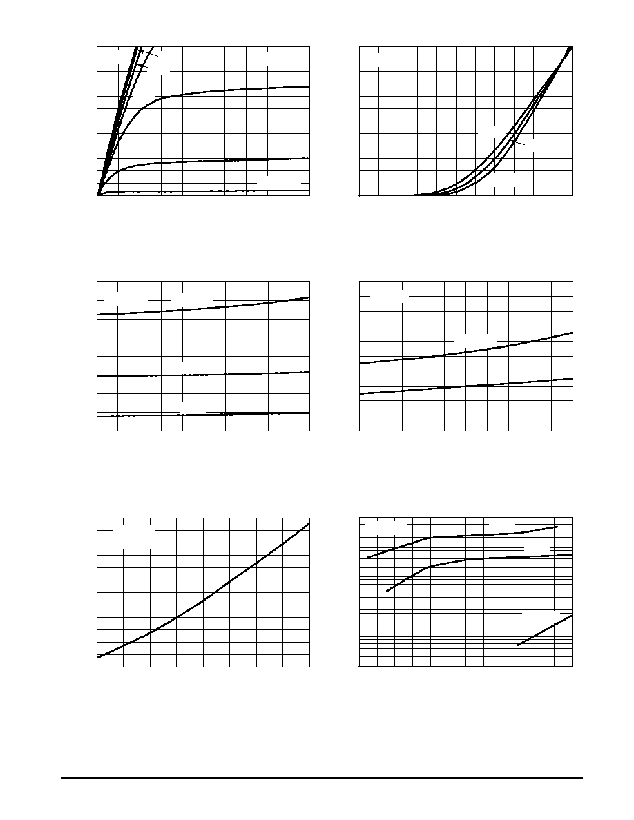
Figure 1. OnRegion Characteristics
Figure 2. Transfer Characteristics
Figure 3. OnResistance versus Drain Current
and Temperature
Figure 4. OnResistance versus Drain Current
and Gate Voltage
Figure 5. OnResistance Variation with
Temperature
Figure 6. DraintoSource Leakage Current
versus Voltage
3.0
4.5
0
VDS, DRAINTOSOURCE VOLTAGE (VOLTS)
60
40
20
50
10
VGS, GATETOSOURCE VOLTAGE (VOLTS)
4.4
6.4
2.0
40
20
10
0
60
10
ID, DRAIN CURRENT (AMPS)
24
20
16
12
8.0
ID, DRAIN CURRENT (AMPS)
20
10
15.0
14.6
14.2
13.8
13.4
13.0
30
25
25
50
TJ, JUNCTION TEMPERATURE (
°
C)
1.8
1.4
1.2
1.0
0.8
0.6
VDS, DRAINTOSOURCE VOLTAGE (VOLTS)
10
50
0
1000
100
10
1.0
0.1
0.01
0
I D
, DRAIN CURRENT
(AMPS)
I
R
0
1.5
0.5
1.0
2.0
2.5
3.5
4.0
4.8
5.2
2.4
2.8
3.2
3.6
4.0
30
50
60
20
30
40
50
40
50
60
, DRAINT
OSOURCE
RESIST
ANCE
(NORMALIZED)
R
DS(on)
50
150
75
1.6
20
60
30
40
I DSS
, LEAKAGE (nA)
5.0
30
5.6
6.0
, DRAIN CURRENT
(AMPS)
D
VDS
10 V
,
DRAINT
OSOURCE
RESIST
ANCE (m )
DS(on)
W
VGS = 10 V
R
,
DRAINT
OSOURCE
RESIST
ANCE (m )
DS(on)
W
100
125
VGS = 10 V
ID = 15 A
VGS = 0 V
VGS = 4.0 V
TJ = 25
°
C
5.0 V
6.0 V
10 V
9.0 V
8.0 V
7.0 V
TJ = 55
°
C
100
°
C
25
°
C
TJ = 100
°
C
55
°
C
25
°
C
VGS = 10 V
TJ = 25
°
C
15 V
TJ = 25
°
C
100
°
C
125
°
C
MTP55N06Z
4
Motorola TMOS Power MOSFET Transistor Device Data
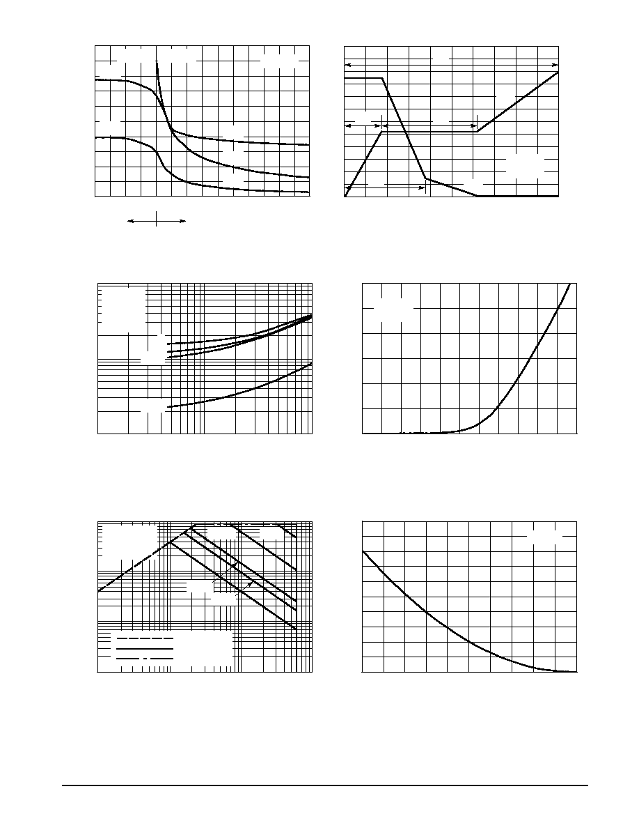
Figure 7. Capacitance Variation
Figure 8. GatetoSource and
DraintoSource Voltage versus Total Charge
Figure 9. Resistive Switching Time Variation
versus Gate Resistance
Figure 10. Diode Forward Voltage versus
Current
Figure 11. Maximum Rated Forward Biased
Safe Operating Area
Figure 12. Maximum Avalanche Energy versus
Starting Junction Temperature
10
25
10
GATETOSOURCE OR DRAINTOSOURCE VOLTAGE (VOLTS)
4000
3200
1600
2400
QG, TOTAL GATE CHARGE (nC)
24
40
0
8.0
4.0
2.0
0
100
1.0
RG, GATE RESISTANCE (OHMS)
1000
100
10
VSD, SOURCETODRAIN VOLTAGE (VOLTS)
0.54
0.5
30
20
10
0
0.58
1.0
10
0.1
VDS, DRAINTOSOURCE VOLTAGE (VOLTS)
100
10
1.0
0.1
TJ, STARTING JUNCTION TEMPERATURE (
°
C)
50
25
500
400
300
100
0
125
C, CAP
ACIT
ANCE
(pF)
V
t, TIME
(ns)
I S
, SOURCE CURRENT
(AMPS)
800
0
5.0
0
5.0
15
20
28
32
4.0
8.0
12
16
20
6.0
10
12
10
0.62 0.66 0.70 0.74
0.94
, DRAIN CURRENT
(AMPS)
I D
100
75
100
150
200
E
AS
, SINGLE PULSE DRAINT
OSOURCE
36
, GA
TET
OSOURCE
VOL
T
AGE
(VOL
TS)
GS
TJ = 25
°
C
ID = 30 A
VDD = 30 V
VGS = 10 V
0.78 0.82 0.86 0.90
TJ = 25
°
C
VGS = 0 V
A
V
ALANCHE ENERGY
(mJ)
ID = 30 A
TJ = 25
°
C
Ciss
Coss
Crss
Ciss
Crss
VDS = 0 V VGS = 0 V
VGS
VDS
32
16
8.0
0
24
40
48
V
,
DRAINT
OSOURCE
VOL
T
AGE
(VOL
TS)
DS
TJ = 25
°
C
ID = 30 A
VDS
VGS
QT
Q3
Q2
Q1
td(on)
VGS = 20 V
SINGLE PULSE
TC = 25
°
C
RDS(on) LIMIT
THERMAL LIMIT
PACKAGE LMIT
100
m
s
10
m
s
1.0 ms
10 ms
dc
td(off)
tr
tf
MTP55N06Z
5
Motorola TMOS Power MOSFET Transistor Device Data
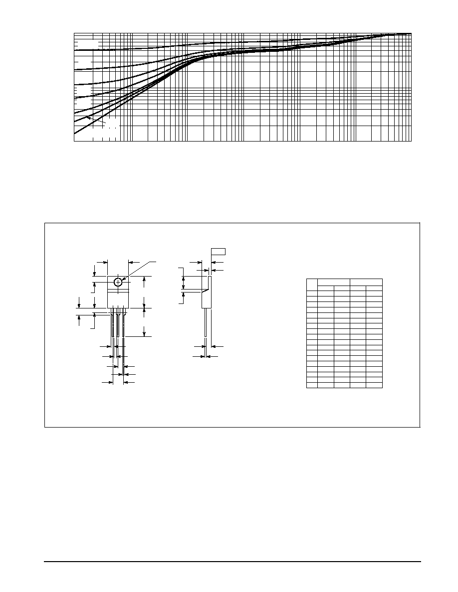
Figure 13. Thermal Response
0.001
0.01
0.00001
t, TIME (seconds)
1.0
0.1
r(t), EFFECTIVE
TRANSIENT
THERMAL
0.01
0.0001
RESIST
ANCE (NORMALIZED)
1.0
10
0.1
D = 0.5
0.2
0.1
0.05
0.02
SINGLE PULSE
0.01
PACKAGE DIMENSIONS
CASE 221A06
ISSUE Y
NOTES:
1. DIMENSIONING AND TOLERANCING PER ANSI
Y14.5M, 1982.
2. CONTROLLING DIMENSION: INCH.
3. DIMENSION Z DEFINES A ZONE WHERE ALL
BODY AND LEAD IRREGULARITIES ARE
ALLOWED.
STYLE 5:
PIN 1. GATE
2. DRAIN
3. SOURCE
4. DRAIN
DIM
MIN
MAX
MIN
MAX
MILLIMETERS
INCHES
A
0.570
0.620
14.48
15.75
B
0.380
0.405
9.66
10.28
C
0.160
0.190
4.07
4.82
D
0.025
0.035
0.64
0.88
F
0.142
0.147
3.61
3.73
G
0.095
0.105
2.42
2.66
H
0.110
0.155
2.80
3.93
J
0.018
0.025
0.46
0.64
K
0.500
0.562
12.70
14.27
L
0.045
0.060
1.15
1.52
N
0.190
0.210
4.83
5.33
Q
0.100
0.120
2.54
3.04
R
0.080
0.110
2.04
2.79
S
0.045
0.055
1.15
1.39
T
0.235
0.255
5.97
6.47
U
0.000
0.050
0.00
1.27
V
0.045
1.15
Z
0.080
2.04
B
Q
H
Z
L
V
G
N
A
K
F
1
2 3
4
D
SEATING
PLANE
T
C
S
T
U
R
J