 | ÐлекÑÑоннÑй компоненÑ: MTW20N50E | СкаÑаÑÑ:  PDF PDF  ZIP ZIP |
Äîêóìåíòàöèÿ è îïèñàíèÿ www.docs.chipfind.ru
1
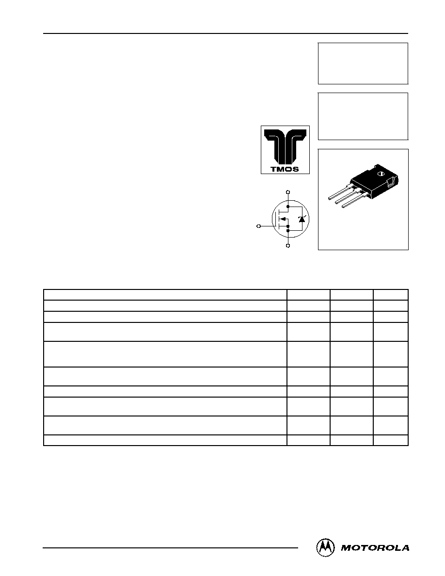
Motorola TMOS Power MOSFET Transistor Device Data
Designer's
TM
Data Sheet
TMOS E-FET
.
TM
Power Field Effect Transistor
TO-247 with Isolated Mounting Hole
NChannel EnhancementMode Silicon Gate
This high voltage MOSFET uses an advanced termination
scheme to provide enhanced voltageblocking capability without
degrading performance over time. In addition, this advanced TMOS
EFET is designed to withstand high energy in the avalanche and
commutation modes. The new energy efficient design also offers a
draintosource diode with a fast recovery time. Designed for high
voltage, high speed switching applications in power supplies,
converters and PWM motor controls, these devices are particularly
well suited for bridge circuits where diode speed and commutating
safe operating areas are critical and offer additional safety margin
against unexpected voltage transients.
·
Robust High Voltage Termination
·
Avalanche Energy Specified
·
SourcetoDrain Diode Recovery Time Comparable to a
Discrete Fast Recovery Diode
·
Diode is Characterized for Use in Bridge Circuits
·
IDSS and VDS(on) Specified at Elevated Temperature
·
Isolated Mounting Hole Reduces Mounting Hardware
MAXIMUM RATINGS
(TC = 25
°
C unless otherwise noted)
Rating
Symbol
Value
Unit
DrainSource Voltage
VDSS
500
Vdc
DrainGate Voltage (RGS = 1.0 M
)
VDGR
500
Vdc
GateSource Voltage -- Continuous
GateSource Voltage
-- NonRepetitive (tp
10 ms)
VGS
VGSM
±
20
±
40
Vdc
Vpk
Drain Current -- Continuous
Drain Current
-- Continuous @ 100
°
C
Drain Current
-- Single Pulse (tp
10
µ
s)
ID
ID
IDM
20
14.1
60
Adc
Apk
Total Power Dissipation
Derate above 25
°
C
PD
250
2.0
Watts
W/
°
C
Operating and Storage Temperature Range
TJ, Tstg
55 to 150
°
C
Single Pulse DraintoSource Avalanche Energy -- Starting TJ = 25
°
C
(VDD = 100 Vdc, VGS = 10 Vdc, IL = 20 Apk, L = 10 mH, RG = 25
)
EAS
2000
mJ
Thermal Resistance -- Junction to Case
Thermal Resistance
-- Junction to Ambient
R
JC
R
JA
0.50
40
°
C/W
Maximum Lead Temperature for Soldering Purposes, 1/8
from case for 10 seconds
TL
260
°
C
Designer's Data for "Worst Case" Conditions -- The Designer's Data Sheet permits the design of most circuits entirely from the information presented. SOA Limit
curves -- representing boundaries on device characteristics -- are given to facilitate "worst case" design.
EFET and Designer's are trademarks of Motorola, Inc. TMOS is a registered trademark of Motorola, Inc.
Preferred devices are Motorola recommended choices for future use and best overall value.
REV 4
Order this document
by MTW20N50E/D
MOTOROLA
SEMICONDUCTOR TECHNICAL DATA
MTW20N50E
TMOS POWER FET
20 AMPERES
500 VOLTS
RDS(on) = 0.24 OHM
Motorola Preferred Device
D
S
G
®
CASE 340K01, Style 1
TO247AE
©
Motorola, Inc. 1996

MTW20N50E
2
Motorola TMOS Power MOSFET Transistor Device Data
ELECTRICAL CHARACTERISTICS
(TJ = 25
°
C unless otherwise noted)
Characteristic
Symbol
Min
Typ
Max
Unit
OFF CHARACTERISTICS
DrainSource Breakdown Voltage
(VGS = 0 Vdc, ID = 250
µ
Adc)
Temperature Coefficient (Positive)
V(BR)DSS
500
--
--
583
--
--
Vdc
mV/
°
C
Zero Gate Voltage Drain Current
(VDS = 500 Vdc, VGS = 0 Vdc)
(VDS = 500 Vdc, VGS = 0 Vdc, TJ = 125
°
C)
IDSS
--
--
--
--
10
100
µ
Adc
GateBody Leakage Current (VGS =
±
20 Vdc, VDS = 0)
IGSS
--
--
100
nAdc
ON CHARACTERISTICS (1)
Gate Threshold Voltage
(VDS = VGS, ID = 250
µ
Adc)
Temperature Coefficient (Negative)
VGS(th)
2.0
--
3.0
7.0
4.0
--
Vdc
mV/
°
C
Static DrainSource OnResistance (VGS = 10 Vdc, ID = 10 Adc)
RDS(on)
--
0.20
0.24
Ohm
DrainSource OnVoltage (VGS = 10 Vdc)
(ID = 20 Adc)
(ID = 10 Adc, TJ = 125
°
C)
VDS(on)
--
--
5.75
--
6.0
6.0
Vdc
Forward Transconductance (VDS = 15 Vdc, ID = 10 Adc)
gFS
11
16.2
--
mhos
DYNAMIC CHARACTERISTICS
Input Capacitance
(V
25 Vdc V
0 Vdc
Ciss
--
3880
6950
pF
Output Capacitance
(VDS = 25 Vdc, VGS = 0 Vdc,
f = 1.0 MHz)
Coss
--
452
920
Reverse Transfer Capacitance
f = 1.0 MHz)
Crss
--
96
140
SWITCHING CHARACTERISTICS (2)
TurnOn Delay Time
(V
250 Vd
I
20 Ad
td(on)
--
29
55
ns
Rise Time
(VDD = 250 Vdc, ID = 20 Adc,
VGS = 10 Vdc
tr
--
90
165
TurnOff Delay Time
VGS = 10 Vdc,
RG = 9.1
)
td(off)
--
97
190
Fall Time
G
)
tf
--
84
170
Gate Charge
(See Figure 8)
(V
400 Vd
I
20 Ad
QT
--
100
132
nC
(VDS = 400 Vdc, ID = 20 Adc,
VGS = 10 Vdc)
Q1
--
20
--
VGS = 10 Vdc)
Q2
--
44
--
Q3
--
36
--
SOURCEDRAIN DIODE CHARACTERISTICS
Forward OnVoltage (1)
(IS = 20 Adc, VGS = 0 Vdc)
(IS = 20 Adc, VGS = 0 Vdc, TJ = 125
°
C)
VSD
--
--
0.916
0.81
1.1
--
Vdc
Reverse Recovery Time
(See Figure 14)
(I
20 Ad
V
0 Vd
trr
--
431
--
ns
(See Figure 14)
(IS = 20 Adc, VGS = 0 Vdc,
ta
--
272
--
( S
,
GS
,
dIS/dt = 100 A/
µ
s)
tb
--
159
--
Reverse Recovery Stored Charge
QRR
--
6.67
--
µ
C
INTERNAL PACKAGE INDUCTANCE
Internal Drain Inductance
(Measured from the drain lead 0.25
from package to center of die)
LD
--
5.0
--
nH
Internal Source Inductance
(Measured from the source lead 0.25
from package to source bond pad)
LS
--
13
--
nH
(1) Pulse Test: Pulse Width
300
µ
s, Duty Cycle
2%.
(2) Switching characteristics are independent of operating junction temperature.
MTW20N50E
3
Motorola TMOS Power MOSFET Transistor Device Data
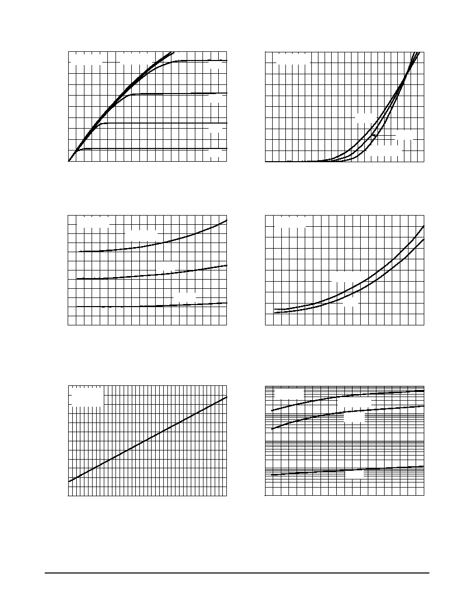
TYPICAL ELECTRICAL CHARACTERISTICS
R
DS(on)
, DRAINT
OSOURCE
RESIST
ANCE
(NORMALIZED)
R
DS(on)
, DRAINT
OSOURCE
RESIST
ANCE
(OHMS)
R
DS(on)
, DRAINT
OSOURCE
RESIST
ANCE
(OHMS)
0
4
8
12
16
20
0
16
24
32
40
VDS, DRAINTOSOURCE VOLTAGE (VOLTS)
Figure 1. OnRegion Characteristics
I D
, DRAIN CURRENT
(AMPS)
2.0
2.8
3.6
4.4
5.2
6.0
0
16
24
32
40
I D
, DRAIN CURRENT
(AMPS)
VGS, GATETOSOURCE VOLTAGE (VOLTS)
Figure 2. Transfer Characteristics
0
8
16
24
32
40
0
0.1
0.3
0.4
0.6
0
8
16
24
32
40
0.24
0.26
0.28
0.30
0.34
ID, DRAIN CURRENT (AMPS)
Figure 3. OnResistance versus Drain Current
and Temperature
ID, DRAIN CURRENT (AMPS)
Figure 4. OnResistance versus Drain Current
and Gate Voltage
50
0
0.8
1.6
2.4
0
100
200
300
400
500
1
10
100
1000
10000
TJ, JUNCTION TEMPERATURE (
°
C)
Figure 5. OnResistance Variation with
Temperature
VDS, DRAINTOSOURCE VOLTAGE (VOLTS)
Figure 6. DrainToSource Leakage
Current versus Voltage
I DSS
, LEAKAGE (nA)
25
0
25
50
75
100
125
150
TJ = 25
°
C
VDS
10 V
100
°
C
25
°
C
TJ = 55
°
C
TJ = 100
°
C
25
°
C
55
°
C
TJ = 25
°
C
VGS = 0 V
VGS = 10 V
VGS = 10 V
8 V
7 V
6 V
5 V
2
6
10
14
18
8
8
2.4
3.2
4.0
4.8
5.6
6.8
6.4
0.2
0.5
4
12
20
28
36
0.32
4
12
20
28
36
0.4
1.2
2.0
50
150
250
350
450
VGS = 10 V
15 V
100
°
C
25
°
C
TJ = 125
°
C
VGS = 10 V
ID = 10 A
9 V
MTW20N50E
4
Motorola TMOS Power MOSFET Transistor Device Data
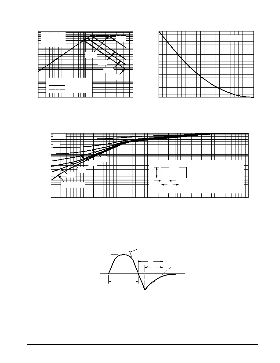
POWER MOSFET SWITCHING
Switching behavior is most easily modeled and predicted
by recognizing that the power MOSFET is charge controlled.
The lengths of various switching intervals (
t) are deter-
mined by how fast the FET input capacitance can be charged
by current from the generator.
The published capacitance data is difficult to use for calculat-
ing rise and fall because draingate capacitance varies
greatly with applied voltage. Accordingly, gate charge data is
used. In most cases, a satisfactory estimate of average input
current (IG(AV)) can be made from a rudimentary analysis of
the drive circuit so that
t = Q/IG(AV)
During the rise and fall time interval when switching a resis-
tive load, VGS remains virtually constant at a level known as
the plateau voltage, VSGP. Therefore, rise and fall times may
be approximated by the following:
tr = Q2 x RG/(VGG VGSP)
tf = Q2 x RG/VGSP
where
VGG = the gate drive voltage, which varies from zero to VGG
RG = the gate drive resistance
and Q2 and VGSP are read from the gate charge curve.
During the turnon and turnoff delay times, gate current is
not constant. The simplest calculation uses appropriate val-
ues from the capacitance curves in a standard equation for
voltage change in an RC network. The equations are:
td(on) = RG Ciss In [VGG/(VGG VGSP)]
td(off) = RG Ciss In (VGG/VGSP)
The capacitance (Ciss) is read from the capacitance curve at
a voltage corresponding to the offstate condition when cal-
culating td(on) and is read at a voltage corresponding to the
onstate when calculating td(off).
At high switching speeds, parasitic circuit elements com-
plicate the analysis. The inductance of the MOSFET source
lead, inside the package and in the circuit wiring which is
common to both the drain and gate current paths, produces a
voltage at the source which reduces the gate drive current.
The voltage is determined by Ldi/dt, but since di/dt is a func-
tion of drain current, the mathematical solution is complex.
The MOSFET output capacitance also complicates the
mathematics. And finally, MOSFETs have finite internal gate
resistance which effectively adds to the resistance of the
driving source, but the internal resistance is difficult to mea-
sure and, consequently, is not specified.
The resistive switching time variation versus gate resis-
tance (Figure 9) shows how typical switching performance is
affected by the parasitic circuit elements. If the parasitics
were not present, the slope of the curves would maintain a
value of unity regardless of the switching speed. The circuit
used to obtain the data is constructed to minimize common
inductance in the drain and gate circuit loops and is believed
readily achievable with board mounted components. Most
power electronic loads are inductive; the data in the figure is
taken with a resistive load, which approximates an optimally
snubbed inductive load. Power MOSFETs may be safely op-
erated into an inductive load; however, snubbing reduces
switching losses.
10
5
0
15
20
25
GATETOSOURCE OR DRAINTOSOURCE VOLTAGE (VOLTS)
C, CAP
ACIT
ANCE
(pF)
Figure 7a. Capacitance Variation
9000
8000
7000
4000
3000
2000
1000
0
VGS
VDS
TJ = 25
°
C
Figure 7b. High Voltage Capacitance
Variation
VDS, DRAINTOSOURCE VOLTAGE (VOLTS)
10
100
1000
10000
1000
100
10
C, CAP
ACIT
ANCE
(pF)
Ciss
Coss
Crss
VDS = 0 V
VGS = 0 V
TJ = 25
°
C
VGS = 0 V
6000
5000
5
10
Coss
Ciss
Ciss
Crss
Crss
MTW20N50E
5
Motorola TMOS Power MOSFET Transistor Device Data
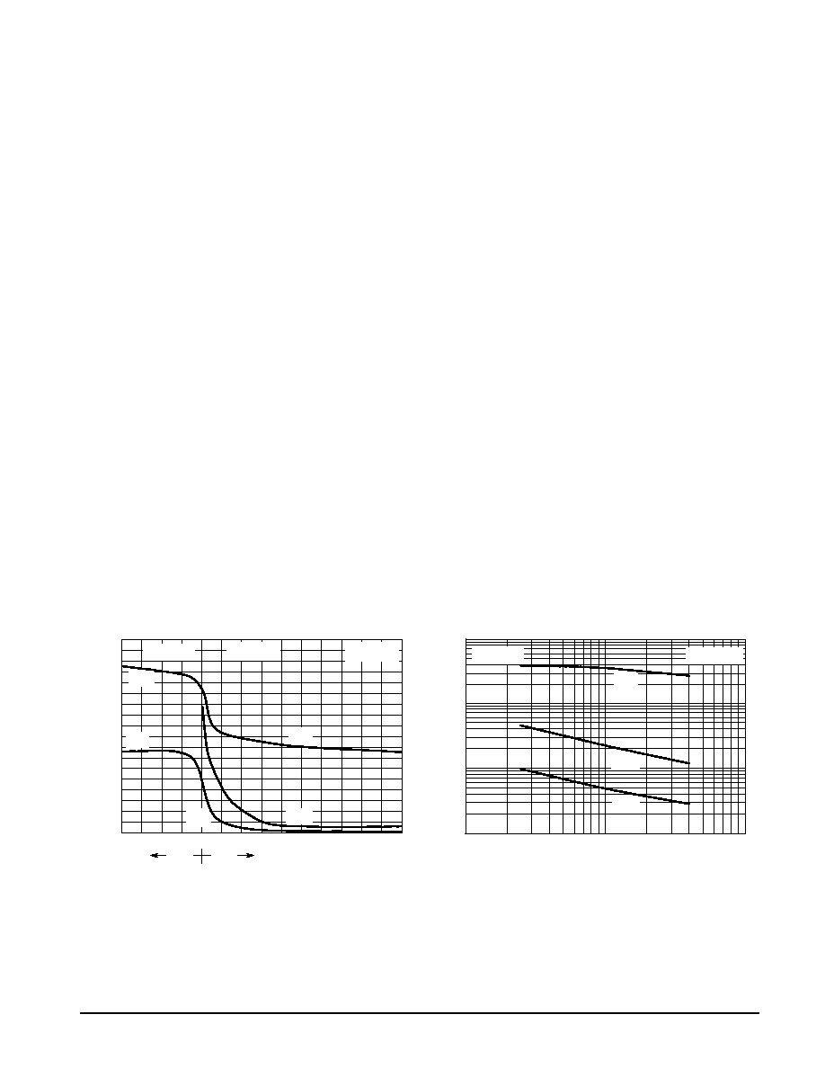
DRAINTOSOURCE DIODE CHARACTERISTICS
0.50 0.54 0.58 0.62 0.66
0.94
0
4
8
12
20
VSD, SOURCETODRAIN VOLTAGE (VOLTS)
Figure 10. Diode Forward Voltage versus Current
I S
, SOURCE CURRENT
(AMPS)
Figure 9. Resistive Switching Time
Variation versus Gate Resistance
RG, GATE RESISTANCE (OHMS)
1
10
100
1000
100
10
t, TIME
(ns)
VDD = 250 V
ID = 20 A
VGS = 10 V
TJ = 25
°
C
tr
tf
td(off)
td(on)
VGS = 0 V
TJ = 25
°
C
Figure 8. GateToSource and DrainToSource
Voltage versus Total Charge
500
V
GS
, GA
TET
OSOURCE
VOL
T
AGE
(VOL
TS)
400
300
200
100
0
0
8
6
0
QG, TOTAL GATE CHARGE (nC)
V
DS
, DRAINT
OSOURCE
VOL
T
AGE
(VOL
TS)
10
4
2
10
20
80
90
100
ID = 20 A
TJ = 25
°
C
VDS
30
40
50
60
70
0.74 0.78 0.82 0.86 0.90
0.70
Q3
Q1
Q2
QT
VGS
16
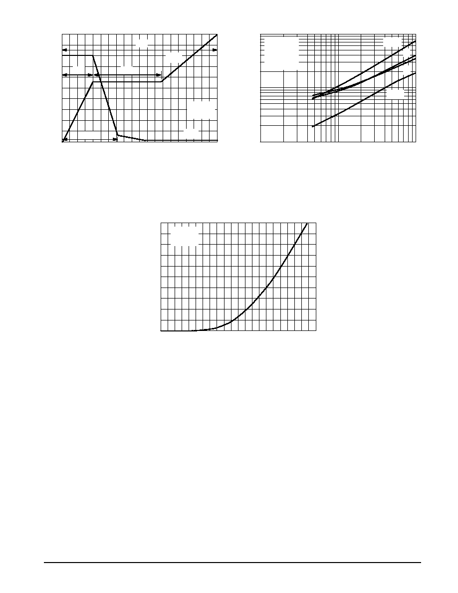
SAFE OPERATING AREA
The Forward Biased Safe Operating Area curves define
the maximum simultaneous draintosource voltage and
drain current that a transistor can handle safely when it is for-
ward biased. Curves are based upon maximum peak junc-
tion temperature and a case temperature (TC) of 25
°
C. Peak
repetitive pulsed power limits are determined by using the
thermal response data in conjunction with the procedures
discussed in AN569, "Transient Thermal ResistanceGeneral
Data and Its Use."
Switching between the offstate and the onstate may tra-
verse any load line provided neither rated peak current (IDM)
nor rated voltage (VDSS) is exceeded and the transition time
(tr,tf) do not exceed 10
µ
s. In addition the total power aver-
aged over a complete switching cycle must not exceed
(TJ(MAX) TC)/(R
JC).
A Power MOSFET designated EFET can be safely used
in switching circuits with unclamped inductive loads. For reli-
able operation, the stored energy from circuit inductance dis-
sipated in the transistor while in avalanche must be less than
the rated limit and adjusted for operating conditions differing
from those specified. Although industry practice is to rate in
terms of energy, avalanche energy capability is not a con-
stant. The energy rating decreases nonlinearly with an in-
crease of peak current in avalanche and peak junction
temperature.
Although many EFETs can withstand the stress of drain
tosource avalanche at currents up to rated pulsed current
(IDM), the energy rating is specified at rated continuous cur-
rent (ID), in accordance with industry custom. The energy rat-
ing must be derated for temperature as shown in the
accompanying graph (Figure 12). Maximum energy at cur-
rents below rated continuous ID can safely be assumed to
equal the values indicated.
MTW20N50E
6
Motorola TMOS Power MOSFET Transistor Device Data
SAFE OPERATING AREA
TJ, STARTING JUNCTION TEMPERATURE (
°
C)
E AS
, SINGLE PULSE DRAINT
OSOURCE
Figure 12. Maximum Avalanche Energy versus
Starting Junction Temperature
0.1
1.0
1000
VDS, DRAINTOSOURCE VOLTAGE (VOLTS)
Figure 11. Maximum Rated Forward Biased
Safe Operating Area
0.1
1.0
10
100
A
V
ALANCHE ENERGY
(mJ)
I D
, DRAIN CURRENT
(AMPS)
RDS(on) LIMIT
THERMAL LIMIT
PACKAGE LIMIT
0.01
0
25
50
75
100
125
10
2000
600
400
200
ID = 20 A
800
100
150
t, TIME (s)
Figure 13. Thermal Response
r(t)
, NORMALIZED EFFECTIVE
TRANSIENT
THERMAL
RESIST
ANCE
R
JC(t) = r(t) R
JC
D CURVES APPLY FOR POWER
PULSE TRAIN SHOWN
READ TIME AT t1
TJ(pk) TC = P(pk) R
JC(t)
P(pk)
t1
t2
DUTY CYCLE, D = t1/t2
Figure 14. Diode Reverse Recovery Waveform
di/dt
trr
ta
tp
IS
0.25 IS
TIME
IS
tb
100
µ
s
10
µ
s
1 ms
10 ms
dc
D = 0.5
0.2
0.1
0.05
0.02
0.01
SINGLE PULSE
1000
1600
1400
1200
1800
1.0E05
1.0E01
0.01
0.1
1.0
0.001
1.0E03
1.0E02
1.0E+01
1.0E+00
1.0E04
VGS = 20 V
SINGLE PULSE
TC = 25
°
C
MTW20N50E
7
Motorola TMOS Power MOSFET Transistor Device Data
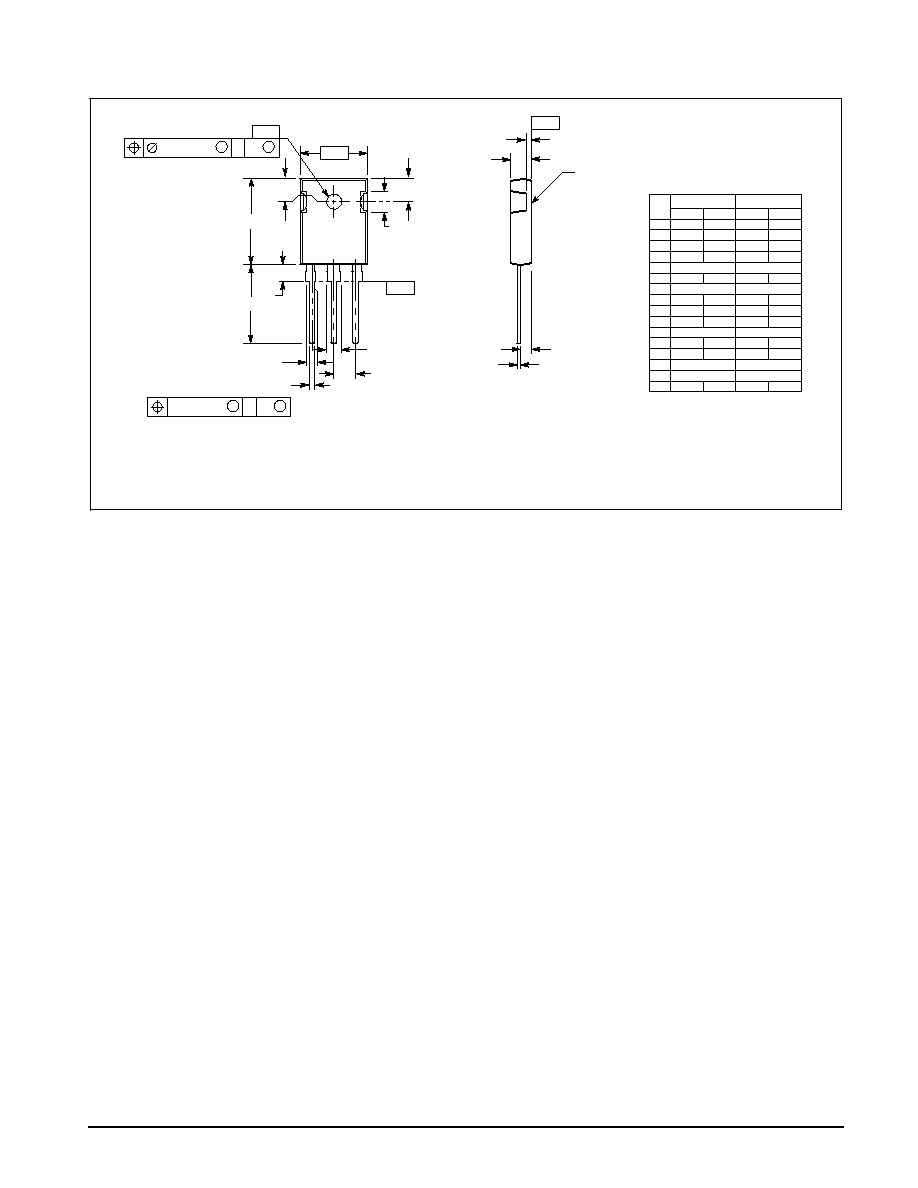
PACKAGE DIMENSIONS
CASE 340K01
ISSUE O
STYLE 1:
PIN 1. GATE
2. DRAIN
3. SOURCE
4. DRAIN
NOTES:
1.
DIMENSIONING AND TOLERANCING PER ANSI
Y14.5M, 1982.
2.
CONTROLLING DIMENSION: MILLIMETER.
R
P
A
K
V
F
D
G
U
L
E
0.25 (0.010)
M
T B
M
0.25 (0.010)
M
Y Q
S
J
H
C
4
1
2
3
T
B
Y
Q
DIM
MIN
MAX
MIN
MAX
INCHES
MILLIMETERS
A
19.7
20.3
0.776
0.799
B
15.3
15.9
0.602
0.626
C
4.7
5.3
0.185
0.209
D
1.0
1.4
0.039
0.055
E
1.27 REF
0.050 REF
F
2.0
2.4
0.079
0.094
G
5.5 BSC
0.216 BSC
H
2.2
2.6
0.087
0.102
J
0.4
0.8
0.016
0.031
K
14.2
14.8
0.559
0.583
L
5.5 NOM
0.217 NOM
P
3.7
4.3
0.146
0.169
Q
3.55
3.65
0.140
0.144
R
5.0 NOM
0.197 NOM
U
5.5 BSC
0.217 BSC
V
3.0
3.4
0.118
0.134

MTW20N50E
8
Motorola TMOS Power MOSFET Transistor Device Data
Motorola reserves the right to make changes without further notice to any products herein. Motorola makes no warranty, representation or guarantee regarding
the suitability of its products for any particular purpose, nor does Motorola assume any liability arising out of the application or use of any product or circuit, and
specifically disclaims any and all liability, including without limitation consequential or incidental damages. "Typical" parameters which may be provided in Motorola
data sheets and/or specifications can and do vary in different applications and actual performance may vary over time. All operating parameters, including "Typicals"
must be validated for each customer application by customer's technical experts. Motorola does not convey any license under its patent rights nor the rights of
others. Motorola products are not designed, intended, or authorized for use as components in systems intended for surgical implant into the body, or other
applications intended to support or sustain life, or for any other application in which the failure of the Motorola product could create a situation where personal injury
or death may occur. Should Buyer purchase or use Motorola products for any such unintended or unauthorized application, Buyer shall indemnify and hold Motorola
and its officers, employees, subsidiaries, affiliates, and distributors harmless against all claims, costs, damages, and expenses, and reasonable attorney fees
arising out of, directly or indirectly, any claim of personal injury or death associated with such unintended or unauthorized use, even if such claim alleges that
Motorola was negligent regarding the design or manufacture of the part. Motorola and are registered trademarks of Motorola, Inc. Motorola, Inc. is an Equal
Opportunity/Affirmative Action Employer.
How to reach us:
USA / EUROPE / Locations Not Listed: Motorola Literature Distribution;
JAPAN: Nippon Motorola Ltd.; TatsumiSPDJLDC, 6F SeibuButsuryuCenter,
P.O. Box 20912; Phoenix, Arizona 85036. 18004412447 or 6023035454
3142 Tatsumi KotoKu, Tokyo 135, Japan. 038135218315
MFAX: RMFAX0@email.sps.mot.com TOUCHTONE 6022446609
ASIA/PACIFIC: Motorola Semiconductors H.K. Ltd.; 8B Tai Ping Industrial Park,
INTERNET: http://DesignNET.com
51 Ting Kok Road, Tai Po, N.T., Hong Kong. 85226629298
MTW20N50E/D
*MTW20N50E/D*