
1
Motorola Small≠Signal Transistors, FETs and Diodes Device Data
Dual Bias Resistor Transistors
NPN Silicon Surface Mount Transistors with
Monolithic Bias Resistor Network
The BRT (Bias Resistor Transistor) contains a single transistor with a
monolithic bias network consisting of two resistors; a series base resistor and a
base≠emitter resistor. These digital transistors are designed to replace a single
device and its external resistor bias network. The BRT eliminates these
individual components by integrating them into a single device. In the
MUN5211DW1T1 series, two BRT devices are housed in the SOT≠363
package which is ideal for low power surface mount applications where board
space is at a premium.
∑
Simplifies Circuit Design
∑
Reduces Board Space
∑
Reduces Component Count
∑
Available in 8 mm, 7 inch/3000 Unit Tape and Reel.
MAXIMUM RATINGS
(TA = 25
∞
C unless otherwise noted, common for Q1 and Q2)
Rating
Symbol
Value
Unit
Collector-Base Voltage
VCBO
50
Vdc
Collector-Emitter Voltage
VCEO
50
Vdc
Collector Current
IC
100
mAdc
THERMAL CHARACTERISTICS
Thermal Resistance -- Junction-to-Ambient (surface mounted)
R
JA
833
∞
C/W
Operating and Storage Temperature Range
TJ, Tstg
≠ 65 to +150
∞
C
Total Package Dissipation @ TA = 25
∞
C(1)
PD
*
150
mW
DEVICE MARKING AND RESISTOR VALUES: MUN5211DW1T1 SERIES
Device
Marking
R1 (K)
R2 (K)
MUN5211DW1T1
MUN5212DW1T1
MUN5213DW1T1
MUN5214DW1T1
MUN5215DW1T1(2)
7A
7B
7C
7D
7E
10
22
47
10
10
10
22
47
47
MUN5216DW1T1(2)
MUN5230DW1T1(2)
MUN5231DW1T1(2)
MUN5232DW1T1(2)
MUN5233DW1T1(2)
MUN5234DW1T1(2)
MUN5235DW1T1(2)
7F
7G
7H
7J
7K
7L
7M
4.7
1.0
2.2
4.7
4.7
22
2.2
1.0
2.2
4.7
47
47
47
1. Device mounted on a FR-4 glass epoxy printed circuit board using the minimum recommended footprint.
2. New resistor combinations. Updated curves to follow in subsequent data sheets.
Thermal Clad is a trademark of the Bergquist Company
Preferred devices are Motorola recommended choices for future use and best overall value.
Order this document
by MUN5211DW1T1/D
MOTOROLA
SEMICONDUCTOR TECHNICAL DATA
Motorola Preferred Devices
MUN5211DW1T1
SERIES
CASE 419B≠01, STYLE 1
SOT≠363
Q1
R1
R2
R2
R1
Q2
(4)
(5)
(6)
(1)
(2)
(3)
1
2
3
6
5
4
©
Motorola, Inc. 1996
REV 1
MUN5211DW1T1 SERIES
2
Motorola Small≠Signal Transistors, FETs and Diodes Device Data
ELECTRICAL CHARACTERISTICS
(TA = 25
∞
C unless otherwise noted, common for Q1 and Q2)
Characteristic
Symbol
Min
Typ
Max
Unit
OFF CHARACTERISTICS
Collector-Base Cutoff Current (VCB = 50 V, IE = 0)
ICBO
--
--
100
nAdc
Collector-Emitter Cutoff Current (VCE = 50 V, IB = 0)
ICEO
--
--
500
nAdc
Emitter-Base Cutoff Current
MUN5211DW1T1
(VEB = 6.0 V, IC = 0)
MUN5212DW1T1
MUN5213DW1T1
MUN5214DW1T1
MUN5215DW1T1
MUN5216DW1T1
MUN5230DW1T1
MUN5231DW1T1
MUN5232DW1T1
MUN5233DW1T1
MUN5234DW1T1
MUN5235DW1T1
IEBO
--
--
--
--
--
--
--
--
--
--
--
--
--
--
--
--
--
--
--
--
--
--
--
--
0.5
0.2
0.1
0.2
0.9
1.9
4.3
2.3
1.5
0.18
0.13
0.2
mAdc
Collector-Base Breakdown Voltage (IC = 10
µ
A, IE = 0)
V(BR)CBO
50
--
--
Vdc
Collector-Emitter Breakdown Voltage(3) (IC = 2.0 mA, IB = 0)
V(BR)CEO
50
--
--
Vdc
ON CHARACTERISTICS(3)
DC Current Gain
MUN5211DW1T1
(VCE = 10 V, IC = 5.0 mA)
MUN5212DW1T1
MUN5213DW1T1
MUN5214DW1T1
MUN5215DW1T1
MUN5216DW1T1
MUN5230DW1T1
MUN5231DW1T1
MUN5232DW1T1
MUN5233DW1T1
MUN5234DW1T1
MUN5235DW1T1
hFE
35
60
80
80
160
160
3.0
8.0
15
80
80
80
60
100
140
140
350
350
5.0
15
30
200
150
140
--
--
--
--
--
--
--
--
--
--
--
--
Collector-Emitter Saturation Voltage (IC = 10 mA, IB = 0.3 mA)
(IC = 10 mA, IB = 5 mA) MUN5230DW1T1/MUN5231DW1T1
(IC = 10 mA, IB = 1 mA) MUN5215DW1T1/MUN5216DW1T1
MUN5232DW1T1/MUN5233DW1T1/MUN5234DW1T1
VCE(sat)
--
--
0.25
Vdc
Output Voltage (on)
(VCC = 5.0 V, VB = 2.5 V, RL = 1.0 k
)
MUN5211lDW1T1
MUN5212DW1T1
MUN5214DW1T1
MUN5215DW1T1
MUN5216DW1T1
MUN5230DW1T1
MUN5231DW1T1
MUN5232DW1T1
MUN5233DW1T1
MUN5234DW1T1
MUN5235DW1T1
(VCC = 5.0 V, VB = 3.5 V, RL = 1.0 k
)
MUN5213DW1T1
VOL
--
--
--
--
--
--
--
--
--
--
--
--
--
--
--
--
--
--
--
--
--
--
--
--
0.2
0.2
0.2
0.2
0.2
0.2
0.2
0.2
0.2
0.2
0.2
0.2
Vdc
3. Pulse Test: Pulse Width < 300
µ
s, Duty Cycle < 2.0%
MUN5211DW1T1 SERIES
3
Motorola Small≠Signal Transistors, FETs and Diodes Device Data
ELECTRICAL CHARACTERISTICS
(TA = 25
∞
C unless otherwise noted, common for Q1 and Q2)
(Continued)
Characteristic
Symbol
Min
Typ
Max
Unit
Output Voltage (off) (VCC = 5.0 V, VB = 0.5 V, RL = 1.0 k
)
(VCC = 5.0 V, VB = 0.050 V, RL = 1.0 k
)
MUN5230DW1T1
(VCC = 5.0 V, VB = 0.25 V, RL = 1.0 k
)
MUN5215DW1T1
MUN5216DW1T1
MUN5233DW1T1
VOH
4.9
--
--
Vdc
Input Resistor
MUN5211DW1T1
MUN5212DW1T1
MUN5213DW1T1
MUN5214DW1T1
MUN5215DW1T1
MUN5216DW1T1
MUN5230DW1T1
MUN5231DW1T1
MUN5232DW1T1
MUN5233DW1T1
MUN5234DW1T1
MUN5235DW1T1
R1
7.0
15.4
32.9
7.0
7.0
3.3
0.7
1.5
3.3
3.3
15.4
1.54
10
22
47
10
10
4.7
1.0
2.2
4.7
4.7
22
2.2
13
28.6
61.1
13
13
6.1
1.3
2.9
6.1
6.1
28.6
2.86
k
Resistor Ratio MUN5211DW1T1/MUN5212DW1T1/MUN5213DW1T1
MUN5214DW1T1
MUN5215DW1T1/MUN5216DW1T1
MUN5230DW1T1/MUN5231DW1T1/MUN5232DW1T1
MUN5233DW1T1
MUN5234DW1T1
MUN5235DW1T1
R1/R2
0.8
0.17
--
0.8
0.055
0.38
0.038
1.0
0.21
--
1.0
0.1
0.47
0.047
1.2
0.25
--
1.2
0.185
0.56
0.056
Figure 1. Derating Curve
250
200
150
100
50
0
≠ 50
0
50
100
150
TA, AMBIENT TEMPERATURE (
∞
C)
P
D
, POWER DISSIP
A
TION
(MILLIW
A
TTS)
R
JA = 833
∞
C/W
MUN5211DW1T1 SERIES
4
Motorola Small≠Signal Transistors, FETs and Diodes Device Data
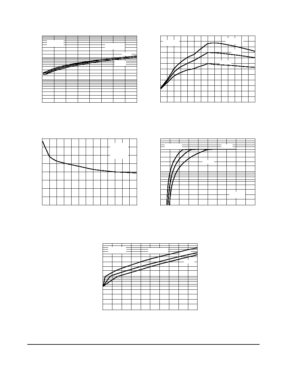
TYPICAL ELECTRICAL CHARACTERISTICS -- MUN5211DW1T1
V
in
, INPUT
VOL
T
AGE (VOL
TS)
I C
, COLLECT
OR
CURRENT
(mA)
h
FE
, DC CURRENT
GAIN (NORMALIZED)
Figure 2. VCE(sat) versus IC
10
0
20
30
IC, COLLECTOR CURRENT (mA)
10
1
0.1
TA = ≠25
∞
C
75
∞
C
25
∞
C
40
50
Figure 3. DC Current Gain
Figure 4. Output Capacitance
1
0.1
0.01
0.001
0
20
40
50
IC, COLLECTOR CURRENT (mA)
V
CE(sat)
, MAXIMUM COLLECT
OR
VOL
T
AGE (VOL
TS)
1000
100
10
1
10
100
IC, COLLECTOR CURRENT (mA)
TA = 75
∞
C
25
∞
C
≠25
∞
C
TA = ≠25
∞
C
25
∞
C
Figure 5. Output Current versus Input Voltage
75
∞
C
25
∞
C
TA = ≠25
∞
C
100
10
1
0.1
0.01
0.001
0
1
2
3
4
Vin, INPUT VOLTAGE (VOLTS)
5
6
7
8
9
10
Figure 6. Input Voltage versus Output Current
50
0
10
20
30
40
4
3
1
2
0
VR, REVERSE BIAS VOLTAGE (VOLTS)
C
ob
, CAP
ACIT
ANCE
(pF)
75
∞
C
VCE = 10 V
f = 1 MHz
IE = 0 V
TA = 25
∞
C
VO = 5 V
VO = 0.2 V
IC/IB = 10

MUN5211DW1T1 SERIES
5
Motorola Small≠Signal Transistors, FETs and Diodes Device Data
TYPICAL ELECTRICAL CHARACTERISTICS -- MUN5212DW1T1
V
in
, INPUT
VOL
T
AGE (VOL
TS)
I C
, COLLECT
OR
CURRENT
(mA)
h
FE
, DC CURRENT
GAIN (NORMALIZED)
Figure 7. VCE(sat) versus IC
Figure 8. DC Current Gain
Figure 9. Output Capacitance
Figure 10. Output Current versus Input Voltage
1000
10
IC, COLLECTOR CURRENT (mA)
TA = 75
∞
C
25
∞
C
≠25
∞
C
100
10
1
100
75
∞
C
25
∞
C
100
0
Vin, INPUT VOLTAGE (VOLTS)
10
1
0.1
0.01
0.001
2
4
6
8
10
TA = ≠25
∞
C
0
IC, COLLECTOR CURRENT (mA)
100
TA = ≠25
∞
C
75
∞
C
10
1
0.1
10
20
30
40
50
25
∞
C
Figure 11. Input Voltage versus Output Current
0.001
V
CE(sat)
, MAXIMUM COLLECT
OR
VOL
T
AGE (VOL
TS)
TA = ≠25
∞
C
75
∞
C
25
∞
C
0.01
0.1
1
40
IC, COLLECTOR CURRENT (mA)
0
20
50
50
0
10
20
30
40
4
3
2
1
0
VR, REVERSE BIAS VOLTAGE (VOLTS)
C
ob
, CAP
ACIT
ANCE
(pF)
IC/IB = 10
VCE = 10 V
f = 1 MHz
IE = 0 V
TA = 25
∞
C
VO = 5 V
VO = 0.2 V
MUN5211DW1T1 SERIES
6
Motorola Small≠Signal Transistors, FETs and Diodes Device Data
TYPICAL ELECTRICAL CHARACTERISTICS -- MUN5213DW1T1
V
in
, INPUT
VOL
T
AGE (VOL
TS)
I C
, COLLECT
OR
CURRENT
(mA)
h
FE
, DC CURRENT
GAIN (NORMALIZED)
Figure 12. VCE(sat) versus IC
0
2
4
6
8
10
100
10
1
0.1
0.01
0.001
Vin, INPUT VOLTAGE (VOLTS)
TA = ≠25
∞
C
75
∞
C
25
∞
C
Figure 13. DC Current Gain
Figure 14. Output Capacitance
100
10
1
0.1
0
10
20
30
40
50
IC, COLLECTOR CURRENT (mA)
Figure 15. Output Current versus Input Voltage
1000
10
IC, COLLECTOR CURRENT (mA)
TA = 75
∞
C
25
∞
C
≠25
∞
C
100
10
1
100
25
∞
C
75
∞
C
50
0
10
20
30
40
1
0.8
0.6
0.4
0.2
0
VR, REVERSE BIAS VOLTAGE (VOLTS)
C
ob
, CAP
ACIT
ANCE
(pF)
Figure 16. Input Voltage versus Output Current
0
20
40
50
10
1
0.1
0.01
IC, COLLECTOR CURRENT (mA)
25
∞
C
75
∞
C
V
CE(sat)
, MAXIMUM COLLECT
OR
VOL
T
AGE (VOL
TS)
VCE = 10 V
f = 1 MHz
IE = 0 V
TA = 25
∞
C
VO = 5 V
VO = 0.2 V
IC/IB = 10
TA = ≠25
∞
C
TA = ≠25
∞
C
MUN5211DW1T1 SERIES
7
Motorola Small≠Signal Transistors, FETs and Diodes Device Data
TYPICAL ELECTRICAL CHARACTERISTICS -- MUN5214DW1T1
10
1
0.1
0
10
20
30
40
50
100
10
1
0
2
4
6
8
10
4
3.5
3
2.5
2
1.5
1
0.5
0
0
2
4
6
8
10
15
20
25 30
35
40
45
50
VR, REVERSE BIAS VOLTAGE (VOLTS)
V
in
, INPUT
VOL
T
AGE (VOL
TS)
I C
, COLLECT
OR
CURRENT
(mA)
h
FE
, DC CURRENT
GAIN (NORMALIZED)
Figure 17. VCE(sat) versus IC
IC, COLLECTOR CURRENT (mA)
0
20
40
60
80
V
CE(sat)
, MAXIMUM COLLECT
OR
VOL
T
AGE (VOL
TS)
Figure 18. DC Current Gain
1
10
100
IC, COLLECTOR CURRENT (mA)
Figure 19. Output Capacitance
Figure 20. Output Current versus Input Voltage
Vin, INPUT VOLTAGE (VOLTS)
C
ob
, CAP
ACIT
ANCE
(pF)
Figure 21. Input Voltage versus Output Current
IC, COLLECTOR CURRENT (mA)
1
0.1
0.01
0.001
≠25
∞
C
25
∞
C
TA = 75
∞
C
VCE = 10
300
250
200
150
100
50
0
2
4
6
8
15
20 40
50 60 70 80
90
f = 1 MHz
lE = 0 V
TA = 25
∞
C
25
∞
C
IC/IB = 10
TA = ≠25
∞
C
TA = 75
∞
C
25
∞
C
≠25
∞
C
VO = 0.2 V
TA = ≠25
∞
C
75
∞
C
VO = 5 V
25
∞
C
75
∞
C
MUN5211DW1T1 SERIES
8
Motorola Small≠Signal Transistors, FETs and Diodes Device Data
INFORMATION FOR USING THE SOT≠363 SURFACE MOUNT PACKAGE
MINIMUM RECOMMENDED FOOTPRINTS FOR SURFACE MOUNTED APPLICATIONS
Surface mount board layout is a critical portion of the total
design. The footprint for the semiconductor packages must
be the correct size to insure proper solder connection
interface between the board and the package. With the
correct pad geometry, the packages will self align when
subjected to a solder reflow process.
SOT≠363
……
……
……
……
……
……
……
……
……
……
……
……
……
……
0.5 mm (min)
0.4 mm (min)
0.65 mm
0.65 mm
1.9 mm
SOT≠363 POWER DISSIPATION
The power dissipation of the SOT≠363 is a function of the
pad size. This can vary from the minimum pad size for
soldering to the pad size given for maximum power
dissipation. Power dissipation for a surface mount device is
determined by TJ(max), the maximum rated junction tempera-
ture of the die, R
JA, the thermal resistance from the device
junction to ambient; and the operating temperature, TA.
Using the values provided on the data sheet, PD can be
calculated as follows:
PD =
TJ(max) ≠ TA
R
JA
The values for the equation are found in the maximum
ratings table on the data sheet. Substituting these values into
the equation for an ambient temperature TA of 25
∞
C, one can
calculate the power dissipation of the device which in this
case is 150 milliwatts.
PD =
150
∞
C ≠ 25
∞
C
833
∞
C/W
= 150 milliwatts
The 833
∞
C/W for the SOT≠363 package assumes the use
of the recommended footprint on a glass epoxy printed circuit
board to achieve a power dissipation of 150 milliwatts. There
are other alternatives to achieving higher power dissipation
from the SOT≠363 package. Another alternative would be to
use a ceramic substrate or an aluminum core board such as
Thermal Clad
TM
. Using a board material such as Thermal
Clad, an aluminum core board, the power dissipation can be
doubled using the same footprint.
SOLDERING PRECAUTIONS
The melting temperature of solder is higher than the rated
temperature of the device. When the entire device is heated
to a high temperature, failure to complete soldering within a
short time could result in device failure. Therefore, the
following items should always be observed in order to
minimize the thermal stress to which the devices are
subjected.
∑
Always preheat the device.
∑
The delta temperature between the preheat and
soldering should be 100
∞
C or less.*
∑
When preheating and soldering, the temperature of the
leads and the case must not exceed the maximum
temperature ratings as shown on the data sheet. When
using infrared heating with the reflow soldering method,
the difference should be a maximum of 10
∞
C.
∑
The soldering temperature and time should not exceed
260
∞
C for more than 10 seconds.
∑
When shifting from preheating to soldering, the
maximum temperature gradient should be 5
∞
C or less.
∑
After soldering has been completed, the device should
be allowed to cool naturally for at least three minutes.
Gradual cooling should be used as the use of forced
cooling will increase the temperature gradient and result
in latent failure due to mechanical stress.
∑
Mechanical stress or shock should not be applied during
cooling.
* Soldering a device without preheating can cause excessive
thermal shock and stress which can result in damage to the
device.
MUN5211DW1T1 SERIES
9
Motorola Small≠Signal Transistors, FETs and Diodes Device Data
SOLDER STENCIL GUIDELINES
Prior to placing surface mount components onto a printed
circuit board, solder paste must be applied to the pads. A
solder stencil is required to screen the optimum amount of
solder paste onto the footprint. The stencil is made of brass
or stainless steel with a typical thickness of 0.008 inches.
The stencil opening size for the surface mounted package
should be the same as the pad size on the printed circuit
board, i.e., a 1:1 registration.
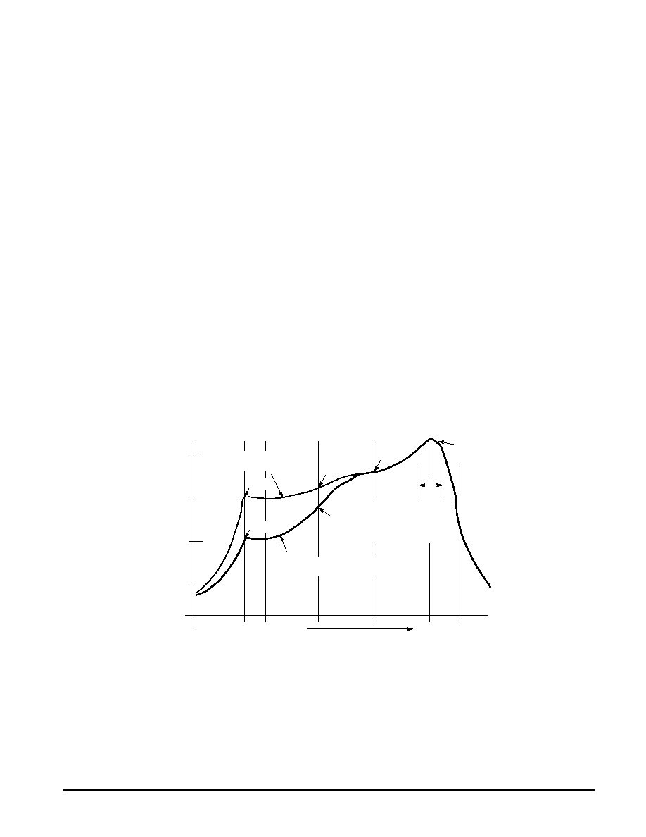
TYPICAL SOLDER HEATING PROFILE
For any given circuit board, there will be a group of control
settings that will give the desired heat pattern. The operator
must set temperatures for several heating zones, and a
figure for belt speed. Taken together, these control settings
make up a heating "profile" for that particular circuit board.
On machines controlled by a computer, the computer
remembers these profiles from one operating session to the
next. Figure 25 shows a typical heating profile for use when
soldering a surface mount device to a printed circuit board.
This profile will vary among soldering systems but it is a good
starting point. Factors that can affect the profile include the
type of soldering system in use, density and types of
components on the board, type of solder used, and the type
of board or substrate material being used. This profile shows
temperature versus time. The line on the graph shows the
actual temperature that might be experienced on the surface
of a test board at or near a central solder joint. The two
profiles are based on a high density and a low density board.
The Vitronics SMD310 convection/infrared reflow soldering
system was used to generate this profile. The type of solder
used was 62/36/2 Tin Lead Silver with a melting point
between 177 ≠189
∞
C. When this type of furnace is used for
solder reflow work, the circuit boards and solder joints tend to
heat first. The components on the board are then heated by
conduction. The circuit board, because it has a large surface
area, absorbs the thermal energy more efficiently, then
distributes this energy to the components. Because of this
effect, the main body of a component may be up to 30
degrees cooler than the adjacent solder joints.
STEP 1
PREHEAT
ZONE 1
"RAMP"
STEP 2
VENT
"SOAK"
STEP 3
HEATING
ZONES 2 & 5
"RAMP"
STEP 4
HEATING
ZONES 3 & 6
"SOAK"
STEP 5
HEATING
ZONES 4 & 7
"SPIKE"
STEP 6
VENT
STEP 7
COOLING
200
∞
C
150
∞
C
100
∞
C
50
∞
C
TIME (3 TO 7 MINUTES TOTAL)
TMAX
SOLDER IS LIQUID FOR
40 TO 80 SECONDS
(DEPENDING ON
MASS OF ASSEMBLY)
205
∞
TO 219
∞
C
PEAK AT
SOLDER JOINT
DESIRED CURVE FOR LOW
MASS ASSEMBLIES
100
∞
C
150
∞
C
160
∞
C
140
∞
C
Figure 22. Typical Solder Heating Profile
DESIRED CURVE FOR HIGH
MASS ASSEMBLIES
170
∞
C

MUN5211DW1T1 SERIES
10
Motorola Small≠Signal Transistors, FETs and Diodes Device Data
PACKAGE DIMENSIONS
CASE 419B≠01
ISSUE C
NOTES:
1. DIMENSIONING AND TOLERANCING PER ANSI
Y14.5M, 1982.
2. CONTROLLING DIMENSION: INCH.
DIM
A
MIN
MAX
MIN
MAX
MILLIMETERS
1.80
2.20
0.071
0.087
INCHES
B
1.15
1.35
0.045
0.053
C
0.80
1.10
0.031
0.043
D
0.10
0.30
0.004
0.012
G
0.65 BSC
0.026 BSC
H
≠≠≠
0.10
≠≠≠
0.004
J
0.10
0.25
0.004
0.010
K
0.10
0.30
0.004
0.012
N
0.20 REF
0.008 REF
S
2.00
2.20
0.079
0.087
V
0.30
0.40
0.012
0.016
B
0.2 (0.008)
M
M
1
2
3
A
G
V
S
H
C
N
J
K
6
5
4
≠B≠
D
6 PL
STYLE 1:
PIN 1. EMITTER 2
2. BASE 2
3. COLLECTOR 1
4. EMITTER 1
5. BASE 1
6. COLLECTOR 2
Motorola reserves the right to make changes without further notice to any products herein. Motorola makes no warranty, representation or guarantee regarding
the suitability of its products for any particular purpose, nor does Motorola assume any liability arising out of the application or use of any product or circuit, and
specifically disclaims any and all liability, including without limitation consequential or incidental damages. "Typical" parameters which may be provided in Motorola
data sheets and/or specifications can and do vary in different applications and actual performance may vary over time. All operating parameters, including "Typicals"
must be validated for each customer application by customer's technical experts. Motorola does not convey any license under its patent rights nor the rights of
others. Motorola products are not designed, intended, or authorized for use as components in systems intended for surgical implant into the body, or other
applications intended to support or sustain life, or for any other application in which the failure of the Motorola product could create a situation where personal injury
or death may occur. Should Buyer purchase or use Motorola products for any such unintended or unauthorized application, Buyer shall indemnify and hold Motorola
and its officers, employees, subsidiaries, affiliates, and distributors harmless against all claims, costs, damages, and expenses, and reasonable attorney fees
arising out of, directly or indirectly, any claim of personal injury or death associated with such unintended or unauthorized use, even if such claim alleges that
Motorola was negligent regarding the design or manufacture of the part. Motorola and are registered trademarks of Motorola, Inc. Motorola, Inc. is an Equal
Opportunity/Affirmative Action Employer.
Mfax is a trademark of Motorola, Inc.
How to reach us:
USA / EUROPE / Locations Not Listed: Motorola Literature Distribution;
JAPAN: Nippon Motorola Ltd.; Tatsumi≠SPD≠JLDC, 6F Seibu≠Butsuryu≠Center,
P.O. Box 5405, Denver, Colorado 80217. 303≠675≠2140 or 1≠800≠441≠2447
3≠14≠2 Tatsumi Koto≠Ku, Tokyo 135, Japan. 81≠3≠3521≠8315
Mfax
TM
: RMFAX0@email.sps.mot.com ≠ TOUCHTONE 602≠244≠6609
ASIA/PACIFIC: Motorola Semiconductors H.K. Ltd.; 8B Tai Ping Industrial Park,
INTERNET: http://Design≠NET.com
51 Ting Kok Road, Tai Po, N.T., Hong Kong. 852≠26629298
MUN5211DW1T1/D