 | Электронный компонент: MUR190E | Скачать:  PDF PDF  ZIP ZIP |

1
Rectifier Device Data
SWITCHMODE
TM
Power Rectifiers
Ultrafast "E'' Series with High Reverse
Energy Capability
. . . designed for use in switching power supplies, inverters and as
free wheeling diodes, these state¡of¡the¡art devices have the
following features:
╖
20 mjoules Avalanche Energy Guaranteed
╖
Excellent Protection Against Voltage Transients in Switching
Inductive Load Circuits
╖
Ultrafast 75 Nanosecond Recovery Time
╖
175
░
C Operating Junction Temperature
╖
Low Forward Voltage
╖
Low Leakage Current
╖
High Temperature Glass Passivated Junction
╖
Reverse Voltage to 1000 Volts
Mechanical Characteristics:
╖
Case: Epoxy, Molded
╖
Weight: 0.4 gram (approximately)
╖
Finish: All External Surfaces Corrosion Resistant and Terminal
Leads are Readily Solderable
╖
Lead and Mounting Surface Temperature for Soldering
Purposes: 220
░
C Max. for 10 Seconds, 1/16
from case
╖
Shipped in plastic bags, 1000 per bag
╖
Available Tape and Reeled, 5000 per reel, by adding a "RL''
suffix to the part number
╖
Polarity: Cathode Indicated by Polarity Band
╖
Marking: U190E, U1100E
MAXIMUM RATINGS
R i
S
b l
MUR
U i
Rating
Symbol
190E
1100E
Unit
Peak Repetitive Reverse Voltage
Working Peak Reverse Voltage
DC Blocking Voltage
VRRM
VRWM
VR
900
1000
Volts
Average Rectified Forward Current (Square Wave)
(Mounting Method #3 Per Note 1)
IF(AV)
1.0 @ TA = 95
░
C
Amps
Nonrepetitive Peak Surge Current
(Surge applied at rated load conditions, halfwave, single phase, 60 Hz)
IFSM
35
Amps
Operating Junction Temperature and Storage Temperature
TJ, Tstg
*
65 to +175
░
C
THERMAL CHARACTERISTICS
Maximum Thermal Resistance, Junction to Ambient
R
JA
See Note 1
░
C/W
(1) Pulse Test: Pulse Width = 300
╡
s, Duty Cycle
2.0%.
SWITCHMODE is a trademark of Motorola, Inc.
Preferred devices are Motorola recommended choices for future use and best overall value.
⌐
Motorola, Inc. 1996
Order this document
by MUR190E/D
MOTOROLA
SEMICONDUCTOR TECHNICAL DATA
MUR190E
MUR1100E
ULTRAFAST
RECTIFIERS
1.0 AMPERE
900¡1000 VOLTS
CASE 59¡04
MUR1100E is a
Motorola Preferred Device
Rev 1

MUR190E MUR1100E
2
Rectifier Device Data
ELECTRICAL CHARACTERISTICS
R i
S
b l
MUR
U i
Rating
Symbol
190E
1100E
Unit
Maximum Instantaneous Forward Voltage (1)
(iF = 1.0 Amp, TJ = 150
░
C)
(iF = 1.0 Amp, TJ = 25
░
C)
vF
1.50
1.75
Volts
Maximum Instantaneous Reverse Current (1)
(Rated dc Voltage, TJ = 100
░
C)
(Rated dc Voltage, TJ = 25
░
C)
iR
600
10
╡
A
Maximum Reverse Recovery Time
(IF = 1.0 Amp, di/dt = 50 Amp/
╡
s)
(IF = 0.5 Amp, iR = 1.0 Amp, IREC = 0.25 Amp)
trr
100
75
ns
Maximum Forward Recovery Time
(IF = 1.0 Amp, di/dt = 100 Amp/
╡
s, Recovery to 1.0 V)
tfr
75
ns
Controlled Avalanche Energy (See Test Circuit in Figure 6)
WAVAL
10
mJ
(1) Pulse Test: Pulse Width = 300
╡
s, Duty Cycle
2.0%.

MUR190E MUR1100E
3
Rectifier Device Data
ELECTRICAL CHARACTERISTICS
Figure 1. Typical Forward Voltage
vF, INSTANTANEOUS VOLTAGE (VOLTS)
0.3
0.9
0.5
1.3
3.0
0.01
0.03
0.02
0.2
0.1
20
2.0
0.7
0.3
0.05
0.5
5.0
, INST
ANT
ANEOUS
FOR
W
ARD
CURRENT
(AMPS)
F
2.3
VR, REVERSE VOLTAGE (VOLTS)
0
300
200
500
600
1000
0.1
0.01
10
100
TJ = 175
░
C
I R
100
400
1000
Figure 2. Typical Reverse Current*
IF(AV), AVERAGE FORWARD CURRENT (AMPS)
0
1.0
2.0
3.0
4.0
5.0
P
F(A
V)
0
0.5
1.0
1.5
2.0
2.5
TA, AMBIENT TEMPERATURE (
░
C)
0
50
0
2.0
1.0
3.0
5.0
4.0
I
250
Figure 3. Current Derating
(Mounting Method #3 Per Note 1)
Figure 4. Power Dissipation
0
3.0
10
20
2.0
10
20
VR, REVERSE VOLTAGE (VOLTS)
Figure 5. Typical Capacitance
0.7
0.07
1.0
7.0
1.7
2.1
100
░
C
TJ = 175
░
C
25
░
C
800
900
700
1.0
,
REVERSE
CURRENT
(
A)
100
░
C
25
░
C
150
100
200
* The curves shown are typical for the highest voltage device in the
grouping. Typical reverse current for lower voltage selections can be
estimated from these same curves if VR is sufficiently below rated VR.
C, CAP
ACIT
ANCE
(pF)
,
A
VERAGE POWER DISSIP
A
TION
(W
A
TTS)
TJ = 25
░
C
i
, A
VERAGE
FOR
W
ARD
CURRENT
(AMPS)
F(A
V)
30
40
50
7.0
5.0
TJ = 175
░
C
RATED VR
R
q
JA = 50
░
C/W
dc
SQUARE WAVE
m
(CAPACITIVE LOAD)
I
PK
I
AV
+
20
SQUARE WAVE
dc
5.0
10
1.1
1.5
1.9
10
MUR190E MUR1100E
4
Rectifier Device Data
MERCURY
SWITCH
VD
ID
DUT
40 mH COIL
+VDD
IL
S1
BVDUT
IL
ID
VDD
t0
t1
t2
t
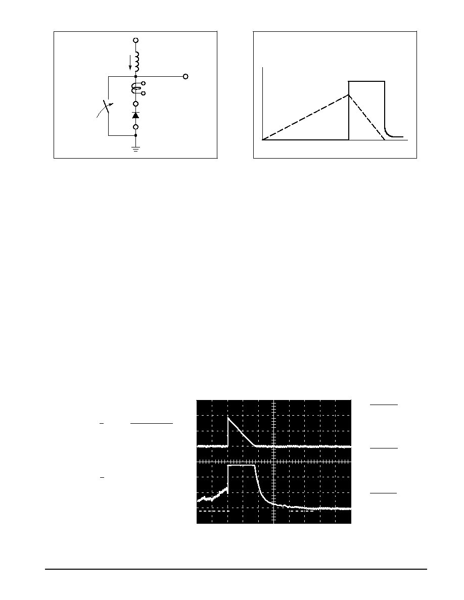
Figure 6. Test Circuit
Figure 7. Current¡Voltage Waveforms
The unclamped inductive switching circuit shown in
Figure 6 was used to demonstrate the controlled avalanche
capability of the new "E'' series Ultrafast rectifiers. A mercury
switch was used instead of an electronic switch to simulate a
noisy environment when the switch was being opened.
When S1 is closed at t0 the current in the inductor IL ramps
up linearly; and energy is stored in the coil. At t1 the switch is
opened and the voltage across the diode under test begins to
rise rapidly, due to di/dt effects, when this induced voltage
reaches the breakdown voltage of the diode, it is clamped at
BVDUT and the diode begins to conduct the full load current
which now starts to decay linearly through the diode, and
goes to zero at t2.
By solving the loop equation at the point in time when S1 is
opened; and calculating the energy that is transferred to the
diode it can be shown that the total energy transferred is
equal to the energy stored in the inductor plus a finite amount
of energy from the VDD power supply while the diode is in
breakdown (from t1 to t2) minus any losses due to finite com-
ponent resistances. Assuming the component resistive ele-
ments are small Equation (1) approximates the total energy
transferred to the diode. It can be seen from this equation
that if the VDD voltage is low compared to the breakdown
voltage of the device, the amount of energy contributed by
the supply during breakdown is small and the total energy
can be assumed to be nearly equal to the energy stored in
the coil during the time when S1 was closed, Equation (2).
The oscilloscope picture in Figure 8, shows the information
obtained for the MUR8100E (similar die construction as the
MUR1100E Series) in this test circuit conducting a peak cur-
rent of one ampere at a breakdown voltage of 1300 volts,
and using Equation (2) the energy absorbed by the
MUR8100E is approximately 20 mjoules.
Although it is not recommended to design for this condi-
tion, the new "E'' series provides added protection against
those unforeseen transient viruses that can produce unex-
plained random failures in unfriendly environments.
W
AVAL
[
1
2
LI
2
LPK
BV
DUT
BV
DUT
¡V
DD
W
AVAL
[
1
2
LI
2
LPK
Figure 8. Current¡Voltage Waveforms
CHANNEL 2:
IL
0.5 AMPS/DIV.
CHANNEL 1:
VDUT
500 VOLTS/DIV.
TIME BASE:
20
m
s/DIV.
EQUATION (1):
EQUATION (2):
CH1
CH2
REF
REF
CH1
CH2
ACQUISITIONS
SAVEREF SOURCE
1
217:33 HRS
STACK
A
20
m
s
953 V
VERT
500V
50mV

MUR190E MUR1100E
5
Rectifier Device Data
Lead Length, L
Mounting
Method
1/8
1/4
1/2
Units
1
2
3
52
67
R
JA
65
72
80
87
50
░
C/W
░
C/W
░
C/W
TYPICAL VALUES FOR R
JA IN STILL AIR
Data shown for thermal resistance junction to
ambient (R
JA) for the mountings shown is to be used
as typical guideline values for preliminary
engineering or in case the tie point temperature
cannot be measured.
NOTE 1 -- AMBIENT MOUNTING DATA
MOUNTING METHOD 1
MOUNTING METHOD 2
MOUNTING METHOD 3
╔╔╔╔╔╔╔╔╔╔╔
╔╔╔╔╔╔╔╔╔╔╔
L
L
╔╔╔╔╔╔╔╔╔╔╔╔
╔╔╔╔╔╔╔╔╔╔╔╔
L
L
Vector Pin Mounting
╔╔
╔╔
╔╔
╔╔
╔╔
╔╔
╔╔
╔╔
L = 3/8
Board Ground Plane
P.C. Board with
1¡1/2 X 1¡1/2 Copper Surface

MUR190E MUR1100E
6
Rectifier Device Data
PACKAGE DIMENSIONS
CASE 59¡04
ISSUE M
K
A
D
K
B
DIM
MIN
MAX
MIN
MAX
INCHES
MILLIMETERS
A
5.97
6.60
0.235
0.260
B
2.79
3.05
0.110
0.120
D
0.76
0.86
0.030
0.034
K
27.94
¡¡¡
1.100
¡¡¡
NOTES:
1. ALL RULES AND NOTES ASSOCIATED WITH
JEDEC DO¡41 OUTLINE SHALL APPLY.
2. POLARITY DENOTED BY CATHODE BAND.
3. LEAD DIAMETER NOT CONTROLLED WITHIN F
DIMENSION.
Motorola reserves the right to make changes without further notice to any products herein. Motorola makes no warranty, representation or guarantee regarding
the suitability of its products for any particular purpose, nor does Motorola assume any liability arising out of the application or use of any product or circuit, and
specifically disclaims any and all liability, including without limitation consequential or incidental damages. "Typical" parameters which may be provided in Motorola
data sheets and/or specifications can and do vary in different applications and actual performance may vary over time. All operating parameters, including "Typicals"
must be validated for each customer application by customer's technical experts. Motorola does not convey any license under its patent rights nor the rights of
others. Motorola products are not designed, intended, or authorized for use as components in systems intended for surgical implant into the body, or other
applications intended to support or sustain life, or for any other application in which the failure of the Motorola product could create a situation where personal injury
or death may occur. Should Buyer purchase or use Motorola products for any such unintended or unauthorized application, Buyer shall indemnify and hold Motorola
and its officers, employees, subsidiaries, affiliates, and distributors harmless against all claims, costs, damages, and expenses, and reasonable attorney fees
arising out of, directly or indirectly, any claim of personal injury or death associated with such unintended or unauthorized use, even if such claim alleges that
Motorola was negligent regarding the design or manufacture of the part. Motorola and are registered trademarks of Motorola, Inc. Motorola, Inc. is an Equal
Opportunity/Affirmative Action Employer.
Mfax is a trademark of Motorola, Inc.
How to reach us:
USA / EUROPE / Locations Not Listed: Motorola Literature Distribution;
JAPAN: Nippon Motorola Ltd.: SPD, Strategic Planning Office, 4¡32¡1,
P.O. Box 5405, Denver, Colorado 80217. 1¡303¡675¡2140 or 1¡800¡441¡2447
Nishi¡Gotanda, Shinagawa¡ku, Tokyo 141, Japan. 81¡3¡5487¡8488
Customer Focus Center: 1¡800¡521¡6274
Mfax
TM
: RMFAX0@email.sps.mot.com ¡ TOUCHTONE 1¡602¡244¡6609
ASIA/PACIFIC: Motorola Semiconductors H.K. Ltd.; 8B Tai Ping Industrial Park,
Motorola Fax Back System
¡ US & Canada ONLY 1¡800¡774¡1848
51 Ting Kok Road, Tai Po, N.T., Hong Kong. 852¡26629298
¡ http://sps.motorola.com/mfax/
HOME PAGE: http://motorola.com/sps/
MUR190E/D