 | Электронный компонент: MUR3020 | Скачать:  PDF PDF  ZIP ZIP |
1
Rectifier Device Data
SWITCHMODE
TM
Power Rectifiers
. . . designed for use in switching power supplies, inverters and as free
wheeling diodes, these state¡of¡the¡art devices have the following features:
╖
Ultrafast 35 and 60 Nanosecond Recovery Time
╖
175
░
C Operating Junction Temperature
╖
High Voltage Capability to 600 Volts
╖
Low Forward Drop
╖
Low Leakage Specified @ 150
░
C Case Temperature
╖
Current Derating Specified @ Both Case and Ambient Temperatures
╖
Epoxy Meets UL94, VO @ 1/8
╖
High Temperature Glass Passivated Junction
Mechanical Characteristics:
╖
Case: Epoxy, Molded
╖
Weight: 4.3 grams (approximately)
╖
Finish: All External Surfaces Corrosion Resistant and
Terminal Leads are Readily Solderable
╖
Lead Temperature for Soldering Purposes: 260
░
C Max.
for 10 Seconds
╖
Shipped 30 units per plastic tube
╖
Marking: U3020, U3040, U3060
MAXIMUM RATINGS, PER LEG
Rating
Symbol
MUR3020PT
MUR3040PT
MUR3060PT
Unit
Peak Repetitive Reverse Voltage
Working Peak Reverse Voltage
DC Blocking Voltage
VRRM
VRWM
VR
200
400
600
Volts
Average Rectified Forward Current (Rated VR)
Per Leg
Per Device
IF(AV)
15 @ TC = 150
░
C
30 @ TC = 150
░
C
15 @ TC =
30 145
░
C
Amps
Peak Rectified Forward Current, Per Leg
(Rated VR, Square Wave, 20 kHz, TC = 150
░
C)
IFRM
30
@ TC = 150
░
C
30
@ TC =145
░
C
Amps
Nonrepetitive Peak Surge Current
(Surge applied at rated load conditions,
halfwave, single phase, 60 Hz) Per Leg
IFSM
200
150
Amps
Operating Junction and Storage Temperature
TJ, Tstg
¡ 65 to +175
░
C
THERMAL CHARACTERISTICS PER DIODE LEG
Maximum Thermal Resistance -- Junction to Case
-- Junction to Ambient
R
JC
R
JA
1.5
40
░
C/W
ELECTRICAL CHARACTERISTICS PER DIODE LEG
Maximum Instantaneous Forward Voltage (1)
(IF = 15 Amp, TC = 150
░
C)
(IF = 15 Amp, TC = 25
░
C)
VF
0.85
1.05
1.12
1.25
1.2
1.5
Volts
Maximum Instantaneous Reverse Current (1)
(Rated DC Voltage, TJ = 150
░
C)
(Rated DC Voltage, TJ = 25
░
C)
iR
500
10
1000
10
╡
A
Maximum Reverse Recovery Time
(iF = 1.0 Amp, di/dt = 50 Amps/
╡
s)
trr
35
60
ns
(1) Pulse Test: Pulse Width = 300
╡
s, Duty Cycle
2.0%.
SWITCHMODE is a trademark of Motorola, Inc.
Preferred devices are Motorola recommended choices for future use and best overall value.
Order this document
by MUR3020PT/D
MOTOROLA
SEMICONDUCTOR TECHNICAL DATA
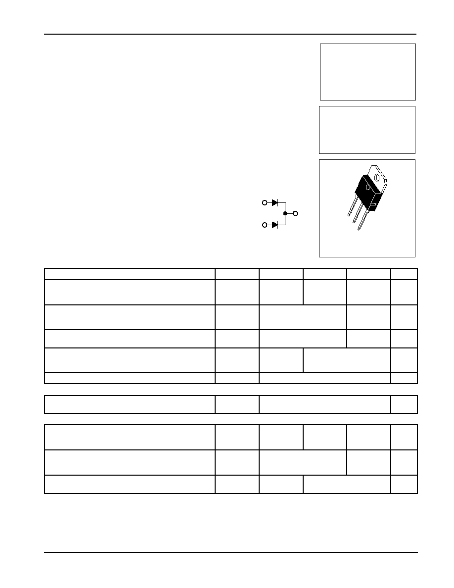
1
3
2, 4
ULTRAFAST RECTIFIERS
30 AMPERES
200¡400¡600 VOLTS
CASE 340D¡02, Style 2
TO¡218AC
MUR3020PT
MUR3040PT
MUR3060PT
1
2
3
*
*
*Motorola Preferred Devices
Rev 4
MUR3020PT MUR3040PT MUR3060PT
2
Rectifier Device Data
100
0.1
0.2
0.3
0.5
1
2
3
5
10
20
30
50
i F
, INST
ANT
ANEOUS
FOR
W
ARD
CURRENT
(AMPS)
0.2
0.4
0.6
0.8
1
1.2
1.4
1.6
vF, INSTANTANEOUS VOLTAGE (VOLTS)
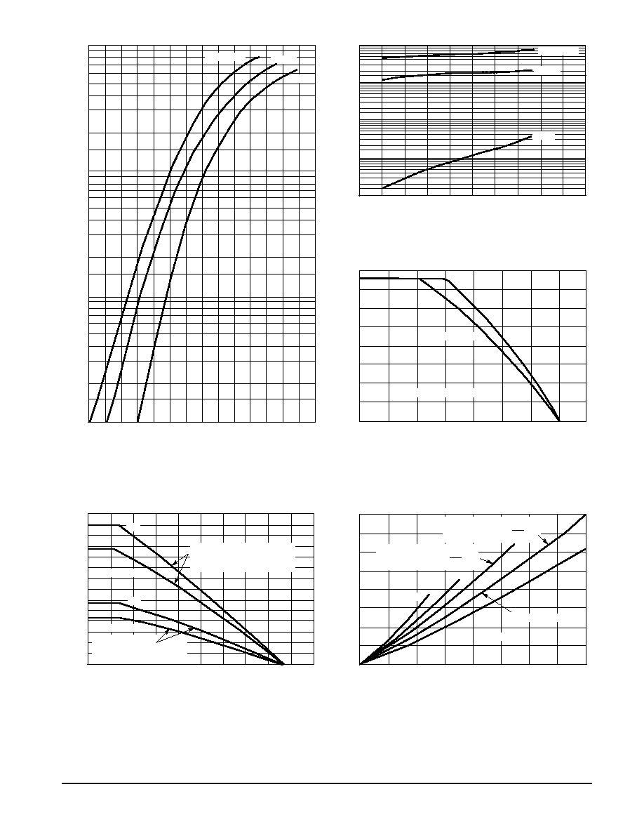
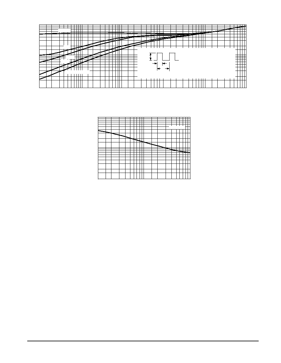
Figure 1. Typical Forward Voltage (Per Leg)
TJ = 150
░
C
100
░
C
25
░
C
100
0.01
0.02
0.05
0.1
0.2
0.5
1
2
5
10
20
50
0
20
40
60
80
100
120
140
160
180
200
I R
, REVERSE CURRENT
(
A
)
╡
VR, REVERSE VOLTAGE (VOLTS)
Figure 2. Typical Reverse Current (Per Leg)
TJ = 150
░
C
100
░
C
25
░
C
16
14
12
10
8
6
4
2
0
140
150
160
170
180
I F(A
V)
, A
VERAGE
FOR
W
ARD
CURRENT
(AMPS)
TC, CASE TEMPERATURE (
░
C)
Figure 3. Current Derating, Case (Per Leg)
SQUARE WAVE
RATED VOLTAGE APPLIED
dc
14
12
10
8
6
4
2
0
0
20
40
60
80
100
120
140
160
180
200
TA, AMBIENT TEMPERATURE (
░
C)
Figure 4. Current Derating, Ambient (Per Leg)
P
F(A
V)
,
A
VERAGE POWER DISSIP
A
TION
(W
A
TTS)
16
14
12
10
8
6
4
2
0
0
IF(AV), AVERAGE FORWARD CURRENT (AMPS)
Figure 5. Power Dissipation (Per Leg)
2
4
6
8
10
12
14
16
R
JA = 15
░
C/W AS OBTAINED
USING A SMALL FINNED
HEAT SINK.
dc
SQUARE WAVE
dc
R
JA = 40
░
C/W
AS OBTAINED IN FREE AIR
WITH NO HEAT SINK.
SQUARE WAVE
TJ = 125
░
C
SQUARE WAVE
20
10
dc
(RESISTIVE LOAD)
IPK
IAV
=
(CAPACITIVE LOAD)
IPK
IAV
= 5
I F(A
V)
, A
VERAGE
FOR
W
ARD
CURRENT
(AMPS)
MUR3020PT MUR3040PT MUR3060PT
3
Rectifier Device Data
100
0.1
0.2
0.3
0.5
1
2
3
5
10
20
30
50
i F
, INST
ANT
ANEOUS
FOR
W
ARD
CURRENT
(AMPS)
0.2
0.4
0.6
0.8
1
1.2
1.4
1.6
vF, INSTANTANEOUS VOLTAGE (VOLTS)
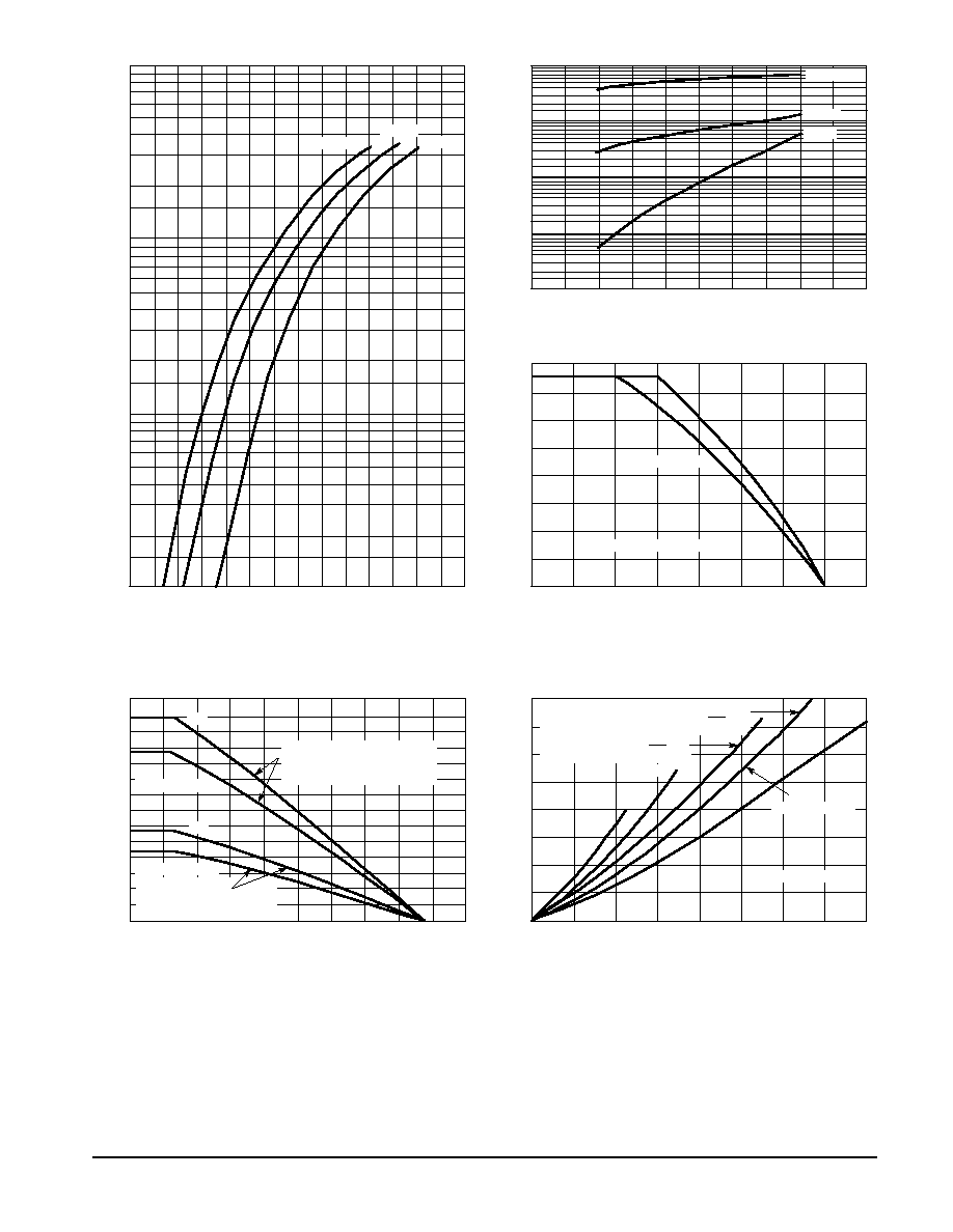
Figure 6. Typical Forward Voltage (Per Leg)
100
0.01
0.02
0.05
0.1
0.2
0.5
1
2
5
10
20
50
0
50
100
150
200
250
300
350
400
450
500
I R
, REVERSE CURRENT
(
A
)
╡
VR, REVERSE VOLTAGE (VOLTS)
Figure 7. Typical Reverse Current (Per Leg)
16
14
12
10
8
6
4
2
0
140
150
160
170
180
I F(A
V)
, A
VERAGE
FOR
W
ARD
CURRENT
(AMPS)
TC, CASE TEMPERATURE (
░
C)
Figure 8. Current Derating, Case (Per Leg)
dc
14
12
10
8
6
4
2
0
0
120
140
160
180
200
TA, AMBIENT TEMPERATURE (
░
C)
Figure 9. Current Derating, Ambient (Per Leg)
P
F(A
V)
,
A
VERAGE POWER DISSIP
A
TION
(W
A
TTS)
16
14
12
10
8
6
4
2
0
0
IF(AV), AVERAGE FORWARD CURRENT (AMPS)
Figure 10. Power Dissipation (Per Leg)
2
4
6
8
10
12
14
16
20
dc
I F(A
V)
, A
VERAGE
FOR
W
ARD
CURRENT
(AMPS)
TJ = 150
░
C
100
░
C
25
░
C
TJ = 150
░
C
100
░
C
25
░
C
SQUARE WAVE
RATED VOLTAGE APPLIED
R
JA = 15
░
C/W AS OBTAINED
USING A SMALL FINNED
HEAT SINK.
SQUARE WAVE
dc
dc
R
JA = 40
░
C/W
AS OBTAINED IN FREE AIR
WITH NO HEAT SINK.
SQUARE WAVE
20
40
60
80
100
(RESISTIVE¡INDUCTIVE LOAD)
IPK
IAV
=
TJ = 125
░
C
SQUARE WAVE
10
(CAPACITIVE LOAD)
IPK
IAV
= 5
MUR3020PT MUR3040PT MUR3060PT
4
Rectifier Device Data
100
0.1
0.2
0.3
0.5
1
2
3
5
10
20
30
50
i F
, INST
ANT
ANEOUS
FOR
W
ARD
CURRENT
(AMPS)
0.2
0.4
0.6
0.8
1
1.2
1.4
1.6
vF, INSTANTANEOUS VOLTAGE (VOLTS)
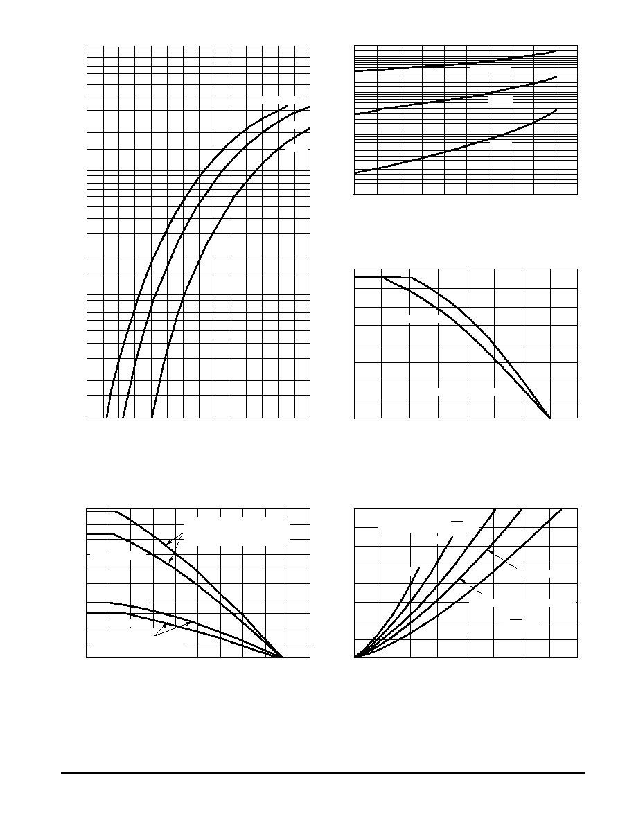
Figure 11. Typical Forward Voltage (Per Leg)
100
0.02
0.05
0.1
0.2
0.5
1
2
5
10
20
50
150
I R
, REVERSE CURRENT
(
A
)
╡
VR, REVERSE VOLTAGE (VOLTS)
Figure 12. Typical Reverse Current (Per Leg)
16
14
12
10
8
6
4
2
0
140
150
160
170
180
I F(A
V)
, A
VERAGE
FOR
W
ARD
CURRENT
(AMPS)
TC, CASE TEMPERATURE (
░
C)
Figure 13. Current Derating, Case (Per Leg)
dc
10
9
0
120
140
160
180
200
TA, AMBIENT TEMPERATURE (
░
C)
Figure 14. Current Derating, Ambient (Per Leg)
P
F(A
V)
,
A
VERAGE POWER DISSIP
A
TION
(W
A
TTS)
16
14
12
10
8
6
4
2
0
0
IF(AV), AVERAGE FORWARD CURRENT (AMPS)
Figure 15. Power Dissipation (Per Leg)
2
4
6
8
10
12
14
16
dc
I F(A
V)
, A
VERAGE
FOR
W
ARD
CURRENT
(AMPS)
100
░
C
25
░
C
TJ = 150
░
C
200
250
300
350
400
450
500
550
600
650
25
░
C
100
░
C
TJ = 150
░
C
SQUARE WAVE
RATED VOLTAGE APPLIED
dc
R
JA = 60
░
C/W
AS OBTAINED IN FREE AIR
WITH NO HEAT SINK.
SQUARE WAVE
SQUARE WAVE
dc
R
JA = 16
░
C/W AS OBTAINED
FROM A SMALL TO¡220
HEAT SINK.
20
40
60
80
100
20
10
(CAPACITIVE LOAD)
IPK
IAV
= 5
SQUARE WAVE
TJ = 125
░
C
IPK
IAV
=
(RESISTIVE¡INDUCTIVE LOAD)
200
8
7
6
5
4
3
2
1
0
MUR3020PT MUR3040PT MUR3060PT
5
Rectifier Device Data
0.01
0.02
0.05
0.1
0.2
0.5
1
0.01
0.02
0.05
0.1
0.2
0.5
1
2
5
10
20
50
100
200
500
1K
t, TIME (ms)
Figure 16. Thermal Response
D = 0.5
0.1
0.05
0.01
SINGLE PULSE
P(pk)
t1
t2
DUTY CYCLE, D = t1/t2
Z
JC(t) = r(t) R
JC
R
JC = 1.5
░
C/W MAX
D CURVES APPLY FOR POWER
PULSE TRAIN SHOWN
READ TIME AT T1
TJ(pk) ¡ TC = P(pk) Z
JC(t)
r(t), TRANSIENT
THERMAL
RESIST
ANCE
(NORMALIZED)
1K
10
20
50
100
200
500
1
2
5
10
20
50
100
VR, REVERSE VOLTAGE (VOLTS)
Figure 17. Typical Capacitance (Per Leg)
C, CAP
ACIT
ANCE
(pF)
TJ = 25
░
C

MUR3020PT MUR3040PT MUR3060PT
6
Rectifier Device Data
OUTLINE DIMENSIONS
CASE 340D¡02
ISSUE B
STYLE 2:
PIN 1. ANODE 1
2. CATHODE(S)
3. ANODE 2
4. CATHODE(S)
NOTES:
1. DIMENSIONING AND TOLERANCING PER ANSI
Y14.5M, 1982.
2. CONTROLLING DIMENSION: MILLIMETER.
A
D
V
G
K
S
L
U
B
Q
E
C
J
H
DIM
MIN
MAX
MIN
MAX
INCHES
MILLIMETERS
A
¡¡¡
20.35
¡¡¡
0.801
B
14.70
15.20
0.579
0.598
C
4.70
4.90
0.185
0.193
D
1.10
1.30
0.043
0.051
E
1.17
1.37
0.046
0.054
G
5.40
5.55
0.213
0.219
H
2.00
3.00
0.079
0.118
J
0.50
0.78
0.020
0.031
K
31.00 REF
1.220 REF
L
¡¡¡
16.20
¡¡¡
0.638
Q
4.00
4.10
0.158
0.161
S
17.80
18.20
0.701
0.717
U
4.00 REF
0.157 REF
V
1.75 REF
0.069
1
2
3
4
Motorola reserves the right to make changes without further notice to any products herein. Motorola makes no warranty, representation or guarantee regarding
the suitability of its products for any particular purpose, nor does Motorola assume any liability arising out of the application or use of any product or circuit, and
specifically disclaims any and all liability, including without limitation consequential or incidental damages. "Typical" parameters which may be provided in Motorola
data sheets and/or specifications can and do vary in different applications and actual performance may vary over time. All operating parameters, including "Typicals"
must be validated for each customer application by customer's technical experts. Motorola does not convey any license under its patent rights nor the rights of
others. Motorola products are not designed, intended, or authorized for use as components in systems intended for surgical implant into the body, or other
applications intended to support or sustain life, or for any other application in which the failure of the Motorola product could create a situation where personal injury
or death may occur. Should Buyer purchase or use Motorola products for any such unintended or unauthorized application, Buyer shall indemnify and hold Motorola
and its officers, employees, subsidiaries, affiliates, and distributors harmless against all claims, costs, damages, and expenses, and reasonable attorney fees
arising out of, directly or indirectly, any claim of personal injury or death associated with such unintended or unauthorized use, even if such claim alleges that
Motorola was negligent regarding the design or manufacture of the part. Motorola and are registered trademarks of Motorola, Inc. Motorola, Inc. is an Equal
Opportunity/Affirmative Action Employer.
Mfax is a trademark of Motorola, Inc.
How to reach us:
USA / EUROPE / Locations Not Listed: Motorola Literature Distribution;
JAPAN: Nippon Motorola Ltd.: SPD, Strategic Planning Office, 4¡32¡1,
P.O. Box 5405, Denver, Colorado 80217. 1¡303¡675¡2140 or 1¡800¡441¡2447
Nishi¡Gotanda, Shinagawa¡ku, Tokyo 141, Japan. 81¡3¡5487¡8488
Customer Focus Center: 1¡800¡521¡6274
Mfax
TM
: RMFAX0@email.sps.mot.com ¡ TOUCHTONE 1¡602¡244¡6609
ASIA/PACIFIC: Motorola Semiconductors H.K. Ltd.; 8B Tai Ping Industrial Park,
Motorola Fax Back System
¡ US & Canada ONLY 1¡800¡774¡1848
51 Ting Kok Road, Tai Po, N.T., Hong Kong. 852¡26629298
¡ http://sps.motorola.com/mfax/
HOME PAGE: http://motorola.com/sps/
MUR3020PT/D