Document Outline
- Introduction
- 33888 Simplified Application Diagram
- Features Comparison: 33888 and 33888A
- 33888 Simplified Internal Block Diagram
- Terminal Definitions for PQFN
- Terminal Definitions for PQFP
- Maximum Ratings
- Static Electrical Characteristics
- Dynamic Electrical Characteristics
- Timing Diagrams
- System/Application Information
- Introduction
- Functional Description
- Modes of Operation
- Package Information
- Applications
- Package Dimensions
- 36-Terminal PQFN
- 64-Terminal PQFP
MOTOROLA
SEMICONDUCTOR TECHNICAL DATA
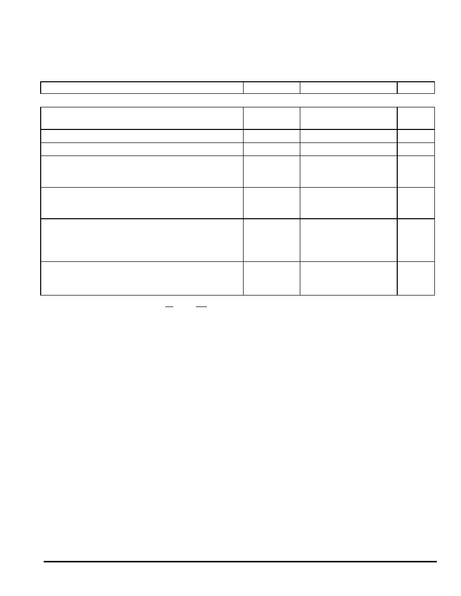
33888 Simplified Application Diagram
33888
33888A
This document contains certain information on a new product.
Specifications and information herein are subject to change without notice.
© Motorola, Inc. 2004
Document order number: MC33888
Rev 3.0, 10/2004
Product Preview
+5.0 V
+5.0 V
FSI
FS
MCU
A/D
A/D
CSNS0-1
CSNS2-3
WDIN
SPI
IHS0:IHS3
ILS
RST
V
DD
4
4
GND
V
PWR
LS4:LS11
HS3
HS2
HS1
HS0
Loads
8 x Relay or LED
33888
V
PWR
ORDERING INFORMATION
Device
Temperature
Range (T
A
)
Package
PC33888PNB/R2
-40∞C to 125∞C
36 PQFN
PC33888APNB/R2
MC33888FB/R2
64 PQFP
Quad High-Side and Octal Low-Side
Switch for Automotive
The 33888 is a single-package combination of a power die with four
discrete high-side MOSFETs (two 10 m
and two 40 m) and an integrated
IC control die consisting of eight low-side drivers (600 m
each) with
appropriate control, protection, and diagnostic features.
Programming, control, and diagnostics are accomplished using a 16-bit SPI
interface. Additionally, each high-side output has its own parallel input for
pulse-width modulation (PWM) control if desired. The low sides share a single
configurable direct input.
The 33888 is
available
i
n two power packages.
Features
∑ Dual 10 m
High Side, Dual 40 m High Side, Octal 600 m Low Side
∑ Full Operating Voltage of 6.0 V to 27 V
∑ SPI Control of High-Side Overcurrent Limit, High Side Current Sense,
Output OFF Open Load Detection, Output ON/OFF Control, Watchdog
Timeout
∑ SPI Reporting of Program Status and Fault
∑ High-Side Analog Current Feedback with Selectable Ratio
∑ Enhanced 16 V Reverse Polarity V
PWR
Protection
SOLID STATE RELAY FOR
AUTOMOTIVE APPLICATIONS
PNB SUFFIX
APNB SUFFIX
CASE 1438-06
36-TERMINAL PQFN
(12 x 12)
Bottom View
FB SUFFIX
CASE 1315-03
64-TERMINAL PQFP
Top View
F
r
e
e
s
c
a
l
e
S
e
m
i
c
o
n
d
u
c
t
o
r
,
I
Freescale Semiconductor, Inc.
For More Information On This Product,
Go to: www.freescale.com
n
c
.
.
.
33888
MOTOROLA ANALOG INTEGRATED CIRCUIT DEVICE DATA
2
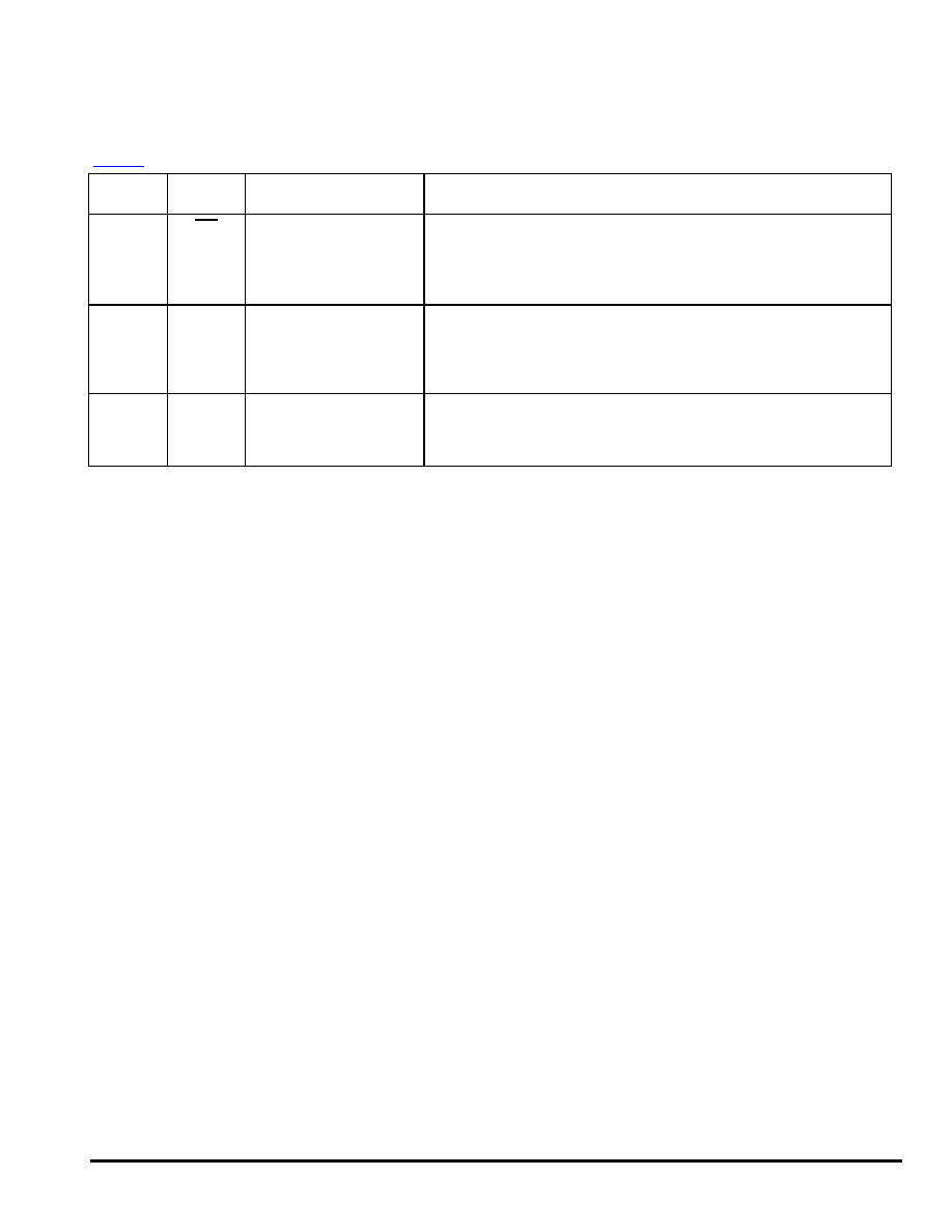
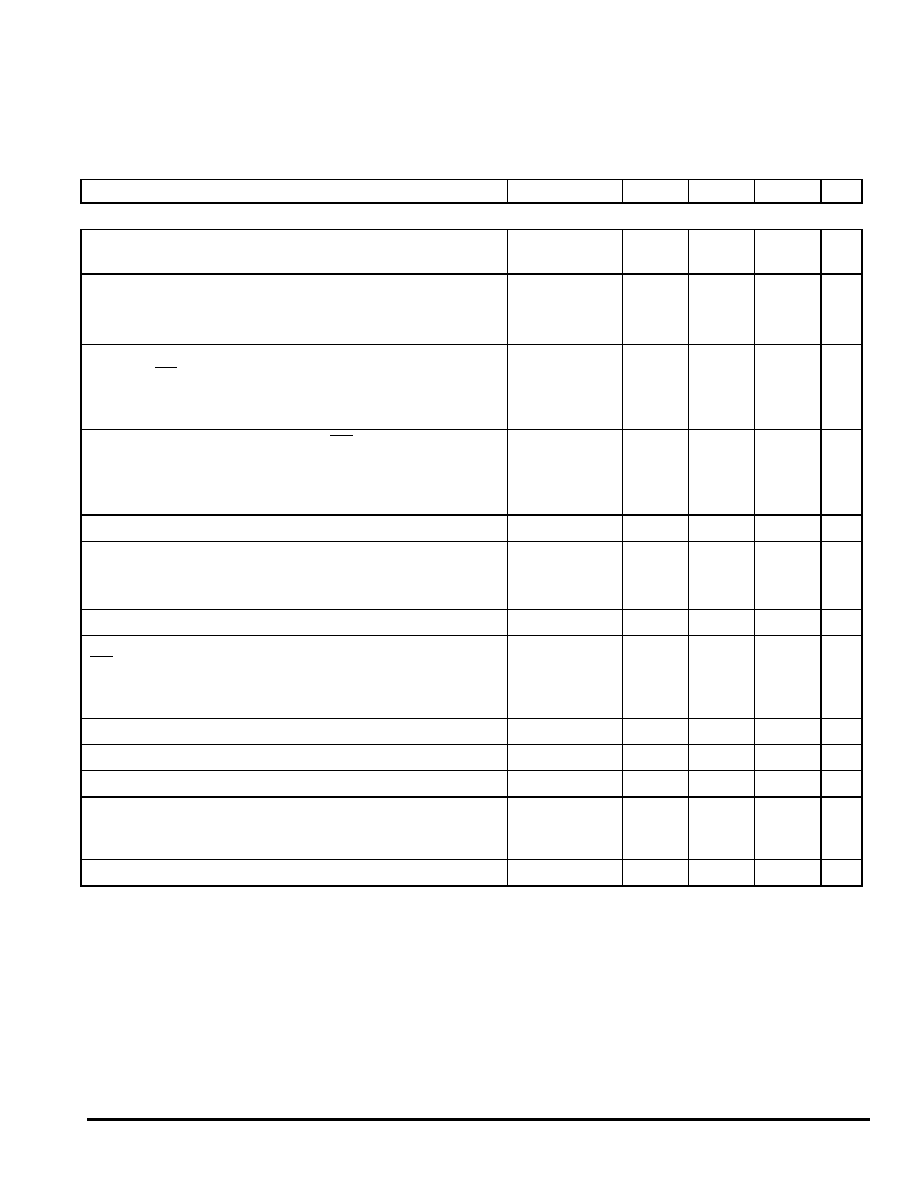
Table 1. Features Comparison: 33888 and 33888A
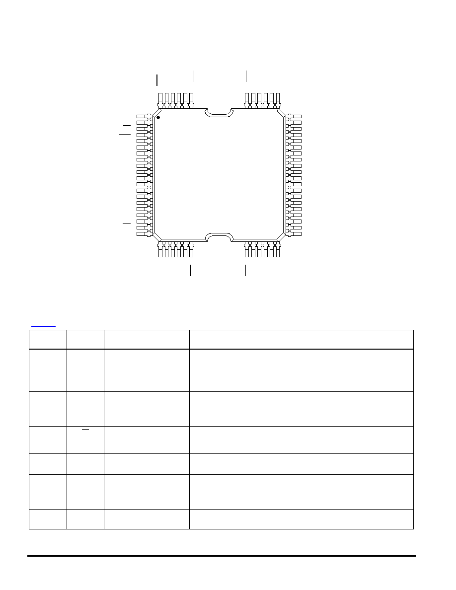
Figure 1. 33888 Simplified Internal Block Diagram
Parameter
Symbol
Condition
33888
33888A
For details,
see page
Undervoltage Low-Side Output Shutdown
V
PWRUV
≠
5.0 V
3.0 V
11
Low-Side Drain-to-Source ON Resistance
R
DS(ON)
V
PWR
= 4.5 V;
V
DD
= 3.5 V
Not specified
8.0
14
Recommended Frequency of SPI Operation
f
SPI
Extended Mode,
V
DD
= 3.4 V
Not specified
2.1 MHz
(max)
17
Watchdog
Overtemperature
Detection
Open Load
Detection
Logic
SPI
3.0 MHz
Selectable Current Limit
Internal
Regulator
Gate Driver
Over/Undervoltage
Protection
HS0
V
PWR
V
DD
CS
SCLK
SO
SI
RST
WAKE
FS
IN0
FSI
IN3
CSNS0-1
HS0
HS1
HS2
HS3
HS1
HS2
IN1
IN2
Selectable Output Current
Recopy (Analog MUX)
V
IC
V
IC
I
DWN
I
UP
I
DWN
R
DWN
Selectable Output Current
Recopy (Analog MUX)
Gate
Control
Clamp
Over-
temperature
I
LIM
Open Load
LS4
LS5
LS6
LS7
LS8
LS9
LS10
LS11
x 8
HS3
CSNS2-3
GND
10 m
Gate Control and Fault 10 m
Gate Control and Fault 40 m
Gate Control and Fault 40 m
ILS
WDIN
F
r
e
e
s
c
a
l
e
S
e
m
i
c
o
n
d
u
c
t
o
r
,
I
Freescale Semiconductor, Inc.
For More Information On This Product,
Go to: www.freescale.com
n
c
.
.
.
MOTOROLA ANALOG INTEGRATED CIRCUIT DEVICE DATA
33888
3
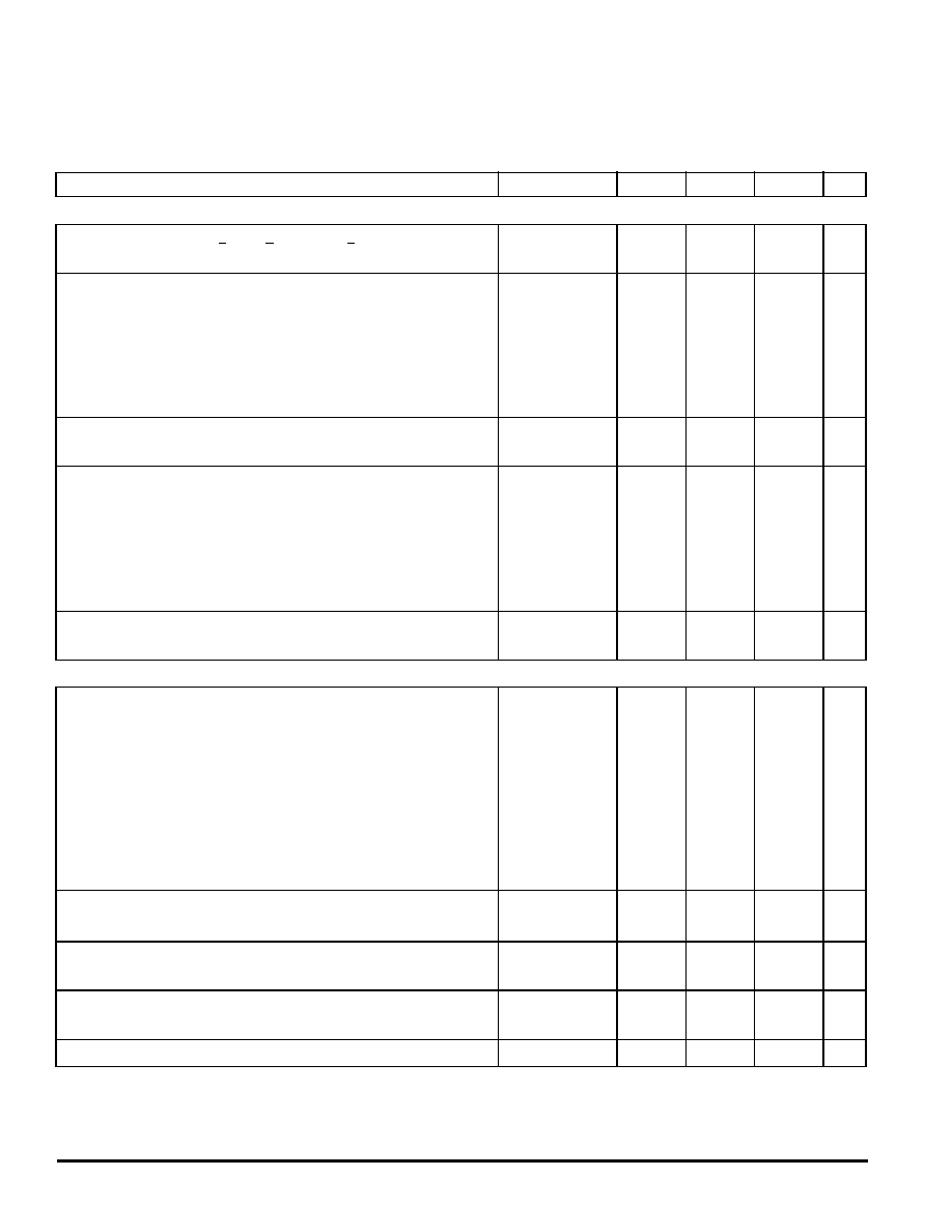
TERMINAL DEFINITIONS FOR PQFN
Functional descriptions of many of these terminals can be found in the System/Application Information section beginning on
page 19
.
Terminal
Terminal
Name
Formal Name
Definition
1
FS
Fault Status
(Active Low)
This output terminal is an open drain indication that goes active low when a fault
mode is detected by the device. Specific device fault indication is given via the SO
terminal.
2, 24
V
PWR
Positive Power Supply
These terminal connects to the positive power supply and are the source input of
operational power for the device.
3
6
8
10
LS4
LS6
LS8
LS10
Low-Side Output 4
Low-Side Output 6
Low-Side Output 8
Low-Side Output 10
Each low-side terminal is one 0.6
low-side output MOSFET drain, which pulls
current through the connected loads. Each of the outputs is actively clamped at
53 V. These outputs are current and thermal overload protected. Maximum steady
state current through each of these outputs is 500 mA.
4, 11, 15,
20, 32
GND
Ground
These terminals serve as the ground for the source of the low-side output
transistors as well as the logic portion of the device.
5
7
9
12
LS5
LS7
LS9
LS11
Low-Side Output 5
Low-Side Output 7
Low-Side Output 9
Low-Side Output 11
Each low-side terminal is one 0.6
low-side output MOSFET drain, which pulls
current through the connected loads. Each of the outputs is actively clamped at
53 V. These outputs are current and thermal overload protected. Maximum steady
state current through each of these outputs is 800 mA.
13
V
DD
Digital Drain Voltage (Power)
This is an external input terminal used to supply power to the SPI circuit.
Transparent Top View of Package
2
3
13
11
12
10
9
8
7
6
5
4
15
GND
17
18
19
21
20
22
35
34
33
32
31
30
23
24 V
PWR
25
26
27
28
29
1
36
WDIN
FSI
RST
WAKE
GND
IHS1
IHS0
CSNS0-1
SCLK
CS
SI
ILS
GND
IHS3
IHS2
CSNS2-3
HS3
HS
1
HS0
HS2
FS
V
PWR
LS4
GND
LS5
LS6
LS7
LS8
LS9
LS10
GND
LS11
V
DD
SO
14
Internally Connected to V
PWR
16
(Control Die)
(Power Die)
F
r
e
e
s
c
a
l
e
S
e
m
i
c
o
n
d
u
c
t
o
r
,
I
Freescale Semiconductor, Inc.
For More Information On This Product,
Go to: www.freescale.com
n
c
.
.
.
33888
MOTOROLA ANALOG INTEGRATED CIRCUIT DEVICE DATA
4
14
SO
Serial Output
This is an output terminal connected to the SPI Serial Data Input terminal of the
MCU or to the SI terminal of the next device in a daisy chain. This output will remain
tri-stated unless the device is selected by a low CS terminal. The output signal
generated will have CMOS logic levels and the output data will transition on the
rising edges of SCLK. The serial output data provides fault information for each
output and is returned MSB first when the device is addressed. OD11 through OD0
are output fault bits for outputs 11 through 0, respectively.
16
CS
Chip Select
(Active Low)
This is an input terminal connected to a chip select output of a microcontroller
(MCU). This IC controls which device is addressed (selected) by pulling the CS
terminal of the desired device logic Low, enabling the SPI communication with the
device, while other devices on the serial link keep their serial outputs tri-stated. This
input has an internal active pullup and requires CMOS logic levels.
17
SCLK
Serial Clock
This input terminal is connected to the SCLK terminal of the master MCU, which is
a bit (shift) clock for the SPI port. It transitions one time per bit transferred at an
operating frequency, f
SPI
, and is idle between command transfers. It is 50% duty
cycle and has CMOS logic levels. This signal is used to shift data to and from the
33888.
18
SI
Serial Input
This input terminal is connected to the SPI Serial Data Output terminal of the MCU
from which it receives output command data. This input has an internal active
pull-down and requires CMOS logic levels. The serial data transmitted on this line
is a 16-bit control command sent MSB first, which controls the twelve output
channels. Bits D3:D0 control the high-side outputs HS3:HS0, respectively. Bits
D11:D4 control the low-side outputs LS11:LS4, respectively. The MUC will ensure
that data is available on the falling edge of SCLK.
19
ILS
Low-Side Input
This input terminal is used to directly control a number of the low-side devices as
configured by SPI. This terminal may or may not be activated depending on the
configured state of the internal logic.
21
22
30
31
IHS3
IHS2
IHS0
IHS1
High-Side Input 3
High-Side Input 2
High-Side Input 0
High-Side Input 1
Each high-side input terminal is used to directly control only one designated high-
side output. These inputs may or may not be activated depending on the configured
state of the internal logic.
23
29
CSNS2-3
CSNS0-1
Current Sense 2-3
Current Sense 0-1
These terminals deliver a ratioed amount of the high-side output current that can be
used to generate signal ground referenced output voltages for use by the MCU.
Each respective CSNS terminal can be configured via SPI to deliver current from
either of the two assigned outputs, or the currents could be the sum of the two.
Current from HS0 and/or HS1 are sensed via CSNS0-1. Current from HS2 and/or
HS3 are sensed via CSNS2-3.
25
28
HS3
HS2
High-Side Output 3
High-Side Output 2
Each terminal is the source of a 40 m
MOSFET high-side driver, which delivers
current through the connected loads. These outputs can be controlled via SPI or
using the IHS terminals depending on the internal configuration. These outputs are
current limited and thermally protected. During fail-safe mode, output HS2 will be
turned on until the device is reinitialized and then immediately followed by normal
operation.
26
27
HS1
HS0
High-Side Output 1
High-Side Output 0
Each terminal is the source of a 10 m
MOSFET high-side driver, which delivers
current through the connected loads. These outputs can be controlled via SPI or
using the IHS terminals depending on the internal configuration. These outputs are
current limited and thermally protected. During fail-safe mode, output HS0 will be
turned on until the device is reinitialized and then immediately followed by normal
operation.
33
WAKE
Wake
This terminal is used to input a logic [1] signal in order to enable the watchdog timer
function. An internal clamp protects the terminal from high voltages when current is
limited with an external resistor. This input has a passive internal pulldown.
TERMINAL DEFINITIONS FOR PQFN (continued)
Functional descriptions of many of these terminals can be found in the System/Application Information section beginning on
page 19
.
Terminal
Terminal
Name
Formal Name
Definition
F
r
e
e
s
c
a
l
e
S
e
m
i
c
o
n
d
u
c
t
o
r
,
I
Freescale Semiconductor, Inc.
For More Information On This Product,
Go to: www.freescale.com
n
c
.
.
.
MOTOROLA ANALOG INTEGRATED CIRCUIT DEVICE DATA
33888
5
34
RST
Reset (Active Low)
This input terminal is used to initialize the device configuration and fault registers,
as well as place the device in a low current standby mode. This terminal also starts
the watchdog timeout when transitioned from logic [0] to logic [1]. This terminal
should not be allowed to be at logic [1] until V
DD
is in regulation. This input has an
internal passive pulldown.
35
FSI
Fail-Safe Input
The Fail-Safe input terminal level determines the state of the outputs after a
watchdog timeout occurs. This terminal has an internal pullup. If the FSI terminal is
left to float to a logic [1], then HS0 and HS2 will turn on when in the Fail-Safe state.
If the FSI terminal is tied to GND, the watchdog circuit and fail-safe operation will be
disabled, thus allowing operation without a watchdog signal.
36
WDIN
Watchdog Input
This input terminal is a CMOS logic level input that is used to monitor system
operation. If the incoming watchdog signal does not transition within the normal
watchdog timeout range, the device will operate in the Fail-Safe mode. This input
has an active internal pulldown.
TERMINAL DEFINITIONS FOR PQFN (continued)
Functional descriptions of many of these terminals can be found in the System/Application Information section beginning on
page 19
.
Terminal
Terminal
Name
Formal Name
Definition
F
r
e
e
s
c
a
l
e
S
e
m
i
c
o
n
d
u
c
t
o
r
,
I
Freescale Semiconductor, Inc.
For More Information On This Product,
Go to: www.freescale.com
n
c
.
.
.
33888
MOTOROLA ANALOG INTEGRATED CIRCUIT DEVICE DATA
6
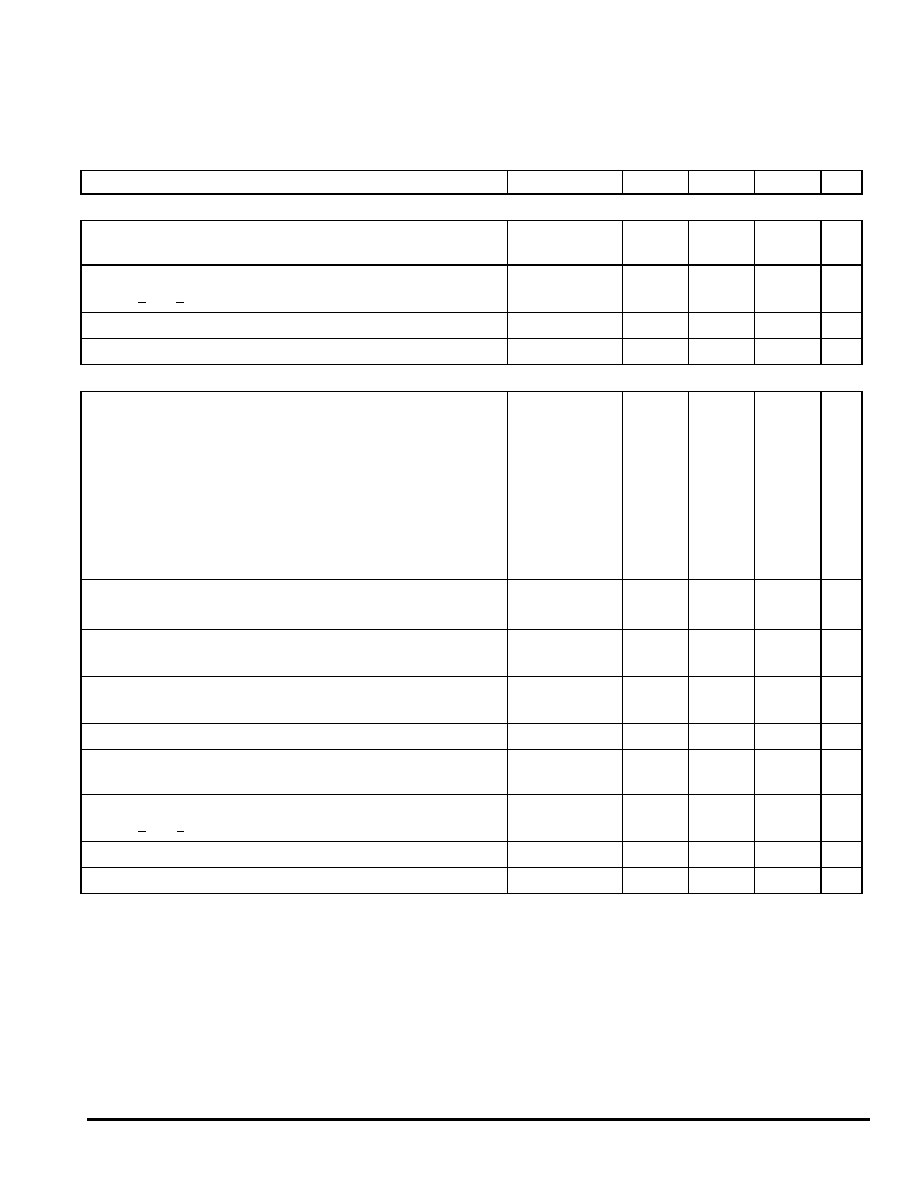
TERMINAL DEFINITIONS FOR PQFP
Functional descriptions of many of these terminals can be found in the System/Application Information section beginning on
page 19
.
Terminal
Terminal
Name
Formal Name
Definition
1
FSI
Fail-Safe Input
The Fail-Safe input terminal level determines the state of the outputs after a
watchdog timeout occurs. This terminal has an internal pullup. If the FSI terminal is
left to float to a logic [1], then HS0 and HS2 will turn on when in the Fail-Safe state.
If the FSI terminal is tied to GND, the watchdog circuit and fail-safe operation will be
disabled, thus allowing operation without a watchdog signal.
2
WDIN
Watchdog Input
This input terminal is a CMOS logic level input that is used to monitor system
operation. If the incoming watchdog signal does not transition within the normal
watchdog timeout range, the device will operate in the Fail-Safe mode. This input
has an active internal pulldown.
3
FS
Fault Status
(Active Low)
This output terminal is an open drain indication that goes active low when a fault
mode is detected by the device. Specific device fault indication is given via the SO
terminal.
4, 26, 27,
58, 59
V
PWR
Positive Power Supply
These terminal connects to the positive power supply and are the source input of
operational power for the device.
5
8
11
14
LS4
LS6
LS8
LS10
Low-Side Output 4
Low-Side Output 6
Low-Side Output 8
Low-Side Output 10
Each low-side terminal is one 0.6
low-side output MOSFET drain, which pulls
current through the connected loads. Each of the outputs is actively clamped at
53 V. These outputs are current and thermal overload protected. Maximum steady
state current through each of these outputs is 500 mA.
6, 9, 12, 15
GND
Ground
These terminals serve as the ground for the source of the low-side output
transistors as well as the logic portion of the device.
FSI
1
GND
LS5
LS6
LS8
LS11
V
DD
SO
CS
SCLK
GND
LS9
LS10
GND
GND
LS7
LS4
V
PWR
FS
WDIN
NC
HS0
HS0
HS0
HS1
HS1
HS1
NC
NC
NC
HS1
HS1
HS1
HS1
HS0
HS0
HS0
HS0
NC
NC
V
PW
R
NC
NC
NC
HS2
HS2
SI
V
PW
R
CSN
S
2-
3
IHS2
IHS3
ILS
V
PW
R
NC
NC
NC
HS3
HS3
14
15
16
17
18
19
20
8
9
10
12
13
11
4
5
6
7
3
2
64
61
60
59
62
63
21
24
25
26
23
22
27
30
31
32
29
28
52
39
38
37
36
35
34
33
45
44
43
41
40
42
49
48
47
46
50
51
58
55
54
53
56
57
RST
V
PW
R
CSNS0-
1
IHS0
IHS1
WAKE
F
r
e
e
s
c
a
l
e
S
e
m
i
c
o
n
d
u
c
t
o
r
,
I
Freescale Semiconductor, Inc.
For More Information On This Product,
Go to: www.freescale.com
n
c
.
.
.
MOTOROLA ANALOG INTEGRATED CIRCUIT DEVICE DATA
33888
7
7
10
13
16
LS5
LS7
LS9
LS11
Low-Side Output 5
Low-Side Output 7
Low-Side Output 9
Low-Side Output 11
Each low-side terminal is one 0.6
low-side output MOSFET drain, which pulls
current through the connected loads. Each of the outputs is actively clamped at
53 V. These outputs are current and thermal overload protected. Maximum steady
state current through each of these outputs is 800 mA.
17
V
DD
Digital Drain Voltage (Power)
This is an external input terminal used to supply power to the SPI circuit.
18
SO
Serial Output
This is an output terminal connected to the SPI Serial Data Input terminal of the
MCU or to the SI terminal of the next device in a daisy chain. This output will remain
tri-stated unless the device is selected by a low CS terminal. The output signal
generated will have CMOS logic levels and the output data will transition on the
rising edges of SCLK. The serial output data provides fault information for each
output and is returned MSB first when the device is addressed. OD11 through OD0
are output fault bits for outputs 11 through 0, respectively.
19
CS
Chip Select
(Active Low)
This is an input terminal connected to a chip select output of a microcontroller
(MCU). This IC controls which device is addressed (selected) by pulling the CS
terminal of the desired device logic Low, enabling the SPI communication with the
device, while other devices on the serial link keep their serial outputs tri-stated. This
input has an internal active pullup and requires CMOS logic levels.
20
SCLK
Serial Clock
This input terminal is connected to the SCLK terminal of the master MCU, which is
a bit (shift) clock for the SPI port. It transitions one time per bit transferred at an
operating frequency, f
SPI
, and is idle between command transfers. It is 50% duty
cycle and has CMOS logic levels. This signal is used to shift data to and from the
33888.
21
SI
Serial Input
This input terminal is connected to the SPI Serial Data Output terminal of the MCU
from which it receives output command data. This input has an internal active
pull-down and requires CMOS logic levels. The serial data transmitted on this line
is a 16-bit control command sent MSB first, which controls the twelve output
channels. Bits D3:D0 control the high-side outputs HS3:HS0, respectively. Bits
D11:D4 control the low-side outputs LS11:LS4, respectively. The MUC will ensure
that data is available on the falling edge of SCLK.
22
ILS
Low-Side Input
This input terminal is used to directly control a number of the low-side devices as
configured by SPI. This terminal may or may not be activated depending on the
configured state of the internal logic.
23
24
61
62
IHS3
IHS2
IHS0
IHS1
High-Side Input 3
High-Side Input 2
High-Side Input 0
High-Side Input 1
Each high-side input terminal is used to directly control only one designated high-
side output. These inputs may or may not be activated depending on the configured
state of the internal logic.
25
60
CSNS2-3
CSNS0-1
Current Sense 2-3
Current Sense 0-1
These terminals deliver a ratioed amount of the high-side output current that can be
used to generate signal ground referenced output voltages for use by the MCU.
Each respective CSNS terminal can be configured via SPI to deliver current from
either of the two assigned outputs, or the currents could be the sum of the two.
Current from HS0 and/or HS1 are sensed via CSNS0-1. Current from HS2 and/or
HS3 are sensed via CSNS2-3.
28, 29
56, 57
HS3
HS2
High-Side Output 3
High-Side Output 2
Each terminal is the source of a 40 m
MOSFET high-side driver, which delivers
current through the connected loads. These outputs can be controlled via SPI or
using the IHS terminals depending on the internal configuration. These outputs are
current limited and thermally protected. During fail-safe mode, output HS2 will be
turned on until the device is reinitialized and then immediately followed by normal
operation.
30≠35,
50≠55
NC
Not Connected
These terminals are not connected internally.
TERMINAL DEFINITIONS FOR PQFP (continued)
Functional descriptions of many of these terminals can be found in the System/Application Information section beginning on
page 19
.
Terminal
Terminal
Name
Formal Name
Definition
F
r
e
e
s
c
a
l
e
S
e
m
i
c
o
n
d
u
c
t
o
r
,
I
Freescale Semiconductor, Inc.
For More Information On This Product,
Go to: www.freescale.com
n
c
.
.
.
33888
MOTOROLA ANALOG INTEGRATED CIRCUIT DEVICE DATA
8
36≠42
43≠49
HS1
HS0
High-Side Output 1
High-Side Output 0
Each terminal is the source of a 10 m
MOSFET high-side driver, which delivers
current through the connected loads. These outputs can be controlled via SPI or
using the IHS terminals depending on the internal configuration. These outputs are
current limited and thermally protected. During fail-safe mode, output HS0 will be
turned on until the device is reinitialized and then immediately followed by normal
operation.
63
WAKE
Wake
This terminal is used to input a logic [1] signal in order to enable the watchdog timer
function. An internal clamp protects the terminal from high voltages when current is
limited with an external resistor. This input has a passive internal pulldown.
64
RST
Reset (Active Low)
This input terminal is used to initialize the device configuration and fault registers,
as well as place the device in a low current standby mode. This terminal also starts
the watchdog timeout when transitioned from logic [0] to logic [1]. This terminal
should not be allowed to be at logic [1] until V
DD
is in regulation. This input has an
internal passive pulldown.
TERMINAL DEFINITIONS FOR PQFP (continued)
Functional descriptions of many of these terminals can be found in the System/Application Information section beginning on
page 19
.
Terminal
Terminal
Name
Formal Name
Definition
F
r
e
e
s
c
a
l
e
S
e
m
i
c
o
n
d
u
c
t
o
r
,
I
Freescale Semiconductor, Inc.
For More Information On This Product,
Go to: www.freescale.com
n
c
.
.
.
MOTOROLA ANALOG INTEGRATED CIRCUIT DEVICE DATA
33888
9
MAXIMUM RATINGS
All voltages are with respect to ground unless otherwise noted.
Rating
Symbol
Value
Unit
ELECTRICAL RATINGS
Power Supply Voltage
Steady State
V
PWR
-16 to 41
V
Input Terminal Voltage
(Note 1)
V
IN
-0.3 to 7.0
V
WAKE Input Terminal Clamp Current
I
WICI
2.5
mA
Continuous per Output Current
(Note 2)
Low-Sides 4, 6, 8, 10
Low-Sides 5, 7, 9, 11
I
OUTLS
500
800
mA
Continuous per Output Current
(Note 3)
High-Sides 0, 1
High-Sides 2, 3
I
OUTHS
10
5.0
A
Output Clamp Energy
High-Sides 0, 1
(Note 4)
High-Sides 2, 3
(Note 5)
Low-Sides
(Note 6)
E
HS
E
HS
E
LS
450
120
50
mJ
ESD Voltage
Human Body Model
(Note 7)
Machine Model
(Note 8)
V
ESD1
V
ESD2
±2000
±200
V
Notes
1.
Exceeding voltage limits on SCLK, SI, CS, WDIN, RST, IHS, FSI, or ILS terminals may cause a malfunction or permanent damage to the
device.
2.
Continuous low-side output current rating so long as maximum junction temperature is not exceeded. Operation at 125∞C ambient
temperature will require calculation of maximum output current using package thermal resistance.
3.
Continuous high-side output current rating so long as maximum junction temperature is not exceeded. Operation at 125∞C ambient
temperature will require calculation of maximum output current using package thermal resistance.
4.
Active HS0 and HS1 clamp energy using the following conditions: single nonrepetitive pulse, V
PWR
= 16.0 V, L = 40 mH, T
J
= 150∞C.
5.
Active HS2 and HS3 clamp energy using the following conditions: single nonrepetitive pulse, V
PWR
= 16.0 V, L = 10 mH, T
J
= 150∞C.
6.
Active low-side clamp energy using the following conditions: single nonrepetitive pulse, 450 mA, T
J
= 150∞C.
7.
ESD1 testing is performed in accordance with the Human Body Model (C
ZAP
=100 pF, R
ZAP
= 1500
).
8.
ESD2 testing is performed in accordance with the Machine Model (C
ZAP
= 200 pF, R
ZAP
= 0
).
F
r
e
e
s
c
a
l
e
S
e
m
i
c
o
n
d
u
c
t
o
r
,
I
Freescale Semiconductor, Inc.
For More Information On This Product,
Go to: www.freescale.com
n
c
.
.
.

33888
MOTOROLA ANALOG INTEGRATED CIRCUIT DEVICE DATA
10
THERMAL RATINGS
Operating Temperature
Ambient
Junction
T
A
T
J
-40 to 125
-40 to 150
∞
C
Storage Temperature
T
STG
-55 to 150
∞C
Control Die Thermal Resistance
(Note 9)
PQFP
One Low-Side ON
Two Low-Side ON
Three Low-Side ON
Four Low Side ON
All Low-Sides ON
PQFN
One Low-Side ON
Two Low-Side ON
Three Low-Side ON
Four Low Side ON
All Low-Sides ON
R
CJC
12.5
9.3
7.3
5.9
3.2
8.6
6.0
4.6
3.8
2.0
∞C/W
Power Die Thermal Resistance
(Note 9)
PQFP
One High-Side 2, 3 ON
All High-Sides ON
PQFN
One High-Side 2, 3 ON
All High-Sides ON
R
PJC
0.5
0.15
0.5
0.1
∞C/W
Thermal Resistance, Junction to Ambient, Natural Convection, Four-Layer
Board
(Note 9)
PQFP
PQFN
R
JA
33
37
∞C/W
Peak Terminal Reflow Temperature During Solder Mounting
(Note 10)
PQFP
PQFN
T
SOLDER
225
240
∞
C
Notes
9.
Board dimensions are 8.0 cm x 8.0 cm x 1.5 mm with a 300 mm
2
copper area on the bottom layer.
10.
Terminal soldering temperature limit is 10 seconds maximum duration. Not designed for immersion soldering. Exceeding these limits may
cause malfunction or permanent damage to the device.
MAXIMUM RATINGS (continued)
All voltages are with respect to ground unless otherwise noted.
Rating
Symbol
Value
Unit
F
r
e
e
s
c
a
l
e
S
e
m
i
c
o
n
d
u
c
t
o
r
,
I
Freescale Semiconductor, Inc.
For More Information On This Product,
Go to: www.freescale.com
n
c
.
.
.
MOTOROLA ANALOG INTEGRATED CIRCUIT DEVICE DATA
33888
11
STATIC ELECTRICAL CHARACTERISTICS
Characteristics noted under conditions 6.0 V
V
PWR
27 V, 4.5 V
V
DD
5.5 V, -40
∞C
T
J
150
∞C unless otherwise noted. Typical
values noted reflect the approximate parameter mean at T
A
= 25
∞C under nominal conditions unless otherwise noted.
Characteristic
Symbol
Min
Typ
Max
Unit
POWER INPUT
Supply Voltage Range
Fully Operational
V
PWR
6.0
≠
27
V
V
PWR
Supply Current
T
J
> 125∞C
T
J
125∞C
I
PWR(ON)
≠
≠
17
≠
25
20
mA
V
PWR
Standby Current (All Outputs OFF, Open Load Detection Disabled,
WAKE = H, RST = H)
T
J
> 125∞C
T
J
125∞C
I
PWR(SBY)
≠
≠
4.2
2.9
7.0
5.0
mA
Sleep State Supply Current (V
PWR
< 12.6 V, RST < 0.5 V, WAKE < 0.5 V,
HS[0:3] = 0 V)
(Note 11)
T
J
= 85∞C
T
J
= 25∞C
I
PWR(SS)
≠
≠
≠
1.0
80
25
µA
Logic Supply Voltage Range
V
DD
4.5
5.0
5.5
V
Logic Supply Current
T
J
> 125∞C
T
J
125∞C
I
DD(ON)
≠
≠
4.2
2.9
7.0
5.0
mA
Logic Supply Sleep State Current
I
DD(SS)
≠
≠
5.0
µA
Sleep State Low-Side Output Leakage Current (per Low-Side Output,
RST
= LOW)
T
J
= 85∞C
T
J
= 25∞C
I
SLK(SS)
≠
≠
≠
≠
3.0
1.0
µA
Overvoltage Shutdown
Threshold
V
PWROV
28
.
5
32
36
V
Overvoltage Shutdown Hysteresis
V
PWROV(HYS)
0.2
0.6
1.5
V
Undervoltage High-Side Output Shutdown
(Note 12)
V
PWRUV
5.0
5.6
6.0
V
Undervoltage Low-Side Output Shutdown
APNB Suffix Only
(Note 12)
PNB and FB Suffixes
V
PWRUV
3.0
5.0
4.0
5.6
4.4
6.0
V
Undervoltage High-Side Shutdown Hysteresis
V
PWRUV(HYS)
0.1
0.3
0.5
V
Notes
11.
This parameter is tested at 125∞C with a maximum value of 10
µA.
12.
SPI/IO and internal logic operational. Outputs will recover in instructed state when V
PWR
voltage level returns to normal as long as the level
does not go below V
PWRUV
.
F
r
e
e
s
c
a
l
e
S
e
m
i
c
o
n
d
u
c
t
o
r
,
I
Freescale Semiconductor, Inc.
For More Information On This Product,
Go to: www.freescale.com
n
c
.
.
.
33888
MOTOROLA ANALOG INTEGRATED CIRCUIT DEVICE DATA
12
POWER INPUT (continued)
Current Sense Ratio (9.0 V < V
PWR
< 16 V, CSNS < 4.5 V)
CSNS0-1/HS0, CSNS0-1/HS1
C
SR[0:1]
≠
1/1400
≠
≠
Current Sense Ratio (C
SR[0:1]
) Accuracy
HS[0:1] Output Current
1.0 A
2.0 A
5.0 A
6.5 A
10 A
C
SR[0:1]_ACC
-35
-19
-14
-12
-12
≠
≠
≠
≠
≠
35
19
14
12
12
%
Current Sense Ratio (V
PWR
= 9.0 V ≠ 16 V, CSNS < 4.5 V)
CSNS2-3/HS2, CSNS2-3/HS3
C
SR
≠
1/880
≠
≠
Current Sense Ratio (C
SR[2:3]
) Accuracy
HS[2:3] Output Current
0.5 A
1.0 A
3.0 A
3.7 A
5.0 A
C
SR[2:3]_ACC
-30
-19
-13.5
-12
-9.0
≠
≠
≠
≠
≠
30
19
13.5
12
9.0
%
Current Sense Clamp Voltage
I
CNS
= 15 mA Generated by the Device
V
SENSE
4.5
6.0
7.0
V
HS0 AND HS1 POWER OUTPUTS
Drain-to-Source ON Resistance (I
OUT
= 5.5 A)
T
J
= 25∞C
V
PWR
= 6.0 V
V
PWR
= 9.0 V
V
PWR
= 13 V
T
J
= 150∞C
V
PWR
= 6.0 V
V
PWR
= 9.0 V
V
PWR
= 13 V
R
DS(ON)
≠
≠
≠
≠
≠
≠
≠
≠
≠
≠
≠
≠
0.02
0.01
0.01
0.034
0.017
0.017
Reverse Battery Source-to-Drain ON Resistance (I
OUT
= -5.5 A, T
J
= 25∞C)
V
PWR
= -12 V
R
DS(ON)REV
≠
≠
0.02
Output Self-Limiting Peak Current
Outputs ON, V
OUT
= V
PWR
-2.0 V
I
LIM(PK)
33
49
66
A
Output Self-Limiting Sustain Current
Outputs ON, V
OUT
= V
PWR
-2.0 V
I
LIM(SUS)
13
25
34
A
Open Load Detection Current
(Note 13)
I
OLDC
30
≠
100
µA
Notes
13.
Output OFF Open Load Detection Current is the current required to flow through the load for the purpose of detecting the existence of an
open load condition when the specific output is commanded OFF.
STATIC ELECTRICAL CHARACTERISTICS (continued)
Characteristics noted under conditions 6.0 V
V
PWR
27 V, 4.5 V
V
DD
5.5 V, -40
∞C
T
J
150
∞C unless otherwise noted. Typical
values noted reflect the approximate parameter mean at T
A
= 25
∞C under nominal conditions unless otherwise noted.
Characteristic
Symbol
Min
Typ
Max
Unit
F
r
e
e
s
c
a
l
e
S
e
m
i
c
o
n
d
u
c
t
o
r
,
I
Freescale Semiconductor, Inc.
For More Information On This Product,
Go to: www.freescale.com
n
c
.
.
.
MOTOROLA ANALOG INTEGRATED CIRCUIT DEVICE DATA
33888
13
HS0 AND HS1 POWER OUTPUTS (continued)
Output Fault Detection Threshold
(Note 14)
Output Programmed OFF
V
OFD(THRES)
2.0
3.0
4.0
V
Output Negative Clamp Voltage
0.5 A <
I
OUT
< 2.0 A, Output OFF
V
CL
-20
≠
≠
V
Overtemperature Shutdown (Outputs OFF)
(Note 15)
T
SD
160
175
190
∞C
Overtemperature Shutdown Hysteresis
(Note 15)
T
SD(HYS)
10
≠
30
∞C
HS2 AND HS3 POWER OUTPUTS
Drain-to-Source ON Resistance (I
OUT
= 4.5 A)
T
J
= 25∞C
V
PWR
= 6.0 V
V
PWR
= 9.0 V
V
PWR
= 13 V
T
J
= 150∞C
V
PWR
= 6.0 V
V
PWR
= 9.0 V
V
PWR
= 13 V
R
DS(ON)
≠
≠
≠
≠
≠
≠
≠
≠
≠
≠
≠
≠
0.08
0.04
0.04
0.136
0.068
0.068
Reverse Battery Source-to-Drain ON Resistance (I
OUT
= 4.5 A, T
J
= 25∞C)
V
PWR
= -12 V
R
DS(ON)REV
≠
≠
0.08
Output Self-Limiting Peak Current
Outputs ON, V
OUT
= V
PWR
-2.0 V
I
LIM(PK)
15
23
35
A
Output Self-Limiting Sustain Current
Outputs ON, V
OUT
= V
PWR
-2.0 V
I
LIM(SUS)
6.0
10
15
A
Open Load Detection Current
(Note 16)
I
OLDC
25
≠
100
µA
Output Fault Detection Threshold
(Note 17)
Outputs Programmed OFF
V
OFD(THRES)
2.0
3.0
4.0
V
Output Negative Clamp Voltage
0.5 A < I
OUT
< 2.0 A, Outputs OFF
V
CL
-20
≠
≠
V
Overtemperature Shutdown (Outputs OFF)
(Note 18)
T
SD
160
170
190
∞C
Overtemperature Shutdown Hysteresis
(Note 18)
T
SD(HYS)
10
≠
30
∞C
Notes
14.
Output fault detection threshold with outputs programmed OFF. For the Low-Side Outputs, fault detection thresholds are the same for output
open and battery shorts.
15.
Guaranteed by design. Not production tested.
16.
Output OFF Open Load Detection Current is the current required to flow through the load for the purpose of detecting the existence of an
open load condition when the specific output is commanded OFF.
17.
Output fault detection threshold with outputs programmed OFF.
18.
Guaranteed by design. Not production tested.
STATIC ELECTRICAL CHARACTERISTICS (continued)
Characteristics noted under conditions 6.0 V
V
PWR
27 V, 4.5 V
V
DD
5.5 V, -40
∞C
T
J
150
∞C unless otherwise noted. Typical
values noted reflect the approximate parameter mean at T
A
= 25
∞C under nominal conditions unless otherwise noted.
Characteristic
Symbol
Min
Typ
Max
Unit
F
r
e
e
s
c
a
l
e
S
e
m
i
c
o
n
d
u
c
t
o
r
,
I
Freescale Semiconductor, Inc.
For More Information On This Product,
Go to: www.freescale.com
n
c
.
.
.
33888
MOTOROLA ANALOG INTEGRATED CIRCUIT DEVICE DATA
14
LOW-SIDE POWER OUTPUTS
Drain-to-Source ON Resistance (I
OUT
= 0.3 A)
T
J
= 25∞C
V
PWR
= 4.5 V; V
DD
= 3.5 V, 33888A Only
V
PWR
= 6.0 V
V
PWR
= 9.0 V
V
PWR
= 13 V
T
J
= 150∞C
V
PWR
= 4.5 V; V
DD
= 3.5 V, 33888A Only
V
PWR
= 6.0 V
V
PWR
= 9.0 V
V
PWR
= 13 V
R
DS(ON)
≠
≠
≠
≠
≠
≠
≠
≠
≠
≠
≠
≠
≠
≠
≠
≠
8.0
1.0
0.7
0.6
8.0
1.8
1.1
0.9
Output Self-Limiting Current (Outputs Programmed ON, V
OUT
= 3.0 V)
Low-Side 4, 6, 8, 10
Low-Side 5, 7, 9, 11
I
LIM
0.5
0.8
0.9
1.3
1.5
2.0
A
Output OFF Open Load Detection Current
(Note 19)
Output Programmed OFF, V
OUT
= 3.0 V
I
OLDC
25
50
100
µA
Output Fault Detection Threshold
(Note 20)
Output Programmed OFF
V
OFD(THRES)
2.0
3.0
4.0
V
Output Clamp Voltage
2.0 mA < I
OUT
< 200 mA, Outputs OFF
V
CL
41
53
60
V
Low-Side Body Diode Voltage (I = -300 mA, T
J
= 125∞C)
V
BD
0.5
0.7
0.9
V
Overtemperature Shutdown (Outputs OFF)
(Note 21)
T
LIM
160
170
190
∞C
Overtemperature Shutdown Hysteresis
(Note 21)
T
LIM(HYS)
10
20
30
∞C
Notes
19.
Output OFF Open Load Detection Current is the current required to flow through the load for the purpose of detecting the existence of an
open load condition when the specific output is commanded OFF.
20.
Output fault detection threshold with outputs programmed OFF. For the low-side outputs, fault detection thresholds are the same for output
open and battery shorts.
21.
Guaranteed by design. Not production tested.
STATIC ELECTRICAL CHARACTERISTICS (continued)
Characteristics noted under conditions 6.0 V
V
PWR
27 V, 4.5 V
V
DD
5.5 V, -40
∞C
T
J
150
∞C unless otherwise noted. Typical
values noted reflect the approximate parameter mean at T
A
= 25
∞C under nominal conditions unless otherwise noted.
Characteristic
Symbol
Min
Typ
Max
Unit
F
r
e
e
s
c
a
l
e
S
e
m
i
c
o
n
d
u
c
t
o
r
,
I
Freescale Semiconductor, Inc.
For More Information On This Product,
Go to: www.freescale.com
n
c
.
.
.
MOTOROLA ANALOG INTEGRATED CIRCUIT DEVICE DATA
33888
15
CONTROL INTERFACE
Input Logic High Voltage
(Note 22)
V
IH
0.7 V
DD
≠
≠
V
Input Logic Low Voltage
(Note 22)
V
IL
≠
≠
1.0
V
Input Logic Voltage Hysteresis (SI, CS, SCLK, IHS[0:3], ILS)
(Note 23)
V
IN(HYS)
100
350
750
mV
Input Logic Pulldown Current (SI, SCLK, IHS[0:3], ILS, WDIN)
I
DWN
5.0
≠
20
µA
Input Logic Pulldown Resistor (WAKE, RST)
R
DWN
100
200
400
k
Input Logic Pullup Current (CS, V
IN
= 0.7 V
DD
)
(Note 24)
I
UPC
5.0
≠
20
µA
Input Logic Pullup Current (FSI, V
IN
= 3.5 V)
I
UPF
5.0
≠
20
µA
Wake Input Clamp Voltage (I
WICI
< 2.5 mA)
(Note 25)
V
WIC
7.0
≠
14
V
Wake Input Forward Voltage (I
WICI
= -2.5 mA)
V
WIF
-2.0
≠
-0.3
V
SO High-State Output Voltage (I
OH
= 1.0 mA)
V
SOH
0.8 V
DD
≠
≠
V
FS
, SO Low-State Output Voltage (I
OL
= -1.6 mA)
V
SOL
≠
0.2
0.4
V
SO Tri-State Leakage Current (CS
3.5 V)
I
SOLK
-5.0
0
5.0
µA
Input Capacitance
(Note 26)
C
IN
≠
4.0
12
pF
SO, FS Tri-State Capacitance
(Note 23)
C
SO
≠
≠
20
pF
Notes
22.
Upper and lower logic threshold voltage range applies to SI, CS, SCLK, RST, IHS[0:3], ILS, WAKE, and WDIN input signals. The WAKE,
FSI, and RST signals are derived from an internal supply.
23.
Parameter is guaranteed by design but is not production tested.
24.
CS
is pulled up to V
DD
.
25.
The current must be limited by a series resistor when using voltages higher than the W
ICV
.
26.
Input capacitance of SI, CS, SCLK, RST, IHS[0:3], ILS, WAKE, and WDIN. This parameter is guaranteed by process monitoring but is not
production tested.
STATIC ELECTRICAL CHARACTERISTICS (continued)
Characteristics noted under conditions 6.0 V
V
PWR
27 V, 4.5 V
V
DD
5.5 V, -40
∞C
T
J
150
∞C unless otherwise noted. Typical
values noted reflect the approximate parameter mean at T
A
= 25
∞C under nominal conditions unless otherwise noted.
Characteristic
Symbol
Min
Typ
Max
Unit
F
r
e
e
s
c
a
l
e
S
e
m
i
c
o
n
d
u
c
t
o
r
,
I
Freescale Semiconductor, Inc.
For More Information On This Product,
Go to: www.freescale.com
n
c
.
.
.
33888
MOTOROLA ANALOG INTEGRATED CIRCUIT DEVICE DATA
16
DYNAMIC ELECTRICAL CHARACTERISTICS
Characteristics noted under conditions 6.0 V
V
PWR
27 V, 4.5 V
V
DD
5.5 V, -40
∞C
T
J
150
∞C unless otherwise noted. Typical
values noted reflect the approximate parameter mean at T
A
= 25
∞C under nominal conditions unless otherwise noted.
Characteristic
Symbol
Min
Typ
Max
Unit
POWER OUTPUT TIMING
High-Side Output Rising Fast Slew Rate
(Note 27)
6.0 V < V
PWR
< 9.0 V
9.0 V < V
PWR
< 16 V
16 V < V
PWR
< 27 V
SR
R_FAST
0.03
0.05
0.1
≠
0.5
≠
0.6
0.8
1.1
V/
µs
High-Side Output Rising Slow Slew Rate
(Note 28)
6.0 V < V
PWR
< 9.0 V
9.0 V < V
PWR
< 16 V
16 V < V
PWR
< 27 V
SR
R_SLOW
0.01
0.01
0.01
≠
0.08
≠
0.14
0.18
0.2
V/
µs
High-Side Output Falling Fast Slew Rate
(Note 27)
6.0 V < V
PWR
< 9.0 V
9.0 V < V
PWR
< 16 V
16 V < V
PWR
< 27 V
SR
F_FAST
0.2
0.3
0.5
≠
0.8
≠
1.0
1.5
2.2
V/
µs
High-Side Output Falling Slow Slew Rate
(Note 28)
6.0 V < V
PWR
< 9.0 V
9.0 V < V
PWR
< 16 V
16 V < V
PWR
< 27 V
SR
F_SLOW
0.05
0.08
0.08
≠
0.15
≠
0.3
0.4
0.5
V/
µs
High-Side Output Turn ON Delay Time
(Note 29)
t
DLY(ON)
5.0
30
150
µs
High-Side Output Turn OFF Delay Time
(Note 30)
t
DLY(OFF)
5.0
80
150
µs
Low-Side Output Falling Slew Rate
(Note 31)
SR
F
0.5
3.0
10
V/
µs
Low-Side Output Rising Slew Rate
(Note 31)
SR
R
1.0
6.0
20
V/
µs
Low-Side Output Turn ON Delay Time
(Note 32)
t
DLY(ON)
0.5
2.0
10
µs
Low-Side Output Turn OFF Delay Time
(Note 33)
t
DLY(OFF)
0.5
4.0
10
µs
Low-Side Output Fault Delay Timer
(Note 34)
t
DLY(
FS
)
70
150
250
µs
Watchdog Timeout
(Note 35)
t
WDTO
340
584
770
ms
Notes
27.
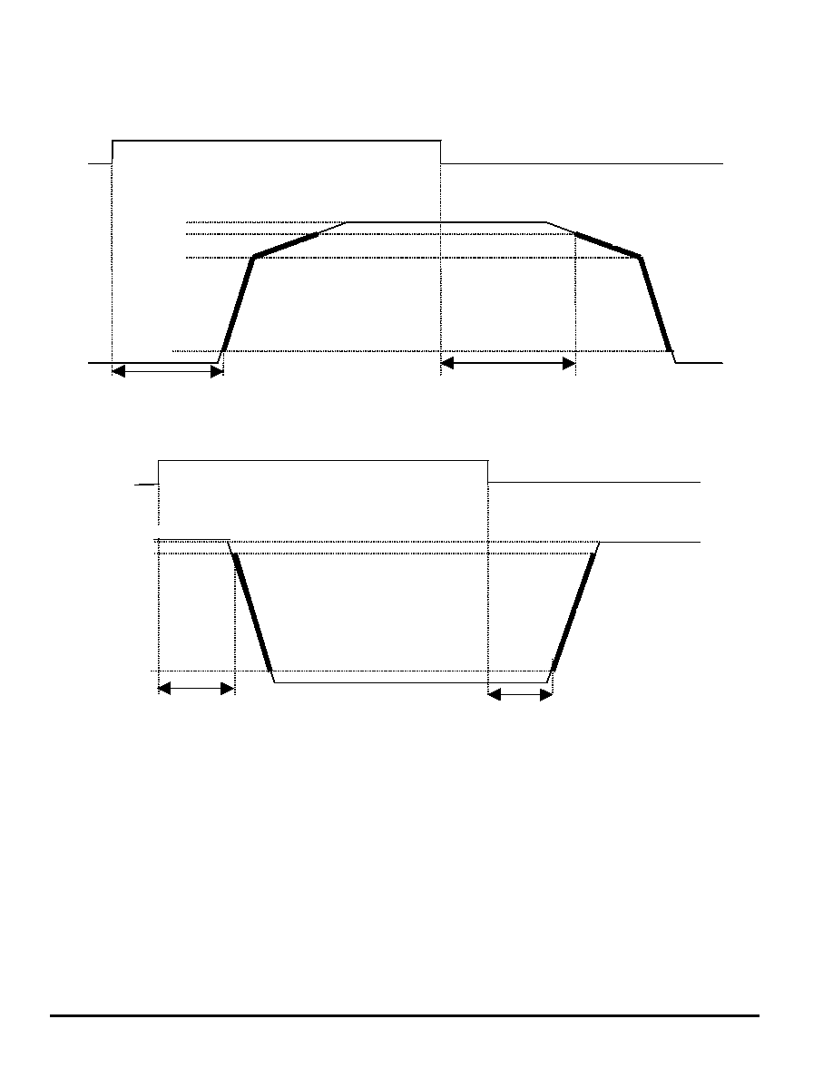
High-side output rise and fall fast slew rates measured across a 5.0
resistive load at high-side output = 0.5 V to V
PWR
-3.0 V (see
Figure 2
,
page 18). These parameters are guaranteed by process monitoring.
28.
High-side output rise and fall slow slew rates measured across a 5.0
resistive load at high-side output = 0.5 V to V
PWR
-3.0 V (see
Figure 2
, page 18). These parameters are guaranteed by process monitoring.
29.
High-side output turn-ON delay time measured from 50% of the rising IHS to 0.5 V of output OFF with R
L
= 27
resistive load (see
Figure 2
,
page 18).
30.
High-side output turn-OFF delay time measured from 50% of the falling IHS to V
PWR
-2.0 V of the output OFF with R
L
= 27
resistive load
(see
Figure 2
, page 18).
31.
Low-side output rise and fall slew rates measured across a 5.0
resistive load at low-side output = 10% to 90% (see
Figure 3
, page 18).
32.
Low-side output turn-ON delay time measured from 50% of the rising ILS to 90% of V
OUT
with R
L
= 27
resistive load (see
Figure 3
,
page 18).
33.
Low-side output turn-OFF delay time measured from 50% of the falling ILS to 10% of V
OUT
with R
L
= 27
resistive load (see
Figure 3
,
page 18). These parameters are guaranteed by process monitoring.
34.
Propagation time of Short Fault Disable Report Delay measured from rising edge of CS to output disabled, low-side = 5.0 V, and device
configured for low-side output overcurrent latchoff using CLOCCR.
35.
Watchdog timeout delay is measured from the rising edge of WAKE or RST from the sleep state to the HS[0:1] turn-ON with the outputs
driven OFF and the FSI floating. The accuracy of
t
WDTO
is maintained for all configured watchdog timeouts.
F
r
e
e
s
c
a
l
e
S
e
m
i
c
o
n
d
u
c
t
o
r
,
I
Freescale Semiconductor, Inc.
For More Information On This Product,
Go to: www.freescale.com
n
c
.
.
.
MOTOROLA ANALOG INTEGRATED CIRCUIT DEVICE DATA
33888
17
POWER OUTPUT TIMING (continued)
Peak Current Limit Timer
(Note 36)
t
PCT
40
70
100
ms
Direct Input Switching Frequency
(Note 37)
f
PWM
≠
125
≠
Hz
SPI INTERFACE TIMING
(Note 38)
Recommended Frequency of SPI Operation
Normal Mode
Extended Mode: V
DD
= 3.4 V; V
PWR
= 4.5 V, APNB Suffix Only
f
SPI
≠
≠
≠
≠
3.0
2.1
MHz
Required Low State Duration for RST
(Note 39)
t
WRST
≠
50
167
ns
Rising Edge of CS to Falling Edge of CS (Required Setup Time)
(Note 40)
t
CS
≠
≠
300
ns
Rising Edge of RST to Falling Edge of CS (Required Setup Time)
(Note 40)
t
ENBL
≠
≠
5.0
µs
Falling Edge of CS to Rising Edge of SCLK (Required Setup Time)
(Note 40)
t
LEAD
≠
50
167
ns
Required High State Duration of SCLK (Required Setup Time)
(Note 40)
t
WSCLKh
≠
≠
167
ns
Required Low State Duration of SCLK (Required Setup Time)
(Note 40)
t
WSCLKl
≠
≠
167
ns
Falling Edge of SCLK to Rising Edge of CS (Required Setup Time)
(Note 40)
t
LAG
≠
50
167
ns
SI to Falling Edge of SCLK (Required Setup Time)
(Note 40)
t
SI(SU)
≠
25
83
ns
Falling Edge of SCLK to SI (Required Hold Time)
(Note 40)
t
SI(HOLD)
≠
25
83
ns
SO Rise Time
C
L
= 200 pF
t
RSO
≠
25
50
ns
SO Fall Time
C
L
= 200 pF
t
FSO
≠
25
50
ns
SI, CS, SCLK, Incoming Signal Rise Time
(Note 41)
t
RSI
≠
≠
50
ns
SI, CS, SCLK, Incoming Signal Fall Time
(Note 41)
t
FSI
≠
≠
50
ns
Time from Falling Edge of CS to SO Low Impedance
(Note 42)
t
SO(EN)
≠
≠
145
ns
Time from Rising Edge of CS to SO High Impedance
(Note 43)
t
SO(DIS)
≠
65
145
ns
Time from Rising Edge of SCLK to SO Data Valid
(Note 44)
0.2 V
DD
SO 0.8 V
DD
, C
L
= 200 pF
t
VALID
≠
65
105
ns
Notes
36.
t
PCT
measured from the rising edge of CS to 90% of I
LIMPKHS[x,x]
when the peak current limit is enabled.
37.
This frequency is a typical value. Maximum switching frequencies are dictated by the turn-ON delay, turn-OFF delay, output rise and fall
times, and the maximum allowable junction temperature.
38.
Symmetrical 50% duty cycle SCLK clock period of 333 ns.
39.
RST
low duration measured with outputs enabled and going to OFF or disabled condition.
40.
Maximum setup time required for the 33888 is the minimum guaranteed time needed from the MCU.
41.
Rise and fall time of incoming SI, CS, and SCLK signals suggested for design consideration to prevent the occurrence of double pulsing.
42.
Time required for output status data to be available for use at SO. 1.0 k
pullup on CS.
43.
Time required for output status data to be terminated at SO. 1.0 k
pullup on CS.
44.
Time required to obtain valid data out from SO following the rise of SCLK.
DYNAMIC ELECTRICAL CHARACTERISTICS (continued)
Characteristics noted under conditions 6.0 V
V
PWR
27 V, 4.5 V
V
DD
5.5 V, -40
∞C
T
J
150
∞C unless otherwise noted. Typical
values noted reflect the approximate parameter mean at T
A
= 25
∞C under nominal conditions unless otherwise noted.
Characteristic
Symbol
Min
Typ
Max
Unit
F
r
e
e
s
c
a
l
e
S
e
m
i
c
o
n
d
u
c
t
o
r
,
I
Freescale Semiconductor, Inc.
For More Information On This Product,
Go to: www.freescale.com
n
c
.
.
.
33888
MOTOROLA ANALOG INTEGRATED CIRCUIT DEVICE DATA
18
Timing Diagrams
Figure 2. Output Slew Rates and Time Delays, High Side
Figure 3. Output Slew Rates and Time Delays, Low Side
VPWR
VPWR - 0.5V
VPWR - 3V
0.5V
Tdly(off)
SRr_fast
SRr_slow
SRf_fast
SRf_slow
Direct input or
spi bit
Tdly
(on)
V
PWR
V
PWR
-0.5 V
V
PWR
-3.0 V
t
DLY(OFF)
Direct Input or SPI Bit
SR
F_SLOW
SR
F_FAST
SR
R_SLOW
SR
R_FAST
t
DLY(ON)
0.5 V
Tdly(on)
VPWR
90%
10%
Tdly(off)
SRf
SRr
Direct input or SPI bit
t
DLY(ON)
t
DLY(OFF)
SR
R
SR
F
V
PWR
90%
10%
Direct Input or SPI Bit
F
r
e
e
s
c
a
l
e
S
e
m
i
c
o
n
d
u
c
t
o
r
,
I
Freescale Semiconductor, Inc.
For More Information On This Product,
Go to: www.freescale.com
n
c
.
.
.

MOTOROLA ANALOG INTEGRATED CIRCUIT DEVICE DATA
33888
19
SYSTEM/APPLICATION INFORMATION
INTRODUCTION
This 33888 is a single-package combination of a power die
with four discrete high-side MOSFETs and an integrated IC
control die consisting of eight low-side drivers with appropriate
control, protection, and diagnostic features. The high-side
drivers are useful for both internal and external vehicle lighting
applications as well as capable of driving inductive solenoid
loads. The low-side drivers are capable of controlling low-
current on/off type inductive loads, such as relays and
solenoids as well as LED indicators and small lamps (see
simplified application diagram,
page 2
). The device is useful in
body control, instrumentation, and other high-power switching
applications and systems.
The 33888 is available in two packages: a power-enhanced
12 x 12 nonleaded Power QFN package with exposed tabs and
a 64-lead Power QFP plastic package.
Both packages are
intended to be soldered directly onto the printed circuit board.
The 33888 differs from the 33888A as explained in
Table 1
,
page 2.
FUNCTIONAL DESCRIPTION
SPI Interface and Protocol Description
The SPI interface has full duplex, three-wire synchronous
data transfer and has four I/O lines associated with it: Serial
Clock (SCLK), Serial Input (SI), Serial Output (SO), and Chip
Select (
CS
).
The SI/SO terminals of the 33888 follow a first-in first-out
(D15/D0) protocol with both input and output words transferring
the most significant bit first. All inputs are compatible with 5.0 V
CMOS logic levels. During SPI output control, a logic [0] in a
message word will result in the designated output being turned
off. Similarly, a logic [1] will turn on a corresponding output.
The SPI lines perform the following functions:
Serial Clock (SCLK)
The SCLK terminal clocks the internal shift registers of the
33888. The serial input (SI) terminal accepts data into the input
shift register on the falling edge of the SCLK signal while the
serial output terminal (SO) shifts data information out of the SO
line driver on the rising edge of the SCLK signal. It is important
that the SCLK terminal be in a logic [0] state whenever the chip
select (
CS
) makes any transition. For this reason, it is
recommended that the SCLK terminal be kept in a logic [0] state
as long as the device is not accessed (
CS
in logic [1] state).
SCLK has an active
internal pulldown, I
DWN
. When
CS
is
logic [1], signals at the SCLK and SI terminals are ignored and
SO is tri-stated (high impedance). (See
Figures 4
and
5
on
page 20
.)
Serial Interface (SI)
This is a serial interface (SI) command data input terminal.
Each SI bit is read on the falling edge of SCLK. A 16-bit stream
of serial data is required on the SI terminal, starting with D15 to
D0. The 12 outputs of the 33888 are configured and controlled
using the 3-bit addressing scheme and the 12 assigned data
bits designed into the 33888. SI has an active
internal pulldown,
I
DWN
.
Serial Output (SO)
The SO data terminal is a tri-stateable output from the shift
register. The SO terminal remains in a high-impedance state
until the
CS
terminal is put into a logic [0] state. The SO data
report the status of the outputs as well as provide the capability
to reflect the state of the direct inputs. The SO terminal changes
states on the rising edge of SCLK and reads out on the falling
edge of SCLK. When an output is ON or OFF and not faulted,
the corresponding SO bit, OD11:OD0, is a logic [0]. If the output
is faulted, the corresponding SO state is a logic [1]. SO
OD14:OD12 reflect the state of six various inputs (three at a
time) depending upon the reported state of the previously
written watchdog bit OD15.
Chip Select (
CS
)
The
CS
terminal enables communication with the master
microcontroller (MCU). When this terminal is in a logic [0] state,
the 33888 is capable of transferring information to and receiving
information from the MCU. The 33888 latches in data from the
input shift registers to the addressed registers on the rising
edge of
CS
. The 33888 transfers status information from the
power outputs to the shift registers on the falling edge of
CS
.
The output driver on the SO terminal is enabled when
CS
is
logic [0].
CS
is only transitioned from a logic [1] state to a
logic [0] state when SCLK is a logic [0].
CS
has an active
internal pullup, I
UP
.
The 33888 is capable of communicating directly with the
MCU via the 16-bit SPI protocol as described in the next
section.
F
r
e
e
s
c
a
l
e
S
e
m
i
c
o
n
d
u
c
t
o
r
,
I
Freescale Semiconductor, Inc.
For More Information On This Product,
Go to: www.freescale.com
n
c
.
.
.
33888
MOTOROLA ANALOG INTEGRATED CIRCUIT DEVICE DATA
20
Figure 4. Single 16-Bit Word SPI Communication
Figure 5. Multiple 16-Bit Word SPI Communication
Serial Input Communication
SPI communication is accomplished using 16-bit messages.
A message is transmitted by the MCU starting with the MSB,
D15, and ending with the LSB, D0 (refer to
Table 2
, page 21).
Each incoming command message on the SI terminal can be
interpreted using the following bit assignments: the first twelve
LSBs, D11:D0, control each of the twelve outputs; the next
three bits, D14:D12, determine the command mode; and the
MSB, D15, is the watchdog bit.
Multiple messages can be transmitted in succession to
accommodate those applications where daisy chaining is
desirable or to confirm transmitted data, as long as the
messages are all multiples of 16 bits. Any attempt made to latch
in a message that is not 16 bits will be ignored.
The 33888 has six registers that are used to configure the
device and control the state of the four high-side and eight
low-side outputs (
Table 3
, page 21). The registers are
addressed via D14:D12 of the incoming SPI word (
Table 2
,
page 21).
CSB
SI
SCLK
D15
D1
D2
D3
D4
D5
D6
D7
D8
D9
D14
D13
D12
D11
D10
OD12
D0
OD13
OD14
OD15
OD6
OD7
OD8
OD9
OD10
OD11
OD1
OD2
OD3
OD4
OD5
OD0
SO
1. RST is in a logic [1] state during the above operation.
2. D15:D0 relate to the most recent ordered entry of program data into the 33888.
3. OD15:OD0 relate to the first 16 bits of ordered fault and status data out of the 33888.
Notes
CS
CSB
SI
SCLK
D15
D1*
D2*
D13*
D14*
D15*
D0
D1
D14
D13
D2
D0*
OD13
OD14
OD15
D14
D15
OD0
OD1
OD2
D1
D2
D13
D0
SO
1. RST is a logic [1] state during the above operation.
2. D15:D0 relate to the most recent ordered entry of program data into the 33888.
3. D15*:D0* relate to the first 16 bits of ordered entry data out of the 33888.
Notes
4. OD15:OD0 relate to the first 16 bits of ordered fault and status data out of the 33888.
CS
F
r
e
e
s
c
a
l
e
S
e
m
i
c
o
n
d
u
c
t
o
r
,
I
Freescale Semiconductor, Inc.
For More Information On This Product,
Go to: www.freescale.com
n
c
.
.
.
MOTOROLA ANALOG INTEGRATED CIRCUIT DEVICE DATA
33888
21
.
Device Register Addressing
The following section describes the possible register
addresses and their impact on device operation.
Address 000--SPI Output Control Register (SOCR)
The SOCR register allows the MCU to control the outputs via
the SPI. Incoming message bits D3:D0 reflect the desired
states of high-side outputs HS3:HS0. Message bits D11:D4
reflect the desired state of low-side outputs LS11:LS4,
respectively.
Address 100--Direct Input Control Register (DICR)
The DICR register is used by the MCU to enable direct input
control of the outputs. For the outputs, a logic [0] on bits D11:D0
will enable the corresponding output for direct control. A
logic [1] on a D11:D0 bit will disable the output from direct
control.
Address 010--Logic Function Control Register (LFCR)
The LFCR register is used by the MCU to configure the
relationship between SOCR bits D11:D0 and the direct inputs
IHS[0:3] and ILS. While addressing this register (if the direct
inputs were enabled for direct control with the DICR), a logic [1]
on any or all of the D3:D0 bits will result in a Boolean AND of
the IHS[0:3] terminal(s) with its (their) corresponding D3:D0
message bit(s) when addressing the SOCR. A logic [1] on any
or all of the D11:D4 bits will result in a Boolean AND of the ILS
and the corresponding D11:D4 message bits when addressing
the SOCR. Similarly, a logic [0] on the D3:D0 bits will result in
a Boolean OR of the IHS[0:3] terminal(s) with their
corresponding message bits when addressing the SOCR
register, and the ILS will be Boolean ORed with message bits
D11:D4 when addressing the SOCR register (if ILS is enabled).
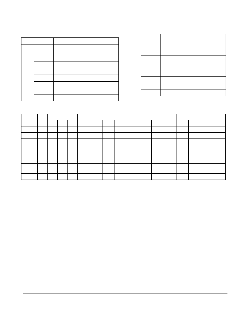
Table 2. SI Message Bit Assignment
Bit Sig
SI Msg Bit
Message Bit Description
MSB
D15
Watchdog in: toggled to satisfy watchdog
requirements.
D14:12
Register address bits.
D11
Used to configure Low-Side Output LS11.
D10
Used to configure Low-Side Output LS10.
D9
Used to configure Low-Side Output LS9.
D8
Used to configure Low-Side Output LS8.
D7
Used to configure Low-Side Output LS7.
D6
Used to configure Low-Side Output LS6.
Bit Sig
SI Msg Bit
Message Bit Description
D5
Used to configure Low-Side Output LS5
(Watchdog timeout MSB during WDCSCR
configuration).
D4
Used to configure Low-Side Output LS4
(Watchdog timeout LSB during WDCSCR
configuration).
D3
Used to configure High-Side Output HS3.
D2
Used to configure High-Side Output HS2.
D1
Used to configure High-Side Output HS1.
LSB
D0
Used to configure High-Side Output HS0.
Table 2. SI Message Bit Assignment (continued)
Table 3. Serial Input Address and Configuration Bit Map
SI
Register
WD
Address
Low-Side
High-Side
D15
D14
D13
D12
D11
D10
D9
D8
D7
D6
D5
D4
D3
D2
D1
D0
SOCR
x
0
0
0
LS11
LS10
LS9
LS8
LS7
LS6
LS5
LS4
HS3
HS2
HS1
HS0
DICR
x
1
0
0
PWB11 PWB10 PWB9 PWB8 PWB7 PWB6 PWB5 PWB4 PWB3 PWB2
PWB1
PWB0
LFCR
x
0
1
0
A/OB11 A/OB10 A/OB9 A/OB8 A/OB7 A/OB6 A/OB5 A/OB4 A/OB3 A/OB2 A/OB1 A/OB0
WDCSCR
x
1
1
0
NA
NA
NA
NA
NA
NA
WDH
WDL
CS3
CS2
CS1
CS0
OLCR
x
0
0
1
OL11
OL10
OL9
OL8
OL7
OL6
OL5
OL4
OLB3
OLB2
OLB1
OLB0
CLOCCR
x
1
0
1
OC11
OC10
OC9
OC8
OC7
OC6
OC5
OC4
ILIM3
ILIM2
ILIM1
ILIM0
NOT
USED
x
0
1
1
≠
≠
≠
≠
≠
≠
≠
≠
≠
≠
≠
≠
TEST
x
1
1
1
≠
≠
≠
≠
≠
≠
≠
≠
ILIMPK
WD
ILIM
OT
x=Don't care.
NA=Not applicable.
F
r
e
e
s
c
a
l
e
S
e
m
i
c
o
n
d
u
c
t
o
r
,
I
Freescale Semiconductor, Inc.
For More Information On This Product,
Go to: www.freescale.com
n
c
.
.
.

33888
MOTOROLA ANALOG INTEGRATED CIRCUIT DEVICE DATA
22
Address 110--Watchdog and Current Sense Configuration
Register (WDCSCR)
The WDCSCR register is used by the MCU to configure the
watchdog timeout and the CSNS0-1 and CSNS2-3 terminals.
The watchdog timeout is configured using bits D4 and D5. The
state of D4 and D5 determine the divided value of the WDTO.
For example, if D5 and D4 are logic [0] and logic [0],
respectively, then the WDTO will be in the default state as
specified in
Table 3
, page 21. A D5 and a D4 of logic [0] and
logic [1] will result in a watchdog timeout of WDTO
˜ 2.
Similarly, a D5 and a D4 of logic [1] and logic [0] result in a
watchdog timeout of WDTO
˜ 4, and a D5 and a D4 of logic [1]
and logic [1] result in a watchdog timeout of WDTO
˜ 8. Note
that when D5 and D4 bits are programmed for the desired
watchdog timeout period, the WD bit (D15) should be toggled
as well to ensure that the new timeout period is programmed at
the beginning of a new count sequence.
CSNS0-1 is the current sense output for the HS0 and HS1
outputs. Similarly, the CSNS2-3 terminal is the current sense
output for the HS2 and HS3 outputs. In this mode, a logic [1] on
any or all of the message bits that control the high-side outputs
will result in the sensed current from the corresponding output
being directed out of the appropriate CSNS output. For
example, if D1 and D0 are both logic [1], then the sensed
current from HS0 and HS1 will be summed into the CSNS0-1.
If D2 is logic [1] and D3 is logic [0], then only the sensed current
from HS2 will be directed out of CSNS2-3.
Address 001--Open Load Configuration Register (OLCR)
The OLCR register allows the MCU to configure each of the
outputs for open load fault detection. While in this mode, a
logic [1] on any of the D3:D0 message bits will disable the
corresponding outputs' circuitry that allows the device to detect
open load faults while the output is OFF. For the low-side
drivers, a logic [1] on any of the D11:D4 bits will enable the
open load detection circuitry. This feature allows the MCU to
minimize load current in some applications and may be useful
to diagnose output shorts to battery (for HS).
Address 101--Current Limit Overcurrent Configuration
Register (CLOCCR)
The CLOCCR register allows the MCU to individually
override the peak current limit levels for each of the high-side
outputs. A logic [1] on any or all of the D3:D0 bit(s) results in the
corresponding HS3:HS0 output terminals to current limit at the
sustain current limit level. This register also allows the MCU to
enable or disable the overcurrent shutdown of the low-side
output terminals. A logic [1] on any or all of the D11:D4
message bit(s) will result in the corresponding LS11:LS4
terminals latching off if the current exceeds I
LIM
after a timeout
of t
DLY(
FS
)
.
Address 011--Not Used
Not currently used.
Address 111--TEST
The TEST register is reserved for test and is not accessible
via SPI during normal operation.
Serial Output Communication (Devise Status
Return Data)
When the
CS
terminal is pulled low, the output status register
for each output is loaded into the output register and the fault
data is clocked out MSB (OD15) first as the new message data
is clocked into the SI terminal.
OD15 reflects the state of the watchdog bit (D15) that was
addressed during the prior SOCR communication (refer to
Table 4
, page 23). If bit OD15 is logic [0], then the three MSBs
OD14:OD12 will reflect the logic states of the IHS0, IHS1, and
FSI terminals, respectively. If bit OD15 is logic [1], then the
same three MSB bits will reflect the logic states of the IHS2,
IHS3, and WAKE terminals. The next twelve bits clocked out of
SO following a low transition of the
CS
terminal (OD11:OD0)
will reflect the state of each output, with a logic [1] in any of the
bits indicating that the respective output experienced a fault
condition prior to the
CS
transition. Any bits clocked out of the
SO terminal after the first 16 will be representative of the initial
message bits that were clocked into the SI terminal since the
CS
terminal first transitioned to a logic [0]. This feature is useful for
daisy chaining devices as well as message verification.
Following a
CS
transition logic [0] to logic [1], the device
determines if the message was of a valid length (a valid
message length is one that is a multiple of 16 bits) and if so,
latches the data into the appropriate registers. At this time, the
SO terminal is tri-stated and the fault status register is now able
to accept new fault status information.
F
r
e
e
s
c
a
l
e
S
e
m
i
c
o
n
d
u
c
t
o
r
,
I
Freescale Semiconductor, Inc.
For More Information On This Product,
Go to: www.freescale.com
n
c
.
.
.
MOTOROLA ANALOG INTEGRATED CIRCUIT DEVICE DATA
33888
23
MODES OF OPERATION
Watchdog and Fail-Safe Operation
The watchdog is enabled and a timeout is started when the
WAKE or
RST
transitions from logic [0] to logic [1]. The WAKE
input is capable of being pulled up to V
PWR
with a series limiting
resistance that limits the internal clamp current. The timeout is
a multiple of an internal oscillator. As long as the WDIN terminal
or the WD bit (D15) of an incoming SPI message is toggled
within the minimum watchdog timeout, WDTO (or a divided
value configured during a WDCSCR message), then the device
will operate normally. If the watchdog timeout occurs before the
WD bit or the WDIN terminal is toggled, then the device will
revert to a Fail-Safe mode until the device is reinitialized (if the
FSI terminal is left disconnected).
During Fail-Safe mode, all outputs will be OFF except for
HS0 and HS2, which will be driven ON regardless of the state
of the various direct inputs and modes (
Table 5
). The device
can be brought out of the Fail-Safe mode by transitioning the
WAKE and
RST
terminals from logic [1] to logic [0]. In the event
the WAKE terminal was not transitioned to a logic [1] during
normal operation and the watchdog times out, then the device
can be brought out of fail-safe by bringing the
RST
to a logic [0].
If the FSI terminal is tied to GND, then the watchdog, and
therefore fail-safe operation, will be disabled.
Table 4. Serial Output Bit Assignment
Bit Sig
SO
Msg Bit
Message Bit Description
MSB
OD15
Reflects the state of the Watchdog bit from the
previously clocked-in message.
OD14
If OD15 is logic [0], then this bit will reflect the state
of the direct input IHS0. If OD15 is logic [1], then this
bit will reflect the state of IHS2.
OD13
If OD15 is logic [0], then this bit will reflect the state
of the direct input IHS1. If OD15 is logic [1], then this
bit will reflect the state of IHS3.
OD12
If OD15 is logic [0], then this bit will reflect the state
of the input FSI. If OD15 is logic [1], then this bit will
reflect the state of the input WAKE.
OD11
Reports the absence or presence of a fault on LS11.
OD10
Reports the absence or presence of a fault on LS10.
Bit Sig
SO
Msg Bit
Message Bit Description
OD9
Reports the absence or presence of a fault on LS9.
OD8
Reports the absence or presence of a fault on LS8.
OD7
Reports the absence or presence of a fault on LS7.
OD6
Reports the absence or presence of a fault on LS6.
OD5
Reports the absence or presence of a fault on LS5.
OD4
Reports the absence or presence of a fault on LS4.
OD3
Reports the absence or presence of a fault on HS3.
OD2
Reports the absence or presence of a fault on HS2.
OD1
Reports the absence or presence of a fault on HS1.
LSB
OD0
Reports the absence or presence of a fault on HS0.
Table 4. Serial Output Bit Assignment (continued)
Table 5. Fail-Safe Operation and Transitions
to Other 33888 Modes
WAKE RST WDTO HS0 HS2
LS[4:11],
HS[1,3]
Comments
0
0
x
OFF OFF
OFF
Device in Sleep mode.
1
0
NO
OFF OFF
OFF
All outputs are OFF.
When RST transitions
to logic [1], device is in
default.
1
0
YES
ON
ON
OFF
Fail-Safe mode.
Device reset into
Default mode by
transitioning WAKE to
logic [0].
0
1
NO
S
S
S
Device in Normal
operating mode.
0
1
YES
ON
ON
OFF
Fail-Safe mode.
Device reset into
Default mode by
transitioning RST to
logic [0].
1
1
NO
S
S
S
Device in Normal
operating mode.
1
1
YES
ON
ON
OFF
Fail-Safe mode.
Device reset into
Default mode by
transitioning RST and
WAKE to logic [0].
Assumptions: Normal operating voltage and junction temperatures,
FSI terminal floating.
x=Don't care.
S=State determined by SPI and/or direct input configurations.
F
r
e
e
s
c
a
l
e
S
e
m
i
c
o
n
d
u
c
t
o
r
,
I
Freescale Semiconductor, Inc.
For More Information On This Product,
Go to: www.freescale.com
n
c
.
.
.

33888
MOTOROLA ANALOG INTEGRATED CIRCUIT DEVICE DATA
24
Default Mode
The default mode describes the state of the device after first
applying V
PWR
voltage or a reset transition from logic [0] to
logic [1] prior to SPI communication. In the default mode, all
outputs will be off (assuming that the direct inputs ILS and
IHS[0:3] and the WAKE terminal are at logic [0]). All of the
specific terminal functions will operate as though all of the
addressable configuration register bits were set to logic [0]. This
means, for example, that all of the low-side outputs will be
controllable by the ILS terminal, and that all high-side outputs
will be controllable via their respective IHS terminals. During the
default mode, all high-side drivers will default with open load
detection enabled. All low-side drivers will default with open
load detection disabled. This mode allows limited control of the
33888 with the direct inputs in the absence of a
n
SPI.
Returning the device to the default state after a period of
normal operation, followed by the removal of the V
PWR
voltage,
requires that the
RST
input be held at a logic [0] state until V
PWR
falls to a level below 2.0 V. If the
RST
and V
DD
input levels are
normal, then failure to allow V
PWR
to fall below 2.0 V will result
in an internal bias circuit clamping the V
PWR
terminal to
approximately 3.5 V. Once V
PWR
falls below 2.0 V, the
RST
can
be returned to 5.0 V without re-enabling the bias circuit.
Fault Logic Requirements
The 33888 indicates all of the following faults as they occur:
∑ Overtemperature Fault
∑ Overvoltage Fault
∑ Open Load Fault
∑ Overcurrent Fault
With the exception of the overvoltage, these faults are output
specific. The overvoltage fault is a global fault. The overcurrent
fault is only reported for the low-side outputs.
The 33888 low-side outputs incorporate an internal fault
filter, t
DLY(
FS
)
. The fault timer filters noise and switching
transients for overcurrent faults when the output is ON and
open load faults when the output is OFF. All faults are latched
and indicated by a logic [1] for each output in the 33888 status
word (
Table 4
, page 23). If the fault is removed, the status bit for
the faulted output will be cleared by a rising edge on
CS
.
The
FS
terminal is driven to a logic [0] when a fault exists on
any of the outputs.
FS
provides real time monitoring of the
overvoltage fault. For the high-side outputs,
FS
provides real
time monitoring of the open load and overtemperature. For the
low-side outputs, the
FS
is latched to a logic [0] for open load,
overtemperature, and overcurrent faults. The latch is cleared by
toggling the state of the faulted output or by bringing
RST
low.
Overtemperature Fault
The 33888 incorporates overtemperature detection and
shutdown circuitry into each individual output structure.
Overtemperature detection occurs when an output is in the ON
state. When an output is shut down due to an overtemperature
condition, no other output is affected. The output experiencing
the fault is shut down to protect itself from damage. A fault bit is
loaded into the status register if the overtemperature condition
is removed, and the fault bit is cleared upon the rising edge of
CS
.
For the low-side outputs, the faulted output is latched OFF
during an overtemperature condition. If the temperature falls
below the recovery level, T
LIM(HYS)
, then the output can be
turned back ON only after the output has first been commanded
OFF either through the SPI or the ILS, depending on the logic
configuration.
For the high-side output(s), an overtemperature condition will
result in the output(s) turning OFF until the temperature falls
below the T
LIM(HYS)
. This cycle will continue indefinitely until
action is taken by the MCU to shut the output(s) OFF.
Overvoltage Fault
The 33888 shuts down all outputs during an overvoltage
condition on the V
PWR
terminal. The outputs remain in the OFF
state until the overvoltage condition is removed. Fault status for
all outputs is latched into the status register. Following an
overvoltage condition, the next write cycle sent by the SO
terminal of the 33888 is logic [1] on OD11:OD0, indicating all
outputs have shut down. If the overvoltage condition is
removed, the status register can be cleared by a rising edge on
CS
.
Open Load Fault
The 33888 incorporates open load detection circuitry on
every output. A high-side or low-side output open load fault is
detected and reported as a fault condition when the
corresponding output is disabled (OFF) if it was configured for
open load detection by setting the appropriate bit to logic [0]
(HS3:HS0) or logic [1] (LS11:LS4) in the OLFCR register
(
Figure 6
, page 25).
The high-side open load fault is detected and latched into the
status register after the internal gate voltage is pulled low
enough to turn off the output. If the open load fault is removed
or if the faulted output is commanded ON, the status register
can be cleared by a rising edge on
CS
. Note that the device
default state will enable the high-side open load detection and
disable the low-side open load detection circuits, respectively.
F
r
e
e
s
c
a
l
e
S
e
m
i
c
o
n
d
u
c
t
o
r
,
I
Freescale Semiconductor, Inc.
For More Information On This Product,
Go to: www.freescale.com
n
c
.
.
.
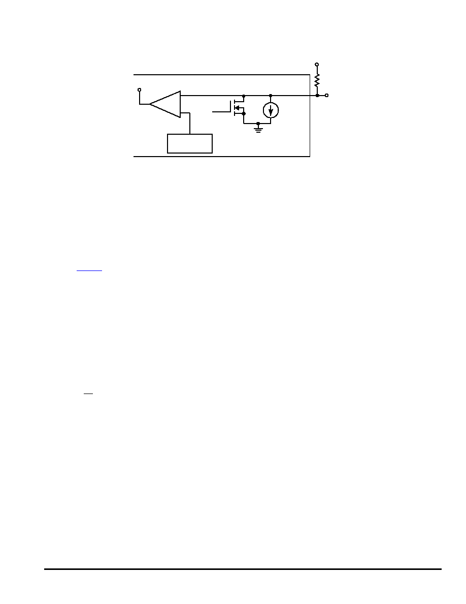
MOTOROLA ANALOG INTEGRATED CIRCUIT DEVICE DATA
33888
25
Figure 6. Low-Side Output OFF Open Load Detection
Overcurrent Fault Requirements: Low-Side Output
An overcurrent condition is defined as any current value
greater than I
LIM
(500 mA minimum value for LS5, LS7, LS9,
LS11, and 800 mA minimum value for LS4, LS6, LS8, LS10).
The status of the corresponding bit in the CLOCCR register
determines whether a specific output shuts down or continues
to operate in an analog current limited mode until either the
overcurrent condition is removed or the thermal shutdown limit
is reached (
Figure 7
, page 26). If the overcurrent shutdown
mode is disabled, the fault reporting is disabled as well.
For the low-side output of interest, if a D11:D4 bit was set to
a logic [1] in the OLCR register, the overcurrent protection
shutdown circuitry will be enabled for that output. When a low-
side output is commanded ON either from the SPI or the ILS
terminal, the drain of the low-side driver will be monitored for a
voltage greater than the fault detection threshold (3.0 V typical).
If the drain voltage exceeds this threshold, a timer will start and
the output will be turned off and a fault latched in the status
register after the timeout expires. The faulted output can be
retried only by commanding the output OFF and back ON either
through the SPI or the ILS terminal, depending on the logic
configuration. If the fault is gone, the retried output will return to
normal operation and the status register can be cleared on a
rising edge of
CS
. If the fault remains, the retried output will
latch off after the fault timer expires and the fault bit will remain
set in the status register.
For the low-side output of interest, if a D11:D4 bit was set to
a logic [0] in the OLCR register, the output experiencing an
overcurrent condition is not disabled until an overtemperature
fault threshold has been reached. The specific output goes into
an analog current limit mode of operation, I
LIM
. The 33888 uses
overtemperature shutdown to protect all outputs in this mode of
operation. If the overcurrent condition is removed before the
output has reached its overtemperature limit, the output will
function as if no fault has occurred.
Note that each pair of low-side drivers, LS4:LS5, LS6:LS7,
LS8:LS9, and LS10:LS11, consists of a 500 mA and a 800 mA
output. Each pair of outputs shares ground bondwires. The
bondwires are not rated to handle both outputs in current limit
mode simultaneously.
Overcurrent Fault Requirements: High-Side Output
For the high-side output of interest, the output current is
limited to one of four levels depending on the type of high-side
output, the amount of time that has elapsed since the output
was switched on, and the state of the CLOCCR register.
Assuming that bits D3:D0 of the CLOCCR register are at
logic [0], the current limit levels of the outputs will be initially at
their peak levels as specified by the I
LIM(PK)HS[0:3]
. After the
high-side output is switched on, the peak current timer starts.
After a period of time t
PCT
, the current limit level changes to the
sustain levels I
LIMSUSHS[x,x]
.
For the high-side output of interest, if a D3:D0 bit of the
CLOCCR is at logic [1], then the assigned output will only
current limit at the sustain level specified by I
LIMSUSHS[x,x]
.
Current is limited until the overtemperature circuitry shuts
OFF the device. The device turns ON automatically when the
temperature fails below the T
LIM(HYS)
. This cycle continues
indefinitely until action is taken by the master to shut the
output(s) OFF.
Reverse Battery Requirements
The low-side and high-side outputs survive the application of
reverse battery as low as -16 V.
Ground Disconnect Protection
In the event that the 33888 ground is disconnected from load
ground, the device protects itself and safely turns OFF the
outputs, regardless of the state of the output at the time of
disconnection.
OUTPUT
V
THRES
MOSFET
R
L
V
PWR
LOW = Logic 0
50 mA
V
OFD(THRES)LS
2.0 V≠4.0 V
≠
+
33888
V
PWR
R
L
OUT
F
r
e
e
s
c
a
l
e
S
e
m
i
c
o
n
d
u
c
t
o
r
,
I
Freescale Semiconductor, Inc.
For More Information On This Product,
Go to: www.freescale.com
n
c
.
.
.
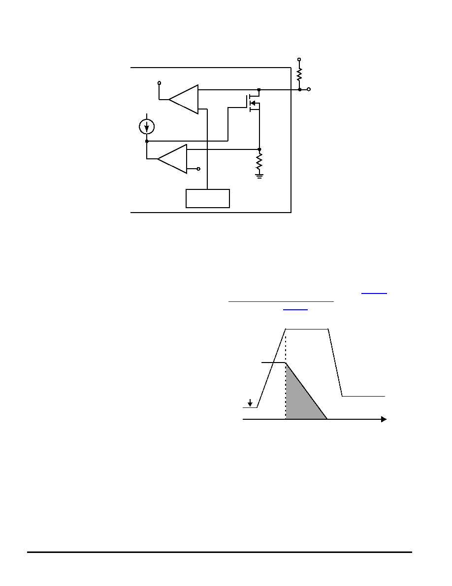
33888
MOTOROLA ANALOG INTEGRATED CIRCUIT DEVICE DATA
26
Figure 7. Low-Side Short Circuit Detection and Analog Current Limit
Undervoltage Shutdown Requirements
All outputs turn off at some battery voltage below 6.0 V; For
the A version, the low side shutdown at a lower value,
V
PWRUV
.
however, as long as the level stays above 5.0 V, the internal
logic states within the device are designed to be sustained. This
ensures that when the battery level then rises above 6.0 V, the
device will return to the state that it was in prior to the excursion
between 5.0 V and 6.0 V (assuming that there was no SPI
communication or direct input changes during the event). If the
battery voltage falls to a level below 5.0 V, then the internal
logic is reinitialized and the device is then in the default state
upon the return of levels in excess of 6.0 V.
Output Voltage Clamping
Each output has an internal clamp to provide protection and
dissipate the energy stored in inductive loads. Each clamp
independently limits the drain-to-source voltage to the range
specified in the Power Outputs section of the
STATIC
ELECTRICAL CHARACTERISTICS
table beginning on
page 12. Also see
Figure 8
.
Figure 8. Low-Side Output Voltage Clamping
V
THRES
V
OFD(THRES)LS
2.0 V≠4.0 V
Analog
Digital
≠
+
≠
+
HIGH = Fault
MOSFET ON
V
REF
V
PWR
R
L
OUT
33888
V
PWR
Time
GND
Current
Area (I
A
)
Clamp Energy
(E
J
= I
A
x V
CL
x t)
Drain Voltage
Drain-Source
Clamp Voltage
(V
CL
= 53 V)
Drain-Source
ON Voltage
(V
DS(ON)
)
Drain Current
(I
D
= 0.5 A)
F
r
e
e
s
c
a
l
e
S
e
m
i
c
o
n
d
u
c
t
o
r
,
I
Freescale Semiconductor, Inc.
For More Information On This Product,
Go to: www.freescale.com
n
c
.
.
.
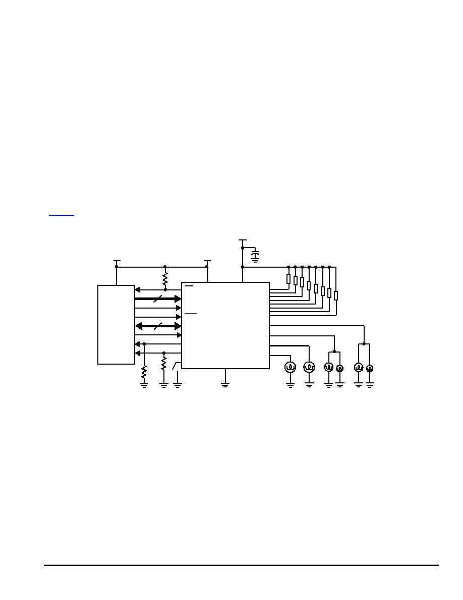
MOTOROLA ANALOG INTEGRATED CIRCUIT DEVICE DATA
33888
27
PACKAGE INFORMATION
Soldering Information
The 33888 is packaged in a surface mount power package
intended to be soldered directly onto the printed circuit board.
The device was qualified in accordance with JEDEC
standards JESD22-A113-B and J-STD-020A. The
recommended reflow conditions are as follows:
∑ Convection: 225∞C +5.0∞C/-0∞C
∑ Vapor Phase Reflow (VPR): 215∞C to 219∞C
∑ Infrared (IR)/Convection: 225∞C +5.0∞C/-0∞C
The maximum peak temperature during the soldering
process should not exceed 230∞C. The time at maximum
temperature should range from 10 seconds to 40 seconds
maximum.
APPLICATIONS
Typical Application
Figure 9
shows a typical application for the 33888.
Figure 9. 33888 Typical Application Diagram
RST
V
DD
FS
WDIN
8 x Relay or LED
V
DD
V
PWR
V
PWR
MCU
65 W
Loads
+5.0 V
+5.0 V
4
4
IHS0:IHS3
33888
GND
SPI
CSNS2-3
CSNS0-1
ILS
FSI
65 W
21 W 5.0 W
21 W 5.0 W
10 k
8 x 0.5
40 m
40 m
10 m
10 m
A/D
A/D
R
C1
R
C2
F
r
e
e
s
c
a
l
e
S
e
m
i
c
o
n
d
u
c
t
o
r
,
I
Freescale Semiconductor, Inc.
For More Information On This Product,
Go to: www.freescale.com
n
c
.
.
.
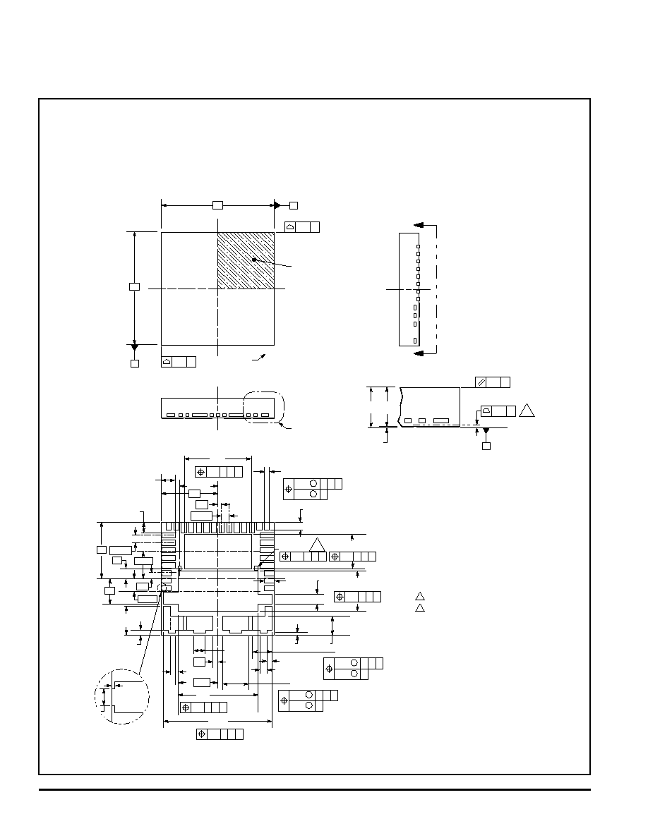
33888
MOTOROLA ANALOG INTEGRATED CIRCUIT DEVICE DATA
28
PACKAGE DIMENSIONS
30X
A
12
12
B
1
14
16
23
25
28
29
36
2X
C
0.1
PIN NUMBER
REFERENCE ONLY
PIN 1
INDEX AREA
M
M
DETAIL G
2.2 2.20
0.05
2.0 1.95
0.00
C
0.1
C
0.05
C
SEATING PLANE
4
DETAIL G
VIEW M-M
(Bottom View)
(Top View)
A
0.1
B C
11.7
11.3
A
0.1
B C
8.70
8.30
2X
3.75
0.5
(
2X
0.75)
(
2X
0.75)
(
2X
0.5)
(
2X
1.25)
M
0.1
C
M
0.05
C
A B
2X
2.95
2.55
M
0.1
C
M
0.05
C
A B
2X
2.2
1.8
4X
0.2
0.0
6X
1.25
1.00
4X
2.0
1.5
4.45
4.05
1.45
1.05
A
0.1
B C
A
0.1
B C
3.85
3.45
A
0.1
B C
0.4±0.2
2 PLACES
X
0.5±0.2
0.90
0.65
M
0.1
C
M
0.05
C
A B
30X
2X
0.62
0.48
10X
1.60
1.35
10X
1.20
0.95
5
A
0.1
B C
7.3
6.9
4.05
13X
0.8
0.4
6
6
1
0.6
2.875
7X
0.8
(0.25)
(0.05)
1.625
3
2X
2.8
2.3
(0.3)
1
36
29
28
27
26
25
24
15
23
16
14
4X
C
0.1
CASE 1438-06
ISSUE E
NOTES:
1.
2.
3.
4.
5.
6.
ALL DIMENSIONS ARE IN MILLIMETERS.
DIMENSIONING AND TOLERANCING PER ASME
Y14.5M, 1994.
THE COMPLETE JEDEC DESIGNATOR FOR
THIS PACKAGE IS: HF-PQFP-N.
COPLANARITY APPLIES TO LEADS AND
CORNER LEADS.
METAL PADS CONNECTED TO THE GND.
MINIMUM METAL GAP SHOULD BE 0.25MM.
PNB SUFFIX
APNB SUFFIX
36-TERMINAL PQFN
NONLEADED PACKAGE
CASE 1438-06
ISSUE E
F
r
e
e
s
c
a
l
e
S
e
m
i
c
o
n
d
u
c
t
o
r
,
I
Freescale Semiconductor, Inc.
For More Information On This Product,
Go to: www.freescale.com
n
c
.
.
.
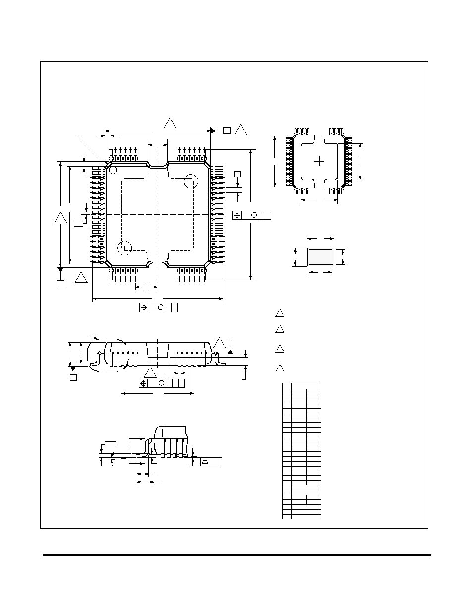
MOTOROLA ANALOG INTEGRATED CIRCUIT DEVICE DATA
33888
29
C
A4
A
64X
SEATING
PLANE
H
A2
b
M
aaa
C A B
E3
DATUM
PLANE
DETAIL Y
5
3
NOTES:
1. DIMENSIONS ARE IN MILLIMETERS.
2. INTERPRET DIMENSIONS AND TOLERANCES
PER ASME Y14.5M, 1994.
3. DATUM PLANE -H- IS LOCATED AT BOTTOM OF
LEAD AND IS COINCIDENT WITH THE LEAD
WHERE THE LEAD EXITS THE PLASTIC BODY AT
THE BOTTOM OF THE PARTING LINE.
4. DIMENSIONS "D1" AND "E1" DO NOT INCLUDE
MOLD PROTRUSION. ALLOWABLE PROTRUSION
IS 0.15 PER SIDE. DIMENSION "D1" AND "E1" DO
INCLUDE MOLD MISMATCH AND ARE
DETERMINED AT DATUM PLANE -H-.
5. DIMENSION "b" DOES NOT INCLUDE DAMBAR
PROTRUSION. ALLOWABLE DAMBAR
PROTRUSION SHALL BE 0.127 TOTAL IN EXCESS
OF THE "b" DIMENSION AT MAXIMUM MATERIAL
CONDITION.
6. DATUMS -A- AND -B- TO BE DETERMINED AT
DATUM PLANE -H-.
DIM
MIN
MAX
MILLIMETERS
A
---
3.15
A1
---
0.25
A2
2.5
2.9
A3
0
0.1
A4
D
D1
D2
12.5
12.9
D3
9.3
9.7
D4
13.4
13.6
E
E1
E2
E3
L
0.8
1.1
b
b1
0.22
0.33
c
c1
e
0.65 BSC
e1
h
---
0.8
aaa
0.12
0∞
bbb
0.2
ccc
0.1
0.8
1
16.95
17.45
13.9
14.1
13.9
14.1
2.35
2.65
9.3
9.7
16.95
17.45
0.22
0.38
0.23
0.32
0.23
0.29
2.925 BSC
7∞
E1
64
20
1
53
D
2X
52
33
21
32
e
M
bbb
C A
58X
e1
4X
E
M
bbb
C B
E2
e/2
2X
D1
D2
h
h
A
4
4
6
6
B
PIN ONE
ID
D3
D4
E3
BOTTOM VIEW
b1
b
SECTION W-W
c
c1
A1
(1.6)
L
0.35
A3
DETAIL Y
W
W
ccc
GAUGE
PLANE
FB SUFFIX
64-TERMINAL PQFP
PLASTIC PACKAGE
CASE 1315-03
ISSUE B
F
r
e
e
s
c
a
l
e
S
e
m
i
c
o
n
d
u
c
t
o
r
,
I
Freescale Semiconductor, Inc.
For More Information On This Product,
Go to: www.freescale.com
n
c
.
.
.

33888
MOTOROLA ANALOG INTEGRATED CIRCUIT DEVICE DATA
30
NOTES
F
r
e
e
s
c
a
l
e
S
e
m
i
c
o
n
d
u
c
t
o
r
,
I
Freescale Semiconductor, Inc.
For More Information On This Product,
Go to: www.freescale.com
n
c
.
.
.

MOTOROLA ANALOG INTEGRATED CIRCUIT DEVICE DATA
33888
31
NOTES
F
r
e
e
s
c
a
l
e
S
e
m
i
c
o
n
d
u
c
t
o
r
,
I
Freescale Semiconductor, Inc.
For More Information On This Product,
Go to: www.freescale.com
n
c
.
.
.

HOW TO REACH US:
USA/EUROPE/LOCATIONS NOT LISTED:
JAPAN: Motorola Japan Ltd.; SPS, Technical Information Center
Motorola Literature Distribution
3-20-1 Minami-Azabu. Minato-ku, Tokyo 106-8573, Japan
P.O. Box 5405, Denver, Colorado 80217
81-3-3440-3569
1-800-521-6274 or 480-768-2130
ASIA/PACIFIC: Motorola Semiconductors H.K. Ltd.; Silicon Harbour Centre
2 Dai King Street, Tai Po Industrial Estate, Tai Po, N.T., Hong Kong
852-26668334
HOME PAGE: http://motorola.com/semiconductors
MC33888
Information in this document is provided solely to enable system and software implementers to use Motorola products. There are no express or implied
copyright licenses granted hereunder to design or fabricate any integrated circuits or integrated circuits based on the information in this document.
Motorola reserves the right to make changes without further notice to any products herein. Motorola makes no warranty, representation or guarantee
regarding the suitability of its products for any particular purpose, nor does Motorola assume any liability arising out of the application or use of any product
or circuit, and specifically disclaims any and all liability, including without limitation consequential or incidental damages. "Typical" parameters which may be
provided in Motorola data sheets and/or specifications can and do vary in different applications and actual performance may vary over time. All operating
parameters, including "Typicals" must be validated for each customer application by customer's technical experts. Motorola does not convey any license
under its patent rights nor the rights of others. Motorola products are not designed, intended, or authorized for use as components in systems intended for
surgical implant into the body, or other applications intended to support or sustain life, or for any other application in which the failure of the Motorola product
could create a situation where personal injury or death may occur. Should Buyer purchase or use Motorola products for any such unintended or
unauthorized application, Buyer shall indemnify and hold Motorola and its officers, employees, subsidiaries, affiliates, and distributors harmless against all
claims, costs, damages, and expenses, and reasonable attorney fees arising out of, directly or indirectly, any claim of personal injury or death associated
with such unintended or unauthorized use, even if such claim alleges that Motorola was negligent regarding the design or manufacture of the part.
MOTOROLA and the Stylized M Logo are registered in the US Patent and Trademark Office. All other product or service names are the property of their
respective owners.
© Motorola, Inc. 2004
F
r
e
e
s
c
a
l
e
S
e
m
i
c
o
n
d
u
c
t
o
r
,
I
Freescale Semiconductor, Inc.
For More Information On This Product,
Go to: www.freescale.com
n
c
.
.
.