 | –≠–ª–µ–∫—Ç—Ä–æ–Ω–Ω—ã–π –∫–æ–º–ø–æ–Ω–µ–Ω—Ç: SG3526 | –°–∫–∞—á–∞—Ç—å:  PDF PDF  ZIP ZIP |

Device
Operating
Temperature Range
Package
SG3526
SEMICONDUCTOR
TECHNICAL DATA
PULSE WIDTH MODULATION
CONTROL CIRCUIT
ORDERING INFORMATION
SG3526N
TJ = 0
∞
to +125
∞
C
Plastic DIP
PIN CONNECTIONS
Order this document by SG3526/D
N SUFFIX
PLASTIC PACKAGE
CASE 707
18
1
(Top View)
+Error
Compensation
CSoft≠Start
≠CS
+CS
Shutdown
≠Error
Reset
RT
RDeadtime
Sync
Output A
Ground
Output B
VCC
Vref
VC
CT
1
2
3
4
5
6
7
8
12
13
14
15
16
17
18
9
11
10
1
MOTOROLA ANALOG IC DEVICE DATA
Pulse Width Modulation
Control Circuit
The SG3526 is a high performance pulse width modulator integrated
circuit intended for fixed frequency switching regulators and other power
control applications.
Functions included in this IC are a temperature compensated voltage
reference, sawtooth oscillator, error amplifier, pulse width modulator, pulse
metering and steering logic, and two high current totem pole outputs ideally
suited for driving the capacitance of power FETs at high speeds.
Additional protective features include soft start and undervoltage lockout,
digital current limiting, double pulse inhibit, adjustable dead time and a data
latch for single pulse metering. All digital control ports are TTL and B≠series
CMOS compatible. Active low logic design allows easy wired≠OR
connections for maximum flexibility. The versatility of this device enables
implementation in single≠ended or push≠pull switching regulators that are
transformerless or transformer coupled. The SG3526 is specified over a
junction temperature range of 0
∞
to +125
∞
C.
∑
8.0 V to 35 V Operation
∑
5.0 V
±
1% Trimmed Reference
∑
1.0 Hz to 400 kHz Oscillator Range
∑
Dual Source/Sink Current Outputs:
±
100 mA
∑
Digital Current Limiting
∑
Programmable Dead Time
∑
Undervoltage Lockout
∑
Single Pulse Metering
∑
Programmable Soft≠Start
∑
Wide Current Limit Common Mode Range
∑
Guaranteed 6 Unit Synchronization
Representative Block Diagram
Vref
VCC
Ground
Sync
RDeadtime
RT
CT
Reset
CSoft≠Start
Compensation
+Error
≠Error
+C.S.
≠C.S.
Shutdown
18
17
15
12
11
9
10
5
4
3
1
2
7
6
8
Reference
Regulator
Soft
Start
VCC
Amp
Under≠
Voltage
Lockout
Metering
F/F
Memory
F/F
Toggle
F/F
S
D
Q
Q
S
R Q
T
Q
Q
14
VC
13
Output
A
16
Output
B
To Internal
Circuitry
Oscillator
≠
≠
≠
+
+
+
©
Motorola, Inc. 1996
Rev 2

SG3526
2
MOTOROLA ANALOG IC DEVICE DATA
MAXIMUM RATINGS
(Note 1)
Rating
Symbol
Value
Unit
Supply Voltage
VCC
+40
Vdc
Collector Supply Voltage
VC
+40
Vdc
Logic Inputs
≠0.3 to +5.5
V
Analog Inputs
≠0.3 to VCC
V
Output Current, Source or Sink
IO
±
200
mA
Reference Load Current (VCC = 40 V, Note 2)
Iref
50
mA
Logic Sink Current
15
mA
Power Dissipation
TA = +25
∞
C (Note 3)
TC = +25
∞
C (Note 4)
PD
1000
3000
mW
Thermal Resistance Junction≠to≠Air
R
JA
100
∞
C/W
Thermal Resistance Junction≠to≠Case
R
JC
42
∞
C/W
Operating Junction Temperature
TJ
+150
∞
C
Storage Temperature Range
Tstg
≠65 to +150
∞
C
Lead Temperature (Soldering, 10 Seconds)
TSolder
±
300
∞
C
NOTES: 1. Values beyond which damage may occur.
2. Maximum junction temperature must be observed.
3. Derate at 10 mW/
∞
C for ambient temperatures above +50
∞
C.
4. Derate at 24 mW/
∞
C for case temperatures above +25
∞
C.
RECOMMENDED OPERATING CONDITIONS
Characteristics
Symbol
Min
Max
Unit
Supply Voltage
VCC
8.0
35
Vdc
Collector Supply Voltage
VC
4.5
35
Vdc
Output Sink/Source Current (Each Output)
IO
0
±
100
mA
Reference Load Current
Iref
0
20
mA
Oscillator Frequency Range
fosc
0.001
400
kHz
Oscillator Timing Resistor
RT
2.0
150
k
Oscillator Timing Capacitor
CT
0.001
20
µ
F
Available Deadtime Range (40 kHz)
≠
3.0
50
%
Operating Junction Temperature Range
TJ
0
+125
∞
C

SG3526
3
MOTOROLA ANALOG IC DEVICE DATA
ELECTRICAL CHARACTERISTICS
(VCC = +15 Vdc, TJ = Tlow to Thigh [Note 5], unless otherwise noted.)
Characteristics
Symbol
Min
Typ
Max
Unit
REFERENCE SECTION (Note 6)
Reference Output Voltage (TJ = +25
∞
C)
Vref
4.90
5.00
5.10
V
Line Regulation (+8.0 V
VCC
+35 V)
Regline
≠
10
30
mV
Load Regulation (0 mA
IL
20 mA)
Regload
≠
10
50
mV
Temperature Stability
Vref/
T
≠
10
≠
mV
Total Reference Output Voltage Variation
(+8.0 V
VCC
+35 V, 0 mA
IL
20 mA)
Vref
4.85
5.00
5.15
V
Short Circuit Current (Vref = 0 V) (Note 2)
ISC
25
80
125
mA
UNDERVOLTAGE LOCKOUT
Reset Output Voltage (Vref = +3.8 V)
≠
0.2
0.4
V
Reset Output Voltage (Vref = +4.8 V)
2.4
4.8
≠
V
OSCILLATOR SECTION (Note 7)
Initial Accuracy (TJ = +25
∞
C)
≠
±
3.0
±
8.0
%
Frequency Stability over Power Supply Range
(+8.0 V
VCC
+35 V)
fosc
VCC
≠
0.5
1.0
%
Frequency Stability over Temperature
(
TJ = Tlow to Thigh)
fosc
TJ
≠
2.0
≠
%
Minimum Frequency
(RT = 150 k
, CT = 20
µ
F)
fmin
≠
0.5
≠
Hz
Maximum Frequency
(RT = 2.0 k
, CT = 0.001
µ
F)
fmax
400
≠
≠
kHz
Sawtooth Peak Voltage (VCC = +35 V)
Vosc(P)
≠
3.0
3.5
V
Sawtooth Valley Voltage (VCC = +8.0 V)
Vosc(V)
0.45
0.8
≠
V
ERROR AMPLIFIER SECTION (Note 8)
Input Offset Voltage (RS
2.0 k
)
VIO
≠
2.0
10
mV
Input Bias Current
IIB
≠
≠350
≠2000
nA
Input Offset Current
IIO
≠
35
200
nA
DC Open Loop Gain (RL
10 M
)
AVOL
60
72
≠
dB
High Output Voltage
(VPin 1≠VPin 2
+150 mV, Isource = 100
µ
A)
VOH
3.6
4.2
≠
V
Low Output Voltage
(VPin 2≠VPin 1
+150 mV, Isink = 100
µ
A)
VOL
≠
0.2
0.4
V
Common Mode Rejection Ratio (RS
2.0 k
)
CMRR
70
94
≠
dB
Power Supply Rejection Ratio (+12 V
VCC
+18 V)
PSRR
66
80
≠
dB
NOTES: 2. Maximum junction temperature must be observed.
5. Tlow = 0
∞
C
Thigh = +125
∞
C
6. IL = 0 mA unless otherwise noted.
7. fosc = 40 kHz (RT = 4.12 k
±
1%, CT = 0.01
µ
F
±
1%, RD = 0
)
8. 0 V
VCM
+5.2 V.

SG3526
4
MOTOROLA ANALOG IC DEVICE DATA
ELECTRICAL CHARACTERISTICS (continued)
Characteristics
Symbol
Min
Typ
Max
Unit
PWM COMPARATOR SECTION (Note 7)
Minimum Duty Cycle
(VCompensation = +0.4 V)
DCmin
≠
≠
0
%
Maximum Duty Cycle
(VCompensation = +3.6 V)
DCmax
45
49
≠
%
DIGITAL PORTS (SYNC, SHUTDOWN, RESET)
Output Voltage
(High Logic Level) (Isource = 40
µ
A)
(Low Logic Level) (Isink = 3.6 mA)
VOH
VOL
2.4
≠
4.0
0.2
≠
0.4
V
Input Current
High Logic Level
(High Logic Level) (VIH = +2.4 V)
(Low Logic Level) (VIL = +0.4 V)
IIH
IIL
≠
≠
≠125
≠225
≠200
≠360
µ
A
CURRENT LIMIT COMPARATOR SECTION (Note 9)
Sense Voltage (RS
50
)
Vsense
80
100
120
mA
Input Bias Current
IIB
≠3.0
≠10
µ
A
SOFT≠START SECTION
Error Clamp Voltage (Reset = +0.4 V)
≠
0.1
0.4
V
CSoft≠Start Charging Current (Reset = +2.4 V)
ICS
50
100
150
µ
A
OUTPUT DRIVERS (Each Output, VC = +15 Vdc, unless otherwise noted.)
Output High Level
Isource = 20 mA
Isource = 100 mA
VOH
12.5
12
13.5
13
≠
≠
V
Output Low Level
Isink = 20 mA
Isink = 100 mA
VOL
≠
≠
0.2
1.2
0.3
2.0
V
Collector Leakage, VC = +40 V
IC(leak)
≠
50
150
µ
A
Rise Time (CL = 1000 pF)
tr
≠
0.3
0.6
µ
s
Fall Time (CL = 1000 pF)
tf
≠
0.1
0.2
µ
s
Supply Current
(Shutdown = +0.4 V, VCC = +35 V, RT = 4.12 k
)
ICC
≠
18
30
mA
NOTES: 7. fosc = 40 kHz (RT = 4.12 k
±
1%, CT = 0.01
µ
F
±
1%, RD = 0
)
8. 0 V
VCM
+5.2 V
9. 0 V
VCM
+12 V
SG3526
5
MOTOROLA ANALOG IC DEVICE DATA
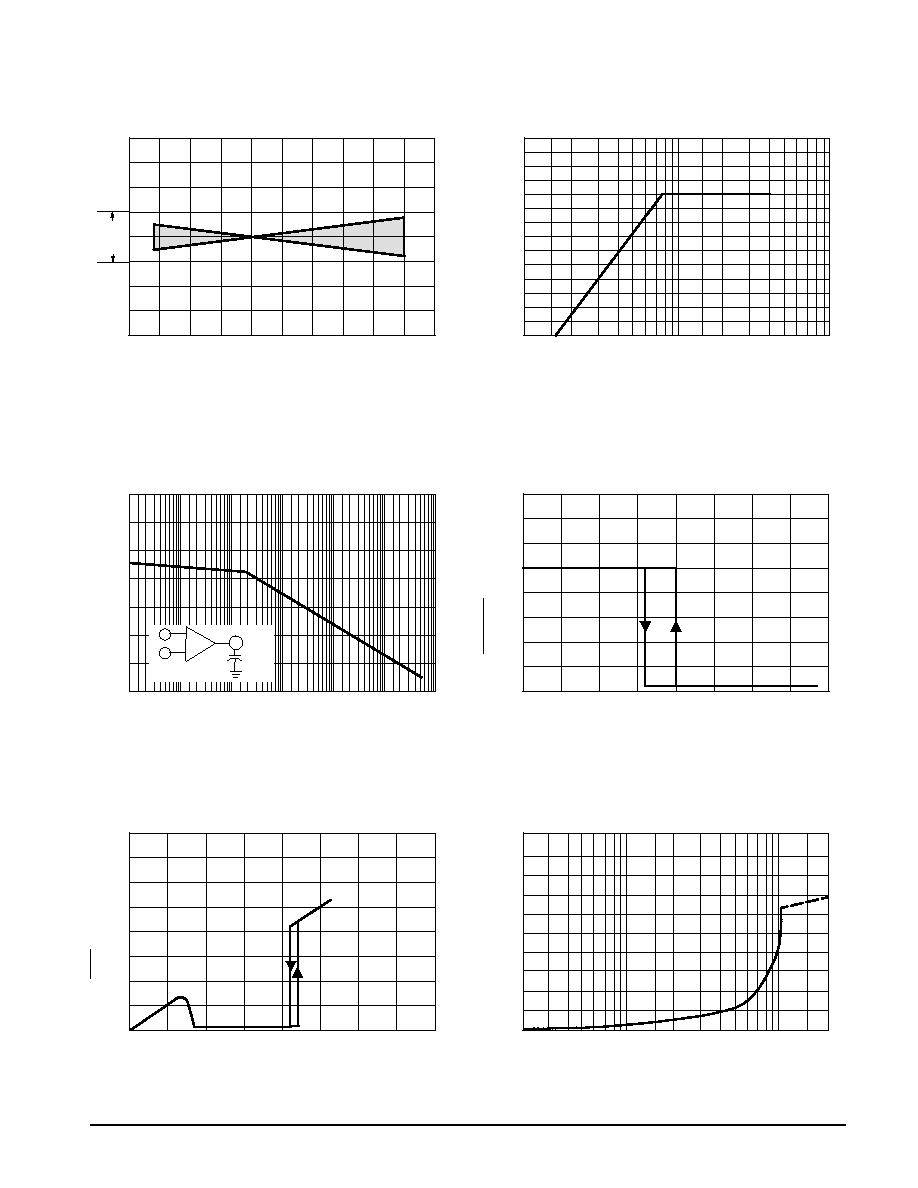
Figure 1. Reference Stability over Temperature
Figure 2. Reference Voltage as a
Function Supply Voltage
Figure 3. Error Amplifier Open Loop
Frequency Response
Figure 4. Current Limit Comparator Threshold
Figure 5. Undervoltage Lockout Characteristic
Figure 6. Output Driver Saturation Voltage as a
Function of Sink Current
≠75
≠50
≠25
0
25
50
75
100
125
150
TJ, JUNCTION TEMPERATURE (
∞
C)
50 mV
Spec
Limit
1.0
2.0
3.0 4.0 5.0
10
20
30 40
VCC, SUPPLY VOLTAGE (V)
, REFERENCE VOL
T
AGE (V)
ref
V
1
2
3
+
_
10
100
1.0 k
10 k
100 k
1.0 M
10 M
100 pF
CComp
f, FREQUENCY (Hz)
,
VOL
T
AGE GAIN (dB)
Vo
l
A
25
50
75
100
125
150
175
200
DIFFERENTIAL INPUT VOLTAGE (mV)
SHUTDOWN VOL
T
AGE (V)
0
1.0
2.0
3.0
4.0
5.0
6.0
7.0
8.0
Vref, REFERENCE VOLTAGE (V)
RESET
VOL
T
AGE
(V)
2.0
5.0
10
20
50
100
200
OUTPUT DRIVER SINK CURRENT (mA)
, OUTPUT
DRIVER SA
TURA
TION VOL
T
AGE (V)
sat
V
5.0
4.0
3.0
2.0
1.0
80
60
40
20
0
8.0
7.0
6.0
5.0
4.0
3.0
2.0
1.0
0
8.0
7.0
6.0
5.0
4.0
3.0
2.0
1.0
0
2.5
2.0
1.5
1.0
0.5
0