5-421
FAST AND LS TTL DATA
DUAL 4-BIT
ADDRESSABLE LATCH
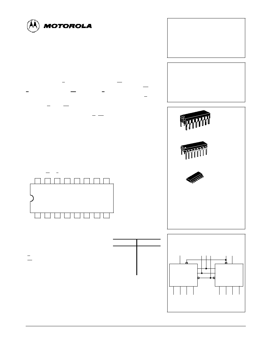
The SN54/74LS256 is a Dual 4-Bit Addressable Latch with common control
inputs; these include two Address inputs (A0, A1), an active LOW Enable input
(E) and an active LOW Clear input (CL). Each latch has a Data input (D) and
four outputs (Q0≠Q3).
When the Enable (E) is HIGH and the Clear input (CL) is LOW, all outputs
(Q0≠Q3) are LOW. Dual 4-channel demultiplexing occurs when the (CL) and
E are both LOW. When CL is HIGH and E is LOW, the selected output
(Q0≠Q3), determined by the Address inputs, follows D. When the E goes
HIGH, the contents of the latch are stored. When operating in the addressable
latch mode (E = LOW, CL = HIGH), changing more than one bit of the Address
(A0, A1) could impose a transient wrong address. Therefore, this should be
done only while in the memory mode (E= CL = HIGH).
∑
Serial-to-Parallel Capability
∑
Output From Each Storage Bit Available
∑
Random (Addressable) Data Entry
∑
Easily Expandable
∑
Active Low Common Clear
∑
Input Clamp Diodes Limit High Speed Termination Effects
14
13
12
11
10
9
1
2
3
4
5
6
7
16
15
8
VCC
A0
CL
E
Db Q3b
Q1b
Q2b
Q0b
A1
Da
Q0a Q1a Q2a Q3a GND
CONNECTION DIAGRAM DIP (TOP VIEW)
NOTE:
The Flatpak version
has the same pinouts
(Connection Diagram) as
the Dual In-Line Package.
PIN NAMES
LOADING (Note a)
HIGH
LOW
A0, A1
Address Inputs
0.5 U.L.
0.25 U.L.
Da, Db
Data Inputs
0.5 U.L.
0.25 U.L.
E
Enable Input (Active LOW)
1.0 U.L.
0.5 U.L.
CL
Clear Input (Active LOW)
0.5 U.L.
0.25 U.L.
Q0a ≠ Q3a,
Q0b ≠ Q3b
Parallel Latch Outputs (Note b)
10 U.L.
5 (2.5) U.L.
NOTES:
a) 1 TTL Unit Load (U.L.) = 40
µ
A HIGH/1.6 mA LOW.
b) The Output LOW drive factor is 2.5 U.L. for Military (54) and 5 U.L. for Commercial
(74) Temperature Ranges.
SN54/74LS256
DUAL 4-BIT
ADDRESSABLE LATCH
LOW POWER SCHOTTKY
ORDERING INFORMATION
SN54LSXXXJ
Ceramic
SN74LSXXXN
Plastic
SN74LSXXXD
SOIC
J SUFFIX
CERAMIC
CASE 620-09
N SUFFIX
PLASTIC
CASE 648-08
16
1
16
1
16
1
D SUFFIX
SOIC
CASE 751B-03
4
5 6
7
9 10 11 12
3
2 1 15
14 13
Da E A0
A1
CL
Q0a Q1a Q2a Q3a
Q0b Q1b Q2b Q3b
LOGIC SYMBOL
VCC = PIN 16
GND = PIN 8
E Db
A0
A1
CL
5-422
FAST AND LS TTL DATA
SN54/74LS256
LOGIC DIAGRAM
E
Da
A0
A1
CL
Db
Q0a
Q1a
Q2a
Q3a
Q0b
Q1b
Q2b
Q3b
14
1
2
6
7
3
4
5
9
11
12
10
13
15
VCC = PIN 16
GND = PIN 8
= PIN NUMBERS
TRUTH TABLE
CL
E
D
A0
A1
Q0
Q1
Q2
Q3
MODE
L
H
X
X
X
L
L
L
L
Clear
L
L
L
L
L
L
L
L
L
Demultiplex
L
L
H
L
L
H
L
L
L
L
L
L
H
L
L
L
L
L
L
L
H
H
L
L
H
L
L
L
L
L
L
H
L
L
L
L
L
L
H
L
H
L
L
H
L
L
L
L
H
H
L
L
L
L
L
L
H
H
H
L
L
L
H
H
H
X
X
X
QN≠1
QN≠1
QN≠1
QN≠1
Memory
H
L
L
L
L
L
QN≠1
QN≠1
QN≠1
Addressable
H
L
H
L
L
H
QN≠1
QN≠1
QN≠1
Latch
H
L
L
H
L
QN≠1
L
QN≠1
QN≠1
H
L
H
H
L
QN≠1
H
QN≠1
QN≠1
H
L
L
L
H
QN≠1
QN≠1
L
QN≠1
H
L
H
L
H
QN≠1
QN≠1
H
QN≠1
H
L
L
H
H
QN≠1
QN≠1
QN≠1
L
H
L
H
H
H
QN≠1
QN≠1
QN≠1
H
H = HIGH Voltage Level
L = LOW Voltage Level
X = Immaterial
MODE SELECTION
E
CL
MODE
L
H
Addressable Latch
H
H
Memory
L
L
Dual 4-Channel Demultiplexer
H
L
Clear
5-423
FAST AND LS TTL DATA
SN54/74LS256
GUARANTEED OPERATING RANGES
Symbol
Parameter
Min
Typ
Max
Unit
VCC
Supply Voltage
54
74
4.5
4.75
5.0
5.0
5.5
5.25
V
TA
Operating Ambient Temperature Range
54
74
≠ 55
0
25
25
125
70
∞
C
IOH
Output Current -- High
54, 74
≠ 0.4
mA
IOL
Output Current -- Low
54
74
4.0
8.0
mA
DC CHARACTERISTICS OVER OPERATING TEMPERATURE RANGE
(unless otherwise specified)
Symbol
Parameter
Limits
Unit
Test Conditions
Symbol
Parameter
Min
Typ
Max
Unit
Test Conditions
VIH
Input HIGH Voltage
2.0
V
Guaranteed Input HIGH Voltage for
All Inputs
VIL
Input LOW Voltage
54
0.7
V
Guaranteed Input LOW Voltage for
All Inputs
VIL
Input LOW Voltage
74
0.8
V
Guaranteed Input LOW Voltage for
All Inputs
VIK
Input Clamp Diode Voltage
≠ 0.65
≠ 1.5
V
VCC = MIN, IIN = ≠ 18 mA
VOH
Output HIGH Voltage
54, 74
2.4
3.5
V
VCC = MIN, IOH = MAX, VIN = VIH
or VIL per Truth Table
VOL
Output LOW Voltage
54, 74
0.25
0.4
V
IOL = 4.0 mA
VCC = VCC MIN,
VIN = VIL or VIH
per Truth Table
VOL
Output LOW Voltage
74
0.35
0.5
V
IOL = 8.0 mA
VIN = VIL or VIH
per Truth Table
IIH
Input HIGH Current
Others
E Input
20
40
µ
A
VCC = MAX, VIN = 2.7 V
IIH
Others
E Input
0.1
0.2
mA
VCC = MAX, VIN = 7.0 V
IIL
Input LOW Current
Others
E Input
≠ 0.4
≠ 0.8
mA
VCC = MAX, VIN = 0.4 V
IOS
Short Circuit Current (Note 1)
≠ 20
≠ 100
mA
VCC = MAX
ICC
Power Supply Current
30
mA
VCC = MAX
Note 1: Not more than one output should be shorted at a time, nor for more than 1 second.
AC CHARACTERISTICS
(TA = 25
∞
C)
Symbol
Parameter
Limits
Unit
Test Conditions
Symbol
Parameter
Min
Typ
Max
Unit
Test Conditions
tPLH
tPHL
Turn-Off Delay, Enable to Output
Turn-On Delay, Enable to Output
20
16
27
24
ns
ns
Figure 1
VCC = 5.0 V,
CL = 15 pF
tPLH
tPHL
Turn-Off Delay, Data to Output
Turn-On Delay, Data to Output
20
13
30
20
ns
ns
Figure 2
VCC = 5.0 V,
CL = 15 pF
tPLH
tPHL
Turn-Off Delay, Address to Output
Turn-On Delay, Address to Output
20
14
30
24
ns
ns
Figure 3
CL = 15 pF
tPHL
Turn-On Delay, Clear to Output
12
23
ns
Figure 5
5-424
FAST AND LS TTL DATA
SN54/74LS256
AC SET-UP REQUIREMENTS
(TA = 25
∞
C)
Symbol
Parameter
Limits
Unit
Test Conditions
Symbol
Parameter
Min
Typ
Max
Unit
Test Conditions
ts
Data Setup Time
20
ns
Figures 4 & 6
VCC = 5.0 V
ts
Address Setup Time
0
ns
Figures 4 & 6
VCC = 5.0 V
th
Data Hold Time
0
ns
Figure 4
VCC = 5.0 V
th
Address Hold Time
15
ns
Figure 6
CC = 5.0 V
tW
Enable Pulse Width
15
ns
Figure 1
ts
Figure 1. Turn-on and Turn-off Delays, Enable To
Output and Enable Pulse Width
Figure 4. Setup and Hold Time, Data to Enable
Figure 2. Turn-on and Turn-off Delays,
Data to Output
Figure 3. Turn-on and Turn-off Delays,
Address to Output
Figure 5. Turn-on Delay, Clear to Output
Figure 6. Setup Time, Address to Enable
(See Notes 1 and 2)
NOTES:
1. The Address to Enable Setup Time is the time before the HIGH-to-LOW Enable transition that the Address must be stable so that the correct latch is
addressed and the other latches are not affected.
2. The shaded areas indicate when the inputs are permitted to change for predictable output performance.
OTHER CONDITIONS: CL = H, A = STABLE
OTHER CONDITIONS: E = L, CL = H, A = STABLE
OTHER CONDITIONS: E = L, CL = L, D = H
OTHER CONDITIONS: C = H, A = STABLE
OTHER CONDITIONS: E = H
1.3 V
tPHL
tPLH
1.3 V
D
E
Q
1.3 V
1.3 V
1.3 V
1.3 V
tPLH
tPHL
D
Q
1.3 V
1.3 V
tPHL
C
Q
1.3 V
1.3 V
1.3 V
1.3 V
1.3 V
1.3 V
A1
A1
Q1
tPLH
D
E
Q
th(H)
th(L)
1.3 V
OTHER CONDITIONS: CL = H
STABLE ADDRESS
A
E
1.3 V
1.3 V
ts(H)
ts(L)
tPHL
th
tpw
tpw
Q=D
Q=D
AC WAVEFORMS
5-425
FAST AND LS TTL DATA
MIN
MIN
MAX
MAX
MILLIMETERS
INCHES
DIM
A
B
C
D
F
G
J
K
M
P
R
9.80
3.80
1.35
0.35
0.40
0.19
0.10
0
∞
5.80
0.25
10.00
4.00
1.75
0.49
1.25
0.25
0.25
7
∞
6.20
0.50
0.386
0.150
0.054
0.014
0.016
0.008
0.004
0
∞
0.229
0.010
0.393
0.157
0.068
0.019
0.049
0.009
0.009
7
∞
0.244
0.019
1.27 BSC
0.050 BSC
NOTES:
1. DIMENSIONING AND TOLERANCING PER ANSI
Y14.5M, 1982.
2. CONTROLLING DIMENSION: MILLIMETER.
3. DIMENSION A AND B DO NOT INCLUDE MOLD
PROTRUSION.
4. MAXIMUM MOLD PROTRUSION 0.15 (0.006)
PER SIDE.
5. 751B 01 IS OBSOLETE, NEW STANDARD
751B 03.
1
8
9
16
-A-
-B-
P
16 PL
D
-T-
K
C
G
M
R X 45
∞
F
J
8 PL
SEATING
PLANE
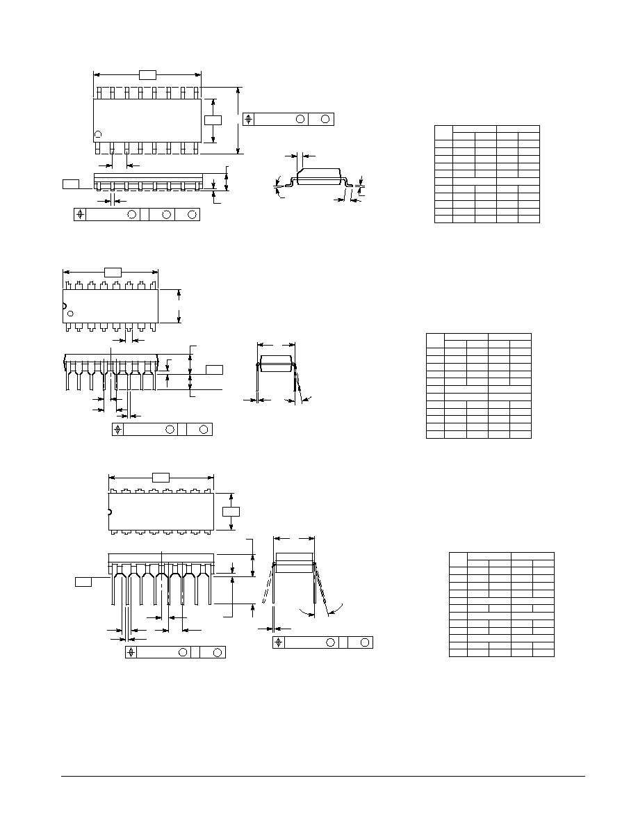
Case 751B-03 D Suffix
16-Pin Plastic
SO-16
B
0.25 (0.010)
M
M
T
0.25 (0.010)
B
A
M
S
S
Case 648-08 N Suffix
16-Pin Plastic
MIN
MIN
MAX
MAX
MILLIMETERS
INCHES
DIM
A
B
C
D
F
G
H
J
K
L
M
S
18.80
6.35
3.69
0.39
1.02
0.21
2.80
7.50
0
∞
0.51
19.55
6.85
4.44
0.53
1.77
0.38
3.30
7.74
10
∞
1.01
0.740
0.250
0.145
0.015
0.040
0.008
0.110
0.295
0
∞
0.020
0.770
0.270
0.175
0.021
0.070
0.015
0.130
0.305
10
∞
0.040
NOTES:
1. DIMENSIONING AND TOLERANCING PER ANSI
Y14.5M, 1982.
2. CONTROLLING DIMENSION: INCH.
3. DIMENSION L" TO CENTER OF LEADS WHEN
FORMED PARALLEL.
4. DIMENSION B" DOES NOT INCLUDE MOLD
FLASH.
5. ROUNDED CORNERS OPTIONAL.
6. 648 01 THRU 07 OBSOLETE, NEW STANDARD
648 08.
2.54 BSC
1.27 BSC
0.100 BSC
0.050 BSC
-A-
B
1
8
9
16
F
H
G
D
16 PL
S
C
-T-
SEATING
PLANE
K
J
M
L
T A
0.25 (0.010)
M
M
Case 620-09 J Suffix
16-Pin Ceramic Dual In-Line
MIN
MIN
MAX
MAX
MILLIMETERS
INCHES
DIM
19.05
6.10
0.39
1.40
0.23
0
∞
0.39
19.55
7.36
4.19
0.53
1.77
0.27
5.08
15
∞
0.88
0.750
0.240
0.015
0.055
0.009
0
∞
0.015
0.770
0.290
0.165
0.021
0.070
0.011
0.200
15
∞
0.035
1.27 BSC
2.54 BSC
7.62 BSC
0.050 BSC
0.100 BSC
0.300 BSC
A
B
C
D
E
F
G
J
K
L
M
N
NOTES:
1. DIMENSIONING AND TOLERANCING PER ANSI
Y14.5M, 1982.
2. CONTROLLING DIMENSION: INCH.
3. DIMENSION L TO CENTER OF LEAD WHEN
FORMED PARALLEL.
4. DIM F MAY NARROW TO 0.76 (0.030) WHERE
THE LEAD ENTERS THE CERAMIC BODY.
5. 620 01 THRU 08 OBSOLETE, NEW STANDARD
620 09.
-B-
-A-
16 PL
-T-
C
D
E
F
G
J
K
M
N
SEATING
PLANE
16 PL
L
16
9
1
8
0.25 (0.010)
T A
M
S
0.25 (0.010)
T B
M
S
5-426
FAST AND LS TTL DATA
Motorola reserves the right to make changes without further notice to any products herein. Motorola makes no warranty, representation or guarantee regarding
the suitability of its products for any particular purpose, nor does Motorola assume any liability arising out of the application or use of any product or circuit,
and specifically disclaims any and all liability, including without limitation consequential or incidental damages. "Typical" parameters can and do vary in different
applications. All operating parameters, including "Typicals" must be validated for each customer application by customer's technical experts. Motorola does
not convey any license under its patent rights nor the rights of others. Motorola products are not designed, intended, or authorized for use as components in
systems intended for surgical implant into the body, or other applications intended to support or sustain life, or for any other application in which the failure of
the Motorola product could create a situation where personal injury or death may occur. Should Buyer purchase or use Motorola products for any such
unintended or unauthorized application, Buyer shall indemnify and hold Motorola and its officers, employees, subsidiaries, affiliates, and distributors harmless
against all claims, costs, damages, and expenses, and reasonable attorney fees arising out of, directly or indirectly, any claim of personal injury or death
associated with such unintended or unauthorized use, even if such claim alleges that Motorola was negligent regarding the design or manufacture of the part.
Motorola and
are registered trademarks of Motorola, Inc. Motorola, Inc. is an Equal Opportunity/Affirmative Action Employer.
Literature Distribution Centers:
USA: Motorola Literature Distribution; P.O. Box 20912; Phoenix, Arizona 85036.
EUROPE: Motorola Ltd.; European Literature Centre; 88 Tanners Drive, Blakelands, Milton Keynes, MK14 5BP, England.
JAPAN: Nippon Motorola Ltd.; 4-32-1, Nishi-Gotanda, Shinagawa-ku, Tokyo 141, Japan.
ASIA PACIFIC: Motorola Semiconductors H.K. Ltd.; Silicon Harbour Center, No. 2 Dai King Street, Tai Po Industrial Estate, Tai Po, N.T., Hong Kong.