5-609
FAST AND LS TTL DATA
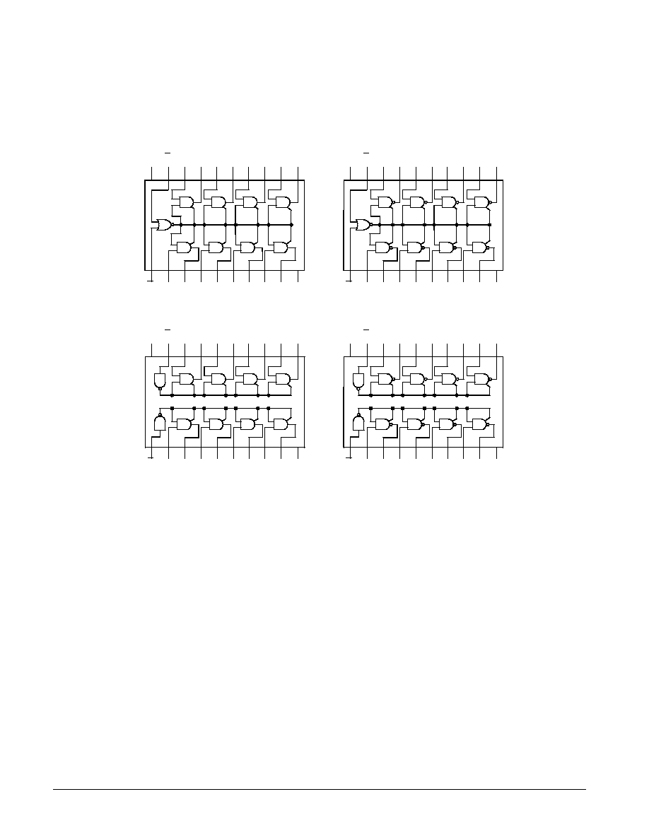
TRI-STATE OCTAL BUFFERS
The SN54 / 74LS795 thru SN54 / 74LS798 device types provide a second
source for the 71 / 81LS95 thru 71 / 81LS98 series. These devices are octal
low power Schottky versions of the 70/8095 thru 70/8098 3-STATE Hex
Buffers. The LS795 and LS797 are noninverting and the LS796 and LS798
are inverting functions. On each buffer, one of the two inputs is used as a
control line to gate the output into the high impedance state, while the other
input passes the data through the buffer. On the LS795 and LS796 access is
through a 2-input NOR gate, with all eight 3-STATE enable lines common. On
the LS797 and LS798, four buffers are enabled from one common line and the
other four buffers from another common line. On all device types the 3-STATE
condition is achieved by applying a high logic level to the enable pins.
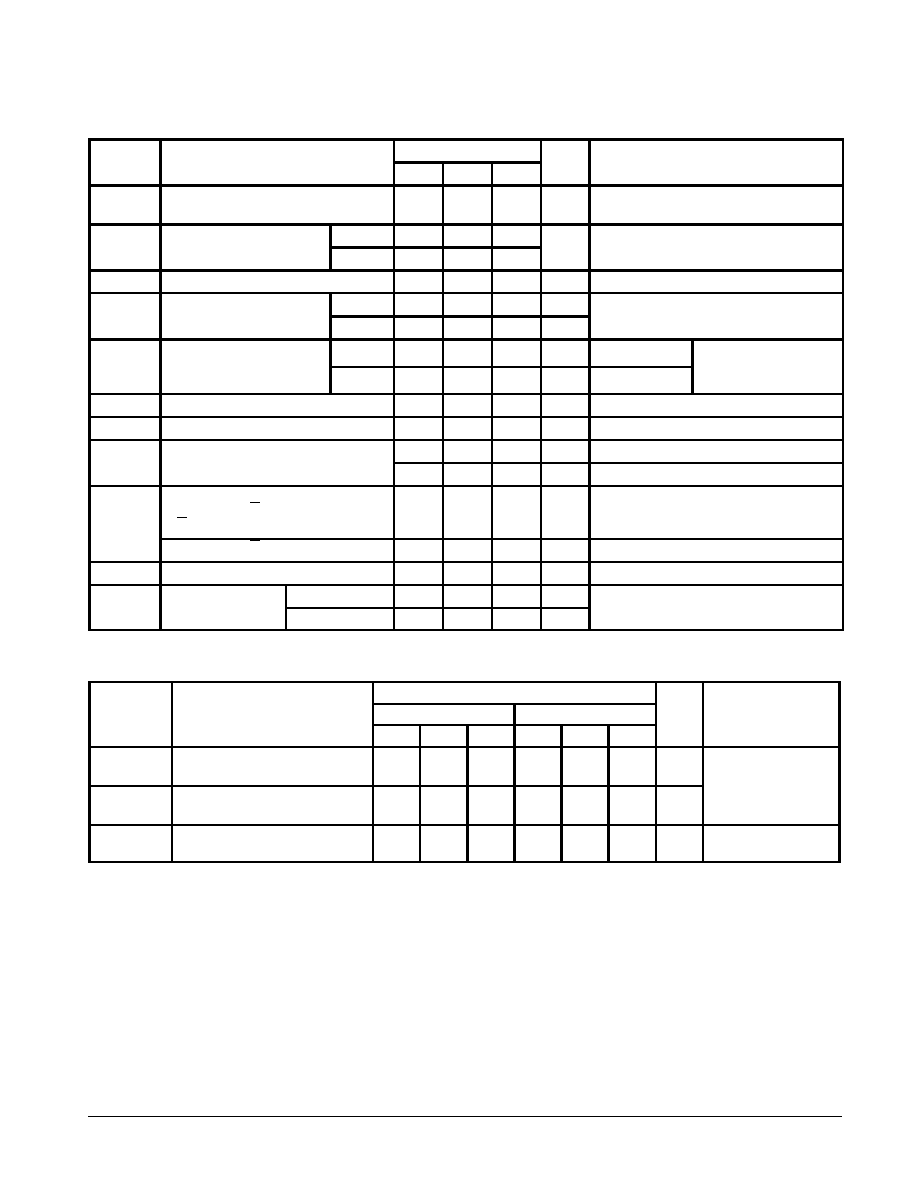
TRUTH TABLES
LS795
INPUTS
OUTPUT
G1
G2
A
Y
H
X
L
L
X
H
L
L
X
X
H
L
Z
Z
H
L
LS796
INPUTS
OUTPUT
G1
G2
A
Y
H
X
L
L
X
H
L
L
X
X
H
L
Z
Z
L
H
LS797
INPUTS
OUTPUT
G
A
Y
H
L
L
X
H
L
Z
H
L
LS798
INPUTS
OUTPUT
G
A
Y
H
L
L
X
H
L
Z
L
H
GUARANTEED OPERATING RANGES
Symbol
Parameter
Min
Typ
Max
Unit
VCC
Supply Voltage
54
74
4.5
4.75
5.0
5.0
5.5
5.25
V
TA
Operating Ambient Temperature Range
54
74
� 55
0
25
25
125
70
�
C
IOH
Output Current -- High
54
74
� 2.6
� 5.0
mA
IOL
Output Current -- Low
54
74
8.0
16
mA
SN54/74LS795
SN54/74LS796
SN54/74LS797
SN54/74LS798
TRI-STATE OCTAL BUFFERS
LOW POWER SCHOTTKY
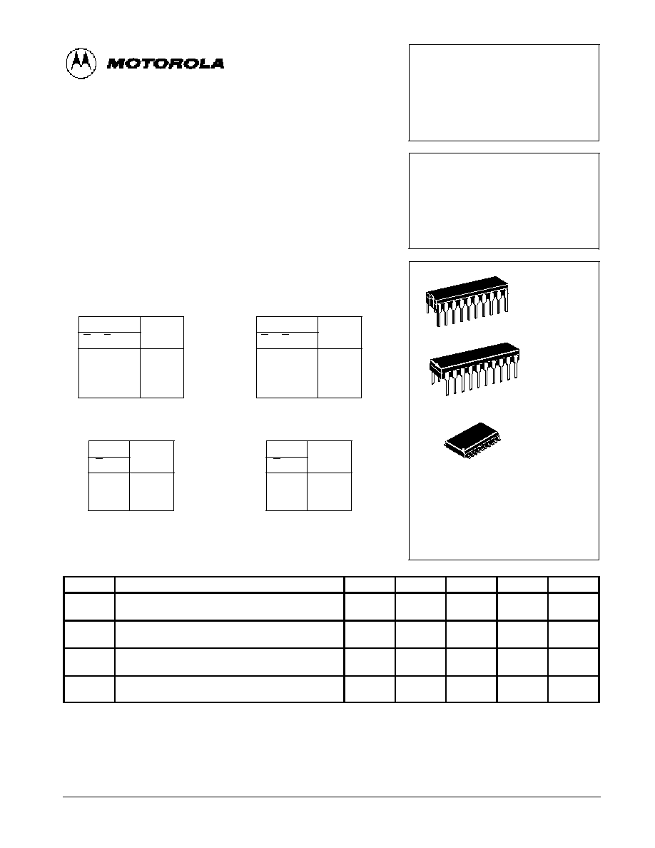
ORDERING INFORMATION
SN54LSXXXJ
Ceramic
SN74LSXXXN
Plastic
SN74LSXXXDW SOIC
20
1
J SUFFIX
CERAMIC
CASE 732-03
20
1
N SUFFIX
PLASTIC
CASE 738-03
20
1
DW SUFFIX
SOIC
CASE 751D-03
5-610
FAST AND LS TTL DATA
SN54/74LS795
�
SN54/74LS796
SN54/74LS797
�
SN54/74LS798
SN54/74LS795
SN54/74LS796
SN54/74LS797
SN54/74LS798
VCC G2
G1
A8 Y8 A7 Y7 A6 Y6 A5 Y5
20 19 18 17 16 15 14 13 12 11
1
2
3
4
5
6
7
8
9
10
A1 Y1 A2 Y2 A3 Y3 A4 Y4 GND
VCC G2
G1
A8 Y8 A7 Y7 A6 Y6 A5 Y5
20 19 18 17 16 15 14 13 12 11
1
2
3
4
5
6
7
8
9
10
A1 Y1 A2 Y2 A3 Y3 A4 Y4 GND
VCC G2
G1
A8 Y8 A7 Y7 A6 Y6 A5 Y5
20 19 18 17 16 15 14 13 12 11
1
2
3
4
5
6
7
8
9
10
A1 Y1 A2 Y2 A3 Y3 A4 Y4 GND
VCC G2
G1
A8 Y8 A7 Y7 A6 Y6 A5 Y5
20 19 18 17 16 15 14 13 12 11
1
2
3
4
5
6
7
8
9
10
A1 Y1 A2 Y2 A3 Y3 A4 Y4 GND
LOGIC DIAGRAMS
5-611
FAST AND LS TTL DATA
SN54/74LS795 THRU SN54/74LS798
DC CHARACTERISTICS OVER OPERATING TEMPERATURE RANGE
(unless otherwise specified)
Symbol
Parameter
Limits
Unit
Test Conditions
Symbol
Parameter
Min
Typ
Max
Unit
Test Conditions
VIH
Input HIGH Voltage
2.0
V
Guaranteed Input HIGH Voltage for
All Inputs
VIL
Input LOW Voltage
54
0.7
V
Guaranteed Input LOW Voltage for
All Inputs
VIL
Input LOW Voltage
74
0.8
V
Guaranteed Input LOW Voltage for
All Inputs
VIK
Input Clamp Diode Voltage
� 0.65
� 1.5
V
VCC = MIN, IIN = � 18 mA
VOH
Output HIGH Voltage
54
2.5
3.5
V
VCC = MIN, IOH = MAX
VOH
Output HIGH Voltage
74
2.7
3.5
V
VCC = MIN, IOH = MAX
VOL
Output LOW Voltage
54, 74
0.25
0.4
V
IOL = 8.0 mA
VCC = VCC MIN,
VIN = VIL or VIH
per Truth Table
VOL
Output LOW Voltage
74
0.35
0.5
V
IOL = 16 mA
VIN = VIL or VIH
per Truth Table
IOZH
Output Off Current -- HIGH
20
�
A
VCC = MAX, VOUT = 2.7 V
IOZL
Output Off Current -- LOW
� 20
�
A
VCC = MAX, VOUT = 0.4 V
IIH
Input HIGH Current
20
�
A
VCC = MAX, VIN = 2.7 V
IIH
Input HIGH Current
� 0.1
mA
VCC = MAX, VIN = 7.0 V
IIL
Input LOW Current
A Input, Both G at 0.4 V
G Input
� 0.4
� 0.4
mA
VCC = MAX, VIN = 0.4 V
A Input, Both G at 2.0 V
� 20
�
A
VCC = MAX, VIN = 0.5 V
IOS
Short Circuit Current (Note 1)
� 30
�130
mA
VCC = MAX
ICC
Power Supply
Current
LS795/LS797
26
mA
VCC = MAX
ICC
Power Supply
Current
LS795/LS798
21
mA
VCC = MAX
Note 1: Not more than one output should be shorted at a time, nor for more than 1 second.
AC CHARACTERISTICS
(TA = 25
�
C)
Symbol
Parameter
Limits
Unit
Test Conditions
Symbol
Parameter
LS795 / LS797
LS796 / LS798
Unit
Test Conditions
Symbol
Parameter
Min
Typ
Max
Min
Typ
Max
Unit
Test Conditions
tPLH
tPHL
Propagation Delay
11
15
16
22
6.0
13
10
17
ns
VCC = 5.0 V
CL = 15 pF
tPZH
tPZL
Output Enable Time
16
13
25
20
17
16
27
25
ns
VCC = 5.0 V
CL = 15 pF
tPHZ
tPLZ
Output Disable Time
13
19
20
27
13
18
20
27
ns
CL = 5.0 pF
5-612
FAST AND LS TTL DATA
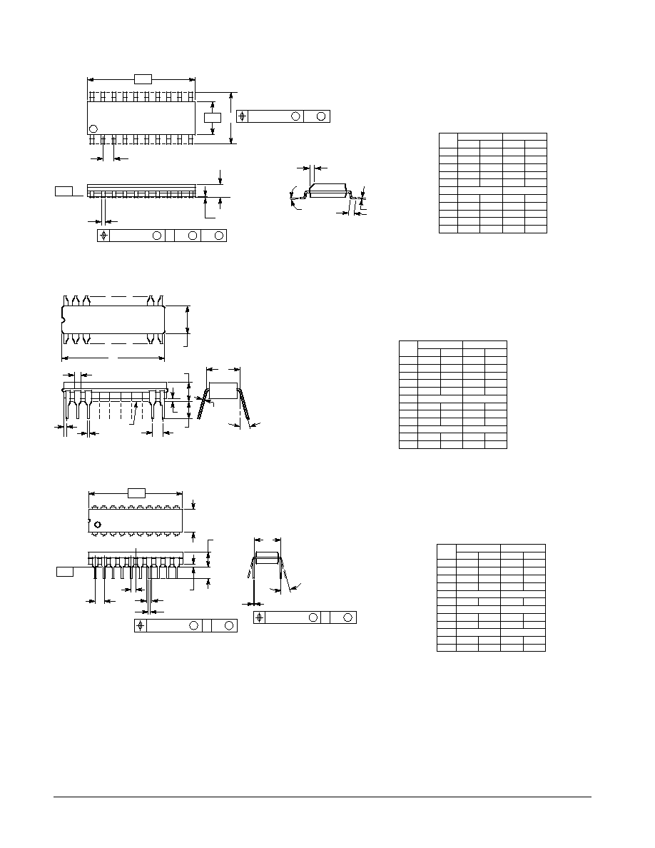
NOTES:
1. DIMENSIONING AND TOLERANCING PER ANSI
Y14.5M, 1982.
2. CONTROLLING DIMENSION: MILLIMETER.
3. DIMENSION A AND B DO NOT INCLUDE MOLD
PROTRUSION.
4. MAXIMUM MOLD PROTRUSION 0.15 (0.006) PER
SIDE.
5. 751D 01, AND 02 OBSOLETE, NEW STANDARD
751D 03.
MIN
MIN
MAX
MAX
MILLIMETERS
INCHES
DIM
A
B
C
D
F
G
J
K
M
P
R
12.65
7.40
2.35
0.35
0.50
0.25
0.10
0
�
10.05
0.25
12.95
7.60
2.65
0.49
0.90
0.32
0.25
7
�
10.55
0.75
0.499
0.292
0.093
0.014
0.020
0.010
0.004
0
�
0.395
0.010
0.510
0.299
0.104
0.019
0.035
0.012
0.009
7
�
0.415
0.029
1.27 BSC
0.050 BSC
-A-
-B-
P
10 PL
1
10
11
20
G
-T-
D
20 PL
K
C
SEATING
PLANE
R X 45
�
M
F
J
Case 751D-03 DW Suffix
20-Pin Plastic
SO-20 (WIDE)
B
0.25 (0.010)
M
M
T
0.25 (0.010)
B
A
M
S
S
Case 732-03 J Suffix
20-Pin Ceramic Dual In-Line
NOTES:
1. LEADS WITHIN 0.25 mm (0.010) DIA., TRUE
POSITION AT SEATING PLANE, AT MAXIMUM
MATERIAL CONDITION.
2. DIM L TO CENTER OF LEADS WHEN FORMED
PARALLEL.
3. DIM A AND B INCLUDES MENISCUS.
MIN
MIN
MAX
MAX
MILLIMETERS
INCHES
DIM
23.88
6.60
3.81
0.38
1.40
0.51
0.20
3.18
25.15
7.49
5.08
0.56
1.65
1.27
0.30
4.06
0
�
0.25
0.940
0.260
0.150
0.015
0.055
0.020
0.008
0.125
0.990
0.295
0.200
0.022
0.065
0.050
0.012
0.160
15
�
1.02
2.54 BSC
7.62 BSC
0.100 BSC
0.300 BSC
A
B
C
D
F
G
H
J
K
L
M
N
0
�
0.010
15
�
0.040
B
C
D
G
H
J
M
N
A
L
20
11
1
10
SEATING
PLANE
K
F
Case 738-03 N Suffix
20-Pin Plastic
MIN
MIN
MAX
MAX
MILLIMETERS
INCHES
DIM
25.66
6.10
3.81
0.39
1.27
0.21
2.80
27.17
6.60
4.57
0.55
1.77
0.38
3.55
0
�
0.51
1.010
0.240
0.150
0.015
0.050
0.008
0.110
1.070
0.260
0.180
0.022
0.070
0.015
0.140
15
�
1.01
1.27 BSC
2.54 BSC
7.62 BSC
0.050 BSC
0.100 BSC
0.300 BSC
A
B
C
D
E
F
G
J
K
L
M
N
0
�
0.020
15
�
0.040
NOTES:
1. DIMENSIONING AND TOLERANCING PER ANSI
Y14.5M, 1982.
2. CONTROLLING DIMENSION: INCH.
3. DIMENSION L" TO CENTER OF LEAD WHEN
FORMED PARALLEL.
4. DIMENSION B" DOES NOT INCLUDE MOLD
FLASH.
5. 738 02 OBSOLETE, NEW STANDARD 738 03.
-A-
B
C
K
N
E
G
F
D
20 PL
J
20 PL
L
M
-T-
SEATING
PLANE
1
10
11
20
T A
0.25 (0.010)
M
M
T B
0.25 (0.010)
M
M
5-613
FAST AND LS TTL DATA
SYMBOL
SW1
SW2
tPZH
Open
Closed
tPZL
Closed
Open
tPLZ
Closed
Closed
tPHZ
Closed
Closed
Motorola reserves the right to make changes without further notice to any products herein. Motorola makes no warranty, representation or guarantee regarding
the suitability of its products for any particular purpose, nor does Motorola assume any liability arising out of the application or use of any product or circuit,
and specifically disclaims any and all liability, including without limitation consequential or incidental damages. "Typical" parameters can and do vary in different
applications. All operating parameters, including "Typicals" must be validated for each customer application by customer's technical experts. Motorola does
not convey any license under its patent rights nor the rights of others. Motorola products are not designed, intended, or authorized for use as components in
systems intended for surgical implant into the body, or other applications intended to support or sustain life, or for any other application in which the failure of
the Motorola product could create a situation where personal injury or death may occur. Should Buyer purchase or use Motorola products for any such
unintended or unauthorized application, Buyer shall indemnify and hold Motorola and its officers, employees, subsidiaries, affiliates, and distributors harmless
against all claims, costs, damages, and expenses, and reasonable attorney fees arising out of, directly or indirectly, any claim of personal injury or death
associated with such unintended or unauthorized use, even if such claim alleges that Motorola was negligent regarding the design or manufacture of the part.
Motorola and
are registered trademarks of Motorola, Inc. Motorola, Inc. is an Equal Opportunity/Affirmative Action Employer.
Literature Distribution Centers:
USA: Motorola Literature Distribution; P.O. Box 20912; Phoenix, Arizona 85036.
EUROPE: Motorola Ltd.; European Literature Centre; 88 Tanners Drive, Blakelands, Milton Keynes, MK14 5BP, England.
JAPAN: Nippon Motorola Ltd.; 4-32-1, Nishi-Gotanda, Shinagawa-ku, Tokyo 141, Japan.
ASIA PACIFIC: Motorola Semiconductors H.K. Ltd.; Silicon Harbour Center, No. 2 Dai King Street, Tai Po Industrial Estate, Tai Po, N.T., Hong Kong.