 | –≠–ª–µ–∫—Ç—Ä–æ–Ω–Ω—ã–π –∫–æ–º–ø–æ–Ω–µ–Ω—Ç: TIP36C | –°–∫–∞—á–∞—Ç—å:  PDF PDF  ZIP ZIP |
1
Motorola Bipolar Power Transistor Device Data
Complementary Silicon
High-Power Transistors
. . . for general≠purpose power amplifier and switching applications.
∑
25 A Collector Current
∑
Low Leakage Current -- ICEO = 1.0 mA @ 30 and 60 V
∑
Excellent DC Gain -- hFE = 40 Typ @ 15 A
∑
High Current Gain Bandwidth Product --
hfe
= 3.0 min @ IC = 1.0 A,
f = 1.0 MHz
ŒŒŒŒŒŒŒŒŒŒŒŒŒŒŒŒŒŒŒŒŒŒŒ
ŒŒŒŒŒŒŒŒŒŒŒŒŒŒŒŒŒŒŒŒŒŒŒ
MAXIMUM RATINGS
ŒŒŒŒŒŒŒŒŒŒŒ
Œ
ŒŒŒŒŒŒŒŒŒ
Œ
ŒŒŒŒŒŒŒŒŒŒŒ
Rating
ŒŒŒ
Œ
ŒŒ
ŒŒŒ
Symbol
ŒŒŒŒ
Œ
ŒŒ
Œ
ŒŒŒŒ
TIP35A
TIP36A
ŒŒŒ
Œ
Œ
Œ
ŒŒŒ
TIP35B
TIP36B
ŒŒŒŒ
Œ
ŒŒ
Œ
ŒŒŒŒ
TIP35C
TIP36C
ŒŒŒ
Œ
Œ
Œ
ŒŒŒ
Unit
ŒŒŒŒŒŒŒŒŒŒŒ
ŒŒŒŒŒŒŒŒŒŒŒ
Collector≠Emitter Voltage
ŒŒŒ
ŒŒŒ
VCEO
ŒŒŒŒ
ŒŒŒŒ
60 V
ŒŒŒ
ŒŒŒ
80 V
ŒŒŒŒ
ŒŒŒŒ
100 V
ŒŒŒ
ŒŒŒ
Vdc
ŒŒŒŒŒŒŒŒŒŒŒ
ŒŒŒŒŒŒŒŒŒŒŒ
Collector≠Base Voltage
ŒŒŒ
ŒŒŒ
VCB
ŒŒŒŒ
ŒŒŒŒ
60 V
ŒŒŒ
ŒŒŒ
80 V
ŒŒŒŒ
ŒŒŒŒ
100 V
ŒŒŒ
ŒŒŒ
Vdc
ŒŒŒŒŒŒŒŒŒŒŒ
ŒŒŒŒŒŒŒŒŒŒŒ
Emitter≠Base Voltage
ŒŒŒ
ŒŒŒ
VEB
ŒŒŒŒŒŒŒŒŒ
ŒŒŒŒŒŒŒŒŒ
5.0
ŒŒŒ
ŒŒŒ
Vdc
ŒŒŒŒŒŒŒŒŒŒŒ
Œ
ŒŒŒŒŒŒŒŒŒ
Œ
ŒŒŒŒŒŒŒŒŒŒŒ
Collector Current -- Continuous
Peak (1)
ŒŒŒ
Œ
ŒŒ
ŒŒŒ
IC
ŒŒŒŒŒŒŒŒŒ
Œ
ŒŒŒŒŒŒŒ
Œ
ŒŒŒŒŒŒŒŒŒ
25
40
ŒŒŒ
Œ
Œ
Œ
ŒŒŒ
Adc
ŒŒŒŒŒŒŒŒŒŒŒ
ŒŒŒŒŒŒŒŒŒŒŒ
Base Current -- Continuous
ŒŒŒ
ŒŒŒ
IB
ŒŒŒŒŒŒŒŒŒ
ŒŒŒŒŒŒŒŒŒ
5.0
ŒŒŒ
ŒŒŒ
Adc
ŒŒŒŒŒŒŒŒŒŒŒ
Œ
ŒŒŒŒŒŒŒŒŒ
Œ
ŒŒŒŒŒŒŒŒŒŒŒ
Total Power Dissipation
@ TC = 25
_
C
Derate above 25
_
C
ŒŒŒ
Œ
ŒŒ
ŒŒŒ
PD
ŒŒŒŒŒŒŒŒŒ
Œ
ŒŒŒŒŒŒŒ
Œ
ŒŒŒŒŒŒŒŒŒ
125
1.0
ŒŒŒ
Œ
Œ
Œ
ŒŒŒ
Watts
W/
_
C
ŒŒŒŒŒŒŒŒŒŒŒ
Œ
ŒŒŒŒŒŒŒŒŒ
Œ
ŒŒŒŒŒŒŒŒŒŒŒ
Operating and Storage Junction
Temperature Range
ŒŒŒ
Œ
ŒŒ
ŒŒŒ
TJ, Tstg
ŒŒŒŒŒŒŒŒŒ
Œ
ŒŒŒŒŒŒŒ
Œ
ŒŒŒŒŒŒŒŒŒ
≠ 65 to + 150
ŒŒŒ
Œ
Œ
Œ
ŒŒŒ
_
C
ŒŒŒŒŒŒŒŒŒŒŒ
ŒŒŒŒŒŒŒŒŒŒŒ
Unclamped Inductive Load
ŒŒŒ
ŒŒŒ
ESB
ŒŒŒŒŒŒŒŒŒ
ŒŒŒŒŒŒŒŒŒ
90
ŒŒŒ
ŒŒŒ
mJ
ŒŒŒŒŒŒŒŒŒŒŒŒŒŒŒŒŒŒŒŒŒŒŒ
ŒŒŒŒŒŒŒŒŒŒŒŒŒŒŒŒŒŒŒŒŒŒŒ
THERMAL CHARACTERISTICS
ŒŒŒŒŒŒŒŒŒŒŒŒ
ŒŒŒŒŒŒŒŒŒŒŒŒ
Characteristic
ŒŒŒŒŒ
ŒŒŒŒŒ
Symbol
ŒŒŒŒŒŒ
ŒŒŒŒŒŒ
Max
ŒŒŒ
ŒŒŒ
Unit
ŒŒŒŒŒŒŒŒŒŒŒŒ
ŒŒŒŒŒŒŒŒŒŒŒŒ
Thermal Resistance, Junction to Case
ŒŒŒŒŒ
ŒŒŒŒŒ
R
JC
ŒŒŒŒŒŒ
ŒŒŒŒŒŒ
1.0
ŒŒŒ
ŒŒŒ
_
C/W
ŒŒŒŒŒŒŒŒŒŒŒŒ
ŒŒŒŒŒŒŒŒŒŒŒŒ
Junction≠To≠Free≠Air Thermal Resistance
ŒŒŒŒŒ
ŒŒŒŒŒ
R
JA
ŒŒŒŒŒŒ
ŒŒŒŒŒŒ
35.7
ŒŒŒ
ŒŒŒ
_
C/W
(1) Pulse Test: Pulse Width = 10 ms, Duty Cycle
v
10%.
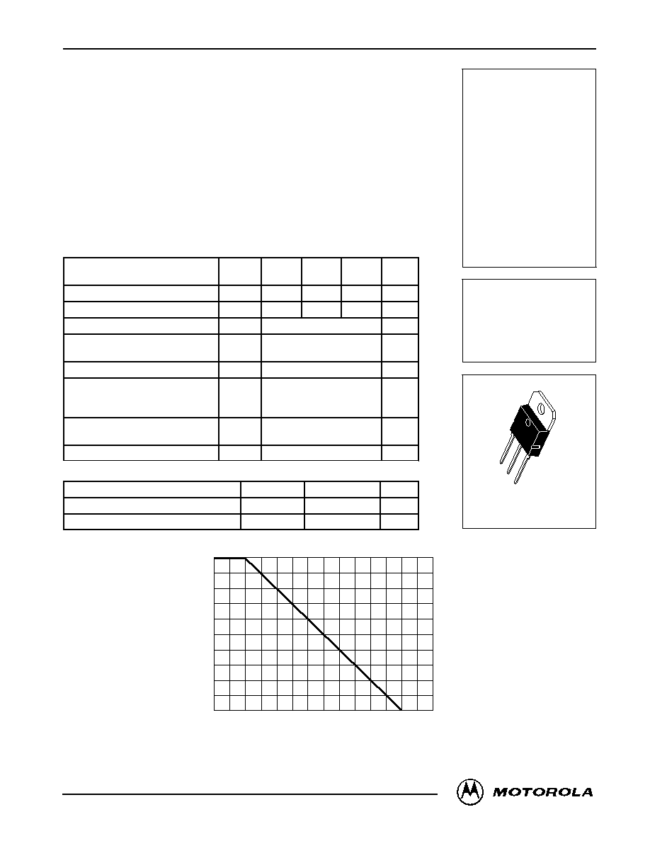
Figure 1. Power Derating
TC, CASE TEMPERATURE (
∞
C)
0
125
0
25
175
75
100
75
100
50
125
25
150
P
D
, POWER DISSIP
A
TION (W
A
TTS)
50
Preferred devices are Motorola recommended choices for future use and best overall value.
MOTOROLA
SEMICONDUCTOR TECHNICAL DATA
Order this document
by TIP35A/D
©
Motorola, Inc. 1996
TIP35A
TIP35B
TIP35C
TIP36A
TIP36B
TIP36C
25 AMPERE
COMPLEMENTARY
SILICON
POWER TRANSISTORS
60 ≠ 100 VOLTS
125 WATTS
*Motorola Preferred Device
*
NPN
PNP
*
*
*
CASE 340D≠02
TO≠218AC
REV 1

TIP35A TIP35B TIP35C TIP36A TIP36B TIP36C
2
Motorola Bipolar Power Transistor Device Data
ŒŒŒŒŒŒŒŒŒŒŒŒŒŒŒŒŒŒŒŒŒŒŒŒŒŒŒŒŒŒŒŒŒŒ
ŒŒŒŒŒŒŒŒŒŒŒŒŒŒŒŒŒŒŒŒŒŒŒŒŒŒŒŒŒŒŒŒŒŒ
ELECTRICAL CHARACTERISTICS
(TC = 25
_
C unless otherwise noted)
ŒŒŒŒŒŒŒŒŒŒŒŒŒŒŒŒŒŒŒŒŒŒŒ
ŒŒŒŒŒŒŒŒŒŒŒŒŒŒŒŒŒŒŒŒŒŒŒ
Characteristic
ŒŒŒŒ
ŒŒŒŒ
Symbol
ŒŒŒŒ
ŒŒŒŒ
Min
ŒŒŒŒ
ŒŒŒŒ
Max
ŒŒŒ
ŒŒŒ
Unit
ŒŒŒŒŒŒŒŒŒŒŒŒŒŒŒŒŒŒŒŒŒŒŒŒŒŒŒŒŒŒŒŒŒŒ
ŒŒŒŒŒŒŒŒŒŒŒŒŒŒŒŒŒŒŒŒŒŒŒŒŒŒŒŒŒŒŒŒŒŒ
OFF CHARACTERISTICS
ŒŒŒŒŒŒŒŒŒŒŒŒŒŒŒŒŒŒŒŒŒŒŒ
Œ
ŒŒŒŒŒŒŒŒŒŒŒŒŒŒŒŒŒŒŒŒŒ
Œ
Œ
ŒŒŒŒŒŒŒŒŒŒŒŒŒŒŒŒŒŒŒŒŒ
Œ
ŒŒŒŒŒŒŒŒŒŒŒŒŒŒŒŒŒŒŒŒŒŒŒ
Collector≠Emitter Sustaining Voltage (1)
(IC = 30 mA, IB = 0)
TIP35A, TIP36A
TIP35B, TIP36B
TIP35C, TIP36C
ŒŒŒŒ
ŒŒŒ
Œ
ŒŒŒ
Œ
ŒŒŒŒ
VCEO(sus)
ŒŒŒŒ
Œ
ŒŒ
Œ
Œ
ŒŒ
Œ
ŒŒŒŒ
60
80
100
ŒŒŒŒ
Œ
ŒŒ
Œ
Œ
ŒŒ
Œ
ŒŒŒŒ
--
--
--
ŒŒŒ
ŒŒ
Œ
ŒŒ
Œ
ŒŒŒ
Vdc
ŒŒŒŒŒŒŒŒŒŒŒŒŒŒŒŒŒŒŒŒŒŒŒ
Œ
ŒŒŒŒŒŒŒŒŒŒŒŒŒŒŒŒŒŒŒŒŒ
Œ
Œ
ŒŒŒŒŒŒŒŒŒŒŒŒŒŒŒŒŒŒŒŒŒ
Œ
ŒŒŒŒŒŒŒŒŒŒŒŒŒŒŒŒŒŒŒŒŒŒŒ
Collector≠Emitter Cutoff Current
(VCE = 30 V, IB = 0)
TIP35A, TIP36A
(VCE = 60 V, IB = 0)
TIP35B, TIP35C, TIP36B, TIP36C
ŒŒŒŒ
ŒŒŒ
Œ
ŒŒŒ
Œ
ŒŒŒŒ
ICEO
ŒŒŒŒ
Œ
ŒŒ
Œ
Œ
ŒŒ
Œ
ŒŒŒŒ
--
--
ŒŒŒŒ
Œ
ŒŒ
Œ
Œ
ŒŒ
Œ
ŒŒŒŒ
1.0
1.0
ŒŒŒ
ŒŒ
Œ
ŒŒ
Œ
ŒŒŒ
mA
ŒŒŒŒŒŒŒŒŒŒŒŒŒŒŒŒŒŒŒŒŒŒŒ
ŒŒŒŒŒŒŒŒŒŒŒŒŒŒŒŒŒŒŒŒŒŒŒ
Collector≠Emitter Cutoff Current
(VCE = Rated VCEO, VEB = 0)
ŒŒŒŒ
ŒŒŒŒ
ICES
ŒŒŒŒ
ŒŒŒŒ
--
ŒŒŒŒ
ŒŒŒŒ
0.7
ŒŒŒ
ŒŒŒ
mA
ŒŒŒŒŒŒŒŒŒŒŒŒŒŒŒŒŒŒŒŒŒŒŒ
Œ
ŒŒŒŒŒŒŒŒŒŒŒŒŒŒŒŒŒŒŒŒŒ
Œ
ŒŒŒŒŒŒŒŒŒŒŒŒŒŒŒŒŒŒŒŒŒŒŒ
Emitter≠Base Cutoff Current
(VEB = 5.0 V, IC = 0)
ŒŒŒŒ
ŒŒŒ
Œ
ŒŒŒŒ
IEBO
ŒŒŒŒ
Œ
ŒŒ
Œ
ŒŒŒŒ
--
ŒŒŒŒ
Œ
ŒŒ
Œ
ŒŒŒŒ
1.0
ŒŒŒ
ŒŒ
Œ
ŒŒŒ
mA
ŒŒŒŒŒŒŒŒŒŒŒŒŒŒŒŒŒŒŒŒŒŒŒŒŒŒŒŒŒŒŒŒŒŒ
ŒŒŒŒŒŒŒŒŒŒŒŒŒŒŒŒŒŒŒŒŒŒŒŒŒŒŒŒŒŒŒŒŒŒ
ON CHARACTERISTICS (1)
ŒŒŒŒŒŒŒŒŒŒŒŒŒŒŒŒŒŒŒŒŒŒŒ
Œ
ŒŒŒŒŒŒŒŒŒŒŒŒŒŒŒŒŒŒŒŒŒ
Œ
ŒŒŒŒŒŒŒŒŒŒŒŒŒŒŒŒŒŒŒŒŒŒŒ
DC Current Gain
(IC = 1.5 A, VCE = 4.0 V)
(IC = 15 A, VCE = 4.0 V)
ŒŒŒŒ
ŒŒŒ
Œ
ŒŒŒŒ
hFE
ŒŒŒŒ
Œ
ŒŒ
Œ
ŒŒŒŒ
25
15
ŒŒŒŒ
Œ
ŒŒ
Œ
ŒŒŒŒ
--
75
ŒŒŒ
ŒŒ
Œ
ŒŒŒ
--
ŒŒŒŒŒŒŒŒŒŒŒŒŒŒŒŒŒŒŒŒŒŒŒ
Œ
ŒŒŒŒŒŒŒŒŒŒŒŒŒŒŒŒŒŒŒŒŒ
Œ
Œ
ŒŒŒŒŒŒŒŒŒŒŒŒŒŒŒŒŒŒŒŒŒ
Œ
ŒŒŒŒŒŒŒŒŒŒŒŒŒŒŒŒŒŒŒŒŒŒŒ
Collector≠Emitter Saturation Voltage
(IC = 15 A, IB = 1.5 A)
(IC = 25 A, IB = 5.0 A)
ŒŒŒŒ
ŒŒŒ
Œ
ŒŒŒ
Œ
ŒŒŒŒ
VCE(sat)
ŒŒŒŒ
Œ
ŒŒ
Œ
Œ
ŒŒ
Œ
ŒŒŒŒ
--
--
ŒŒŒŒ
Œ
ŒŒ
Œ
Œ
ŒŒ
Œ
ŒŒŒŒ
1.8
4.0
ŒŒŒ
ŒŒ
Œ
ŒŒ
Œ
ŒŒŒ
Vdc
ŒŒŒŒŒŒŒŒŒŒŒŒŒŒŒŒŒŒŒŒŒŒŒ
Œ
ŒŒŒŒŒŒŒŒŒŒŒŒŒŒŒŒŒŒŒŒŒ
Œ
ŒŒŒŒŒŒŒŒŒŒŒŒŒŒŒŒŒŒŒŒŒŒŒ
Base≠Emitter On Voltage
(IC = 15 A, VCE = 4.0 V)
(IC = 25 A, VCE = 4.0 V)
ŒŒŒŒ
ŒŒŒ
Œ
ŒŒŒŒ
VBE(on)
ŒŒŒŒ
Œ
ŒŒ
Œ
ŒŒŒŒ
--
--
ŒŒŒŒ
Œ
ŒŒ
Œ
ŒŒŒŒ
2.0
4.0
ŒŒŒ
ŒŒ
Œ
ŒŒŒ
Vdc
ŒŒŒŒŒŒŒŒŒŒŒŒŒŒŒŒŒŒŒŒŒŒŒŒŒŒŒŒŒŒŒŒŒŒ
ŒŒŒŒŒŒŒŒŒŒŒŒŒŒŒŒŒŒŒŒŒŒŒŒŒŒŒŒŒŒŒŒŒŒ
DYNAMIC CHARACTERISTICS
ŒŒŒŒŒŒŒŒŒŒŒŒŒŒŒŒŒŒŒŒŒŒŒ
Œ
ŒŒŒŒŒŒŒŒŒŒŒŒŒŒŒŒŒŒŒŒŒ
Œ
ŒŒŒŒŒŒŒŒŒŒŒŒŒŒŒŒŒŒŒŒŒŒŒ
Small≠Signal Current Gain
(IC = 1.0 A, VCE = 10 V, f = 1.0 kHz)
ŒŒŒŒ
ŒŒŒ
Œ
ŒŒŒŒ
hfe
ŒŒŒŒ
Œ
ŒŒ
Œ
ŒŒŒŒ
25
ŒŒŒŒ
Œ
ŒŒ
Œ
ŒŒŒŒ
--
ŒŒŒ
ŒŒ
Œ
ŒŒŒ
--
ŒŒŒŒŒŒŒŒŒŒŒŒŒŒŒŒŒŒŒŒŒŒŒ
Œ
ŒŒŒŒŒŒŒŒŒŒŒŒŒŒŒŒŒŒŒŒŒ
Œ
ŒŒŒŒŒŒŒŒŒŒŒŒŒŒŒŒŒŒŒŒŒŒŒ
Current≠Gain -- Bandwidth Product
(IC = 1.0 A, VCE = 10 V, f = 1.0 MHz)
ŒŒŒŒ
ŒŒŒ
Œ
ŒŒŒŒ
fT
ŒŒŒŒ
Œ
ŒŒ
Œ
ŒŒŒŒ
3.0
ŒŒŒŒ
Œ
ŒŒ
Œ
ŒŒŒŒ
--
ŒŒŒ
ŒŒ
Œ
ŒŒŒ
MHz
(1) Pulse Test: Pulse Width = 300
µ
s, Duty Cycle
v
2.0%.
Figure 2. Switching Time Equivalent Test Circuits
0.3
Figure 3. Turn≠On Time
IC, COLLECTOR CURRENT (AMPERES)
0.02
1.0
30
0.07
1.0
10
TJ = 25
∞
C
IC/IB = 10
VCC = 30 V
VBE(off) = 2 V
t, TIME
(
s
)
µ
0.5
0.3
0.1
0.05
0.5
3.0
5.0
0.03
0.7
2.0
0.7
7.0
tr
0.2
2.0
20
td
(PNP)
(NPN)
TURN≠ON TIME
TURN≠OFF TIME
+ 2.0 V
0
tr
20 ns
≠11.0 V
10 TO 100
µ
S
3.0
RL
≠ 30 V
VCC
DUTY CYCLE
2.0%
10
RB
TO SCOPE
tr
20 ns
VBB
+ 4.0 V
FOR CURVES OF FIGURES 3 & 4, RB & RL ARE VARIED.
INPUT LEVELS ARE APPROXIMATELY AS SHOWN.
FOR NPN, REVERSE ALL POLARITIES.
0
+ 9.0 V
≠11.0 V
10 to 100
µ
s
tr
20 ns
DUTY CYCLE
2.0%
3.0
RL
≠ 30 V
VCC
10
RB
TO SCOPE
tr
20 ns

TIP35A TIP35B TIP35C TIP36A TIP36B TIP36C
3
Motorola Bipolar Power Transistor Device Data
0.5
1.0
2.0
7.0
0.3
3.0
5.0
0.7
IC, COLLECTOR CURRENT (AMPERES)
Figure 4. Turn≠Off Time
10
t, TIME
(
s
)
µ
7.0
5.0
3.0
2.0
1.0
0.7
0.5
0.3
0.2
0.1
10
20
30
TJ = 25
∞
C
VCC = 30 V
IC/IB = 10
IB1 = IB2
ts
tf
(PNP)
(NPN)
ts
tf
IC, COLLECTOR CURRENT (AMPS)
h
FE
, DC CURRENT
GAIN
Figure 5. DC Current Gain
200
500
0.2
0.5
2.0
100
0.1
100
50
20
10
1.0
VCE = 4.0 V
TJ = 25
∞
C
5.0
10
20
5.0
50
PNP
NPN
1000
2.0
1.0
FORWARD BIAS
There are two limitations on the power handling ability of a
transistor: average junction temperature and second break-
down. Safe operating area curves indicate IC ≠ VCE limits of
the transistor that must be observed for reliable operation;
i.e., the transistor must not be subjected to greater dissipa-
tion than the curves indicate.
The data of Figure 6 is based on TC = 25
_
C; TJ(pk) is
variable depending on power level. Second breakdown pulse
limits are valid for duty cycles to 10% but must be derated
when TC
w
25
_
C. Second breakdown limitations do not der-
ate the same as thermal limitations.
REVERSE BIAS
For inductive loads, high voltage and high current must be
sustained simultaneously during turn≠off, in most cases, with
the base to emitter junction reverse biased. Under these
conditions the collector voltage must be held to a safe level
at or below a specific value of collector current. This can be
accomplished by several means such as active clamping,
RC snubbing, load line shaping, etc. The safe level for these
devices is specified as Reverse Bias Safe Operating Area
and represents the voltage≠current conditions during re-
verse biased turn≠off. This rating is verified under clamped
conditions so that the device is never subjected to an ava-
lanche mode. Figure 7 gives RBSOA characteristics.
VCE, COLLECTOR≠EMITTER VOLTAGE (VOLTS)
7.0
20
1.0
50
100
0.2
0
0.5
SECONDARY BREAKDOWN
THERMAL LIMIT
BONDING WIRE LIMIT
1.0 ms
dc
300
µ
s
2.0
1.0
100
30
I C
, COLLECT
OR
CURRENT
(AMPS)
10 ms
Figure 6. Maximum Rated Forward Bias
Safe Operating Area
50
20
10
5.0
0.3
2.0
3.0
5.0
10
30
70
TC = 25
∞
C
TIP35A, 36A
TIP35B, 36B
TIP35C, 36C
VCE, COLLECTOR≠EMITTER VOLTAGE (VOLTS)
40
60
0
80
100
5.0
0
15
20
40
30
I C
, COLLECT
OR
CURRENT
(AMPS)
Figure 7. Maximum Rated Forward Bias
Safe Operating Area
25
10
10
20
30
50
70
90
TJ
100
∞
C
TIP35A
TIP36A
TIP35B
TIP36B
TIP35C
TIP36C

TIP35A TIP35B TIP35C TIP36A TIP36B TIP36C
4
Motorola Bipolar Power Transistor Device Data
Figure 8. Inductive Load Switching
TEST CIRCUIT
VOLTAGE AND CURRENT WAVEFORMS
NOTES:
A. L1 and L2 are 10 mH, 0.11
, Chicago Standard Transformer Corporation C≠2688, or equivalent.
B. Input pulse width is increased until ICM = ≠ 3.0 A.
C. For NPN, reverse all polarities.
INPUT
50
MJE180
RBB1
20
RBB2 = 100
VBB2 = 0
VBB1 = 10 V
VCE MONITOR
L1
(SEE NOTE A)
L2
(SEE NOTE A)
TUT
VCC = 10 V
IC MONITOR
+
≠
RS = 0.1
50
+
≠
5.0 V
0
≠ 3.0 A
≠10 V
tw = 6.0 ms
(SEE NOTE B)
INPUT
VOLTAGE
COLLECTOR
CURRENT
COLLECTOR
VOLTAGE
V(BR)CER
0
0
100 ms
TIP35A TIP35B TIP35C TIP36A TIP36B TIP36C
5
Motorola Bipolar Power Transistor Device Data
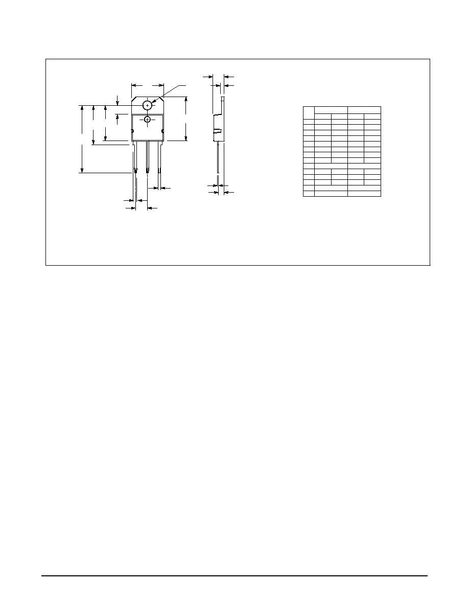
PACKAGE DIMENSIONS
CASE 340D≠02
ISSUE B
NOTES:
1. DIMENSIONING AND TOLERANCING PER ANSI
Y14.5M, 1982.
2. CONTROLLING DIMENSION: MILLIMETER.
A
D
V
G
K
S
L
U
B
Q
E
C
J
H
DIM
MIN
MAX
MIN
MAX
INCHES
MILLIMETERS
A
≠≠≠
20.35
≠≠≠
0.801
B
14.70
15.20
0.579
0.598
C
4.70
4.90
0.185
0.193
D
1.10
1.30
0.043
0.051
E
1.17
1.37
0.046
0.054
G
5.40
5.55
0.213
0.219
H
2.00
3.00
0.079
0.118
J
0.50
0.78
0.020
0.031
K
31.00 REF
1.220 REF
L
≠≠≠
16.20
≠≠≠
0.638
Q
4.00
4.10
0.158
0.161
S
17.80
18.20
0.701
0.717
U
4.00 REF
0.157 REF
V
1.75 REF
0.069
1
2
3
4
STYLE 1:
PIN 1. BASE
2. COLLECTOR
3. EMITTER
4. COLLECTOR