
MOTOROLA
SEMICONDUCTOR TECHNICAL DATA
DSP56011
Order this document by:
DSP56011/D
� MOTOROLA, INC. 1996, 1997
Preliminary Information
This document contains information on a new product. Specifications and information herein are subject to change without notice.
PRELIMINARY
Advance Information
24-BIT DVD DIGITAL SIGNAL PROCESSOR
The DSP56011 is a high-performance programmable Digital Signal Processor (DSP) developed
for Digital Versatile Disc (DVD), High-Definition Television (HDTV), and Advanced Set-top
audio decoding. The DSP56011 is optimized with audio-specific peripherals and customized
memory configuration, and may be programmed with Motorola's certified software for Dolby
AC-3
5.1 Channel Surround, Dolby Pro Logic, and MPEG1 Layer 2. These applications use
Motorola's 24-bit DSP56000 architecture and are the highest quality solutions available. Flexible
peripheral modules and interface software allow simple connection to a wide variety of video/
system decoders. In addition, the DSP56011 offers switchable memory space configuration, a
large user-definable Program ROM and two independent data RAMs and ROMs, a Serial Audio
Interface (SAI), Serial Host Interface (SHI), Parallel Host Interface (HI) with Direct Memory
Access (DMA) for communicating with other processors, dedicated I/O lines, on-chip Phase
Lock Loop (PLL), On-Chip Emulation (OnCE
TM
) port, and on-chip Digital Audio Transmitter
(DAX).
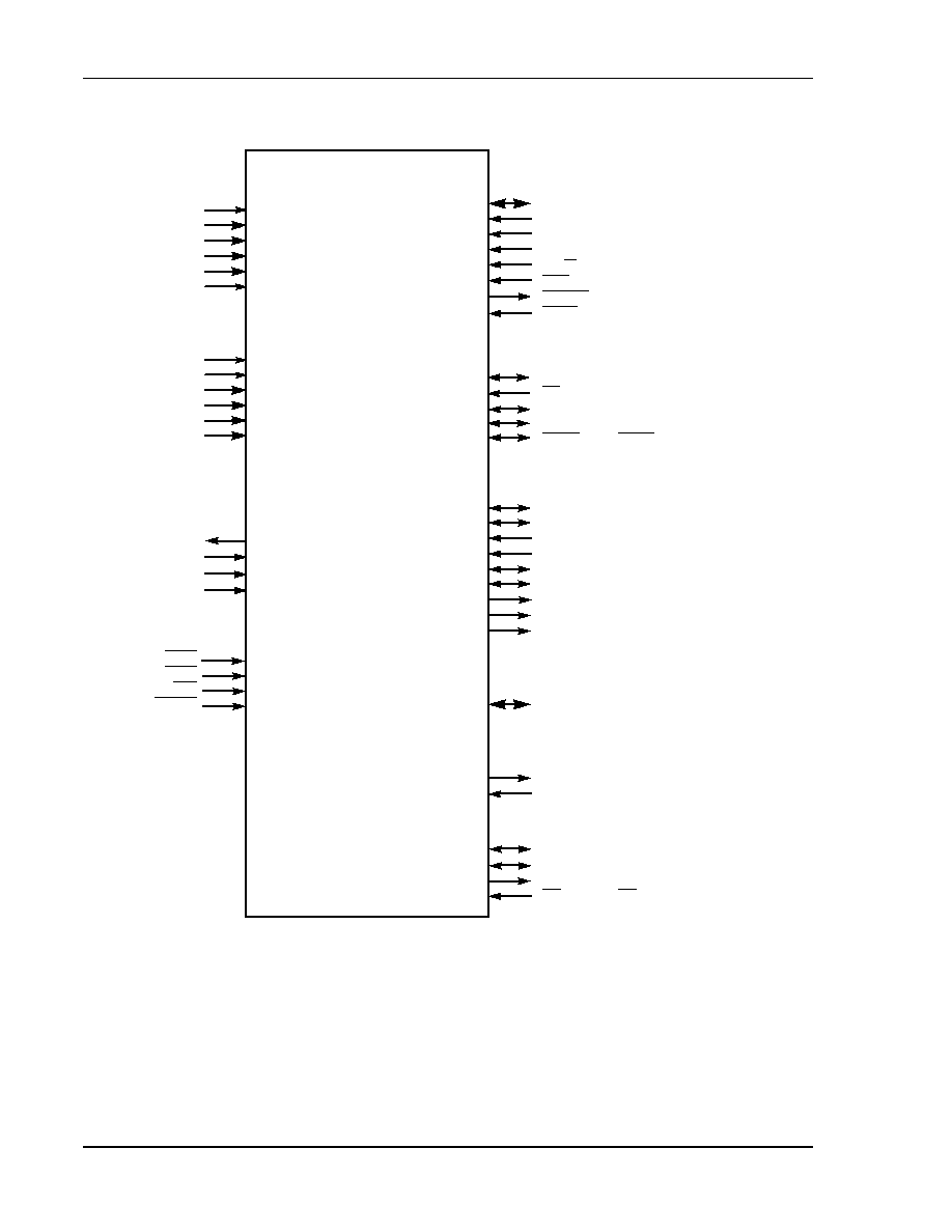
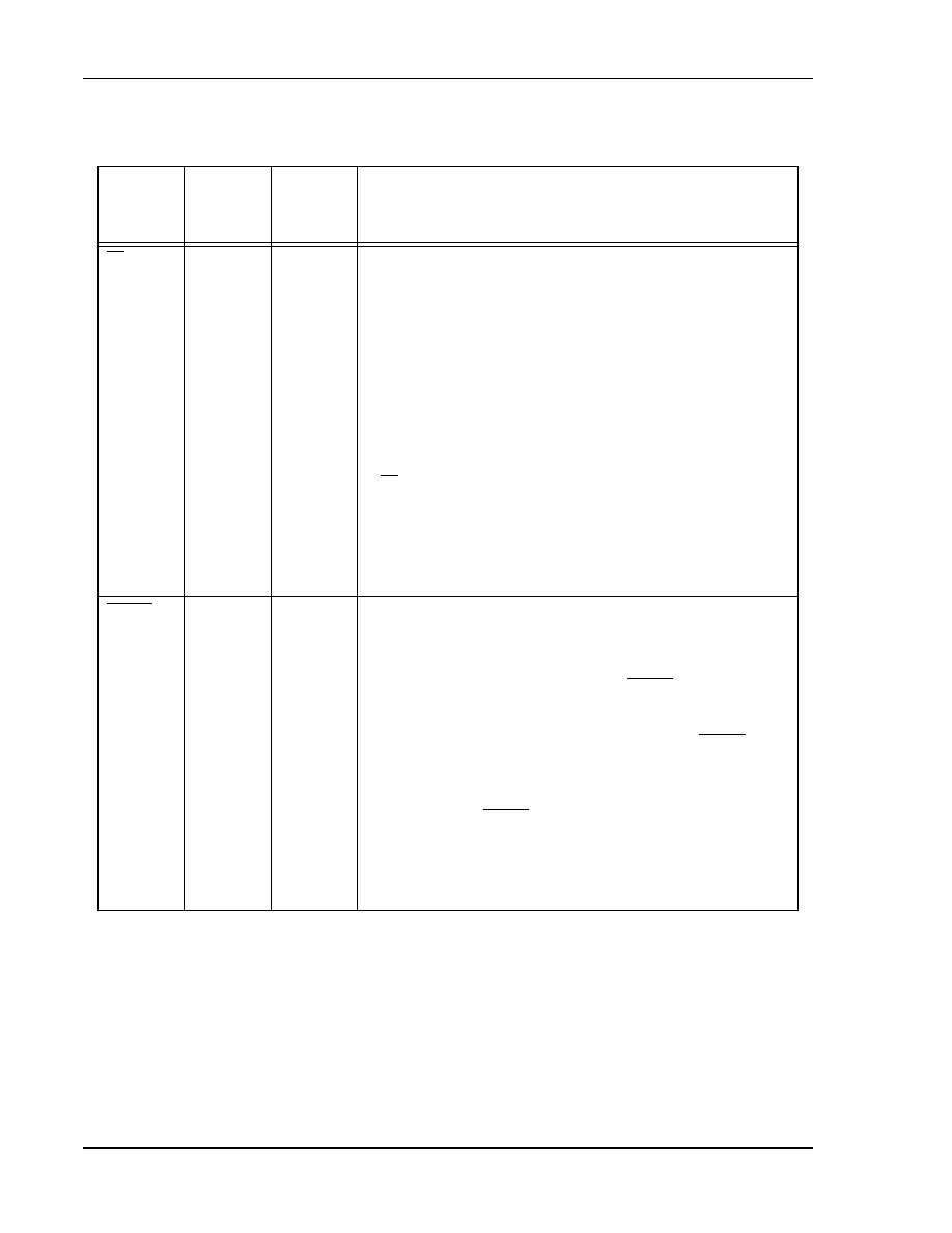
Figure 1
shows the functional blocks of the DSP56011.
Figure 1
DSP56011 Block Diagram
Y Data
Memory
X Data
Memory
Program
Memory
Program Control Unit
24-Bit
DSP56000
Core
OnCE
TM
Port
PLL
Clock
Gen.
8
9
5
2
16-Bit Bus
24-Bit Bus
Data ALU
24
�
24 + 56
56-Bit MAC
Two 56-Bit Accumulators
4
IRQA, IRQB, NMI, RESET
4
3
Internal
Data
Bus
Switch
Address
Generation
Unit
PAB
XAB
YAB
GDB
PDB
XDB
YDB
General
Purpose
I/O
(GPIO)
Digital
Audio
Transmitter
(DAX)
Serial
Audio
Interface
(SAI)
Serial
Host
Interface
(SHI)
Parallel
Host
Interface
(HI)
15
EXTAL
Expansion
Area
Program
Address
Generator
Program
Decode
Controller
Program
Interrupt
Controller
AA1271
Rev. 1

Preliminary Information
ii
DSP56011 Technical Data Sheet, Rev. 1
MOTOROLA
DSP56011
PRELIMINARY
TABLE OF CONTENTS
SECTION 1
SIGNAL/CONNECTION DESCRIPTIONS . . . . . . . . . . . . . . . . . . 1-1
SECTION 2
SPECIFICATIONS . . . . . . . . . . . . . . . . . . . . . . . . . . . . . . . . . . . . 2-1
SECTION 3
PACKAGING . . . . . . . . . . . . . . . . . . . . . . . . . . . . . . . . . . . . . . . . 3-1
SECTION 4
DESIGN CONSIDERATIONS . . . . . . . . . . . . . . . . . . . . . . . . . . . 4-1
SECTION 5
ORDERING INFORMATION . . . . . . . . . . . . . . . . . . . . . . . . . . . . 5-1
FOR TECHNICAL ASSISTANCE:
Telephone:
1-800-521-6274
Email:
dsphelp@dsp.sps.mot.com
Internet:
http://www.motorola-dsp.com
Data Sheet Conventions
This data sheet uses the following conventions:
OVERBAR
Used to indicate a signal that is active when pulled low (For example, the RESET
pin is active when low.)
"asserted"
Means that a high true (active high) signal is high or that a low true (active low)
signal is low
"deasserted"
Means that a high true (active high) signal is low or that a low true (active low)
signal is high
Examples:
Signal/Symbol
Logic State
Signal State
Voltage
PIN
True
Asserted
V
IL
/V
OL
PIN
False
Deasserted
V
IH
/V
OH
PIN
True
Asserted
V
IH
/V
OH
PIN
False
Deasserted
V
IL
/V
OL
Note:
Values for V
IL
, V
OL
, V
IH
, and V
OH
are defined by individual product specifications.

DSP56011
Features
Preliminary Information
MOTOROLA
DSP56011 Technical Data Sheet, Rev. 1
iii
PRELIMINARY
FEATURES
Digital Signal Processing Core
�
Efficient, object-code compatible, 24-bit DSP56000 family DSP engine
�
47.5 Million Instructions Per Second (MIPS) with 21.05 ns instruction cycle at 95 MHz
�
Highly parallel instruction set with unique DSP addressing modes
�
Two 56-bit accumulators including extension byte
�
Parallel 24
�
24-bit multiply-accumulate in 1 instruction cycle (2 clock cycles)
�
Double precision 48
�
48-bit multiply with 96-bit result in 6 instruction cycles
�
56-bit addition/subtraction in 1 instruction cycle
�
Fractional and integer arithmetic with support for multi-precision arithmetic
�
Hardware support for block-floating point Fast Fourier Transforms (FFT)
�
Hardware nested DO loops
�
Zero-overhead fast interrupts (2 instruction cycles)
�
PLL-based clocking with a wide range of frequency multiplications (1 to 4096) and
power saving clock divider (2
i
: i = 0 to 15), which reduces clock noise
�
Four 24-bit internal data buses and three 16-bit internal address buses for
simultaneous accesses to one program and two data memories

Preliminary Information
iv
DSP56011 Technical Data Sheet, Rev. 1
MOTOROLA
DSP56011
Features
PRELIMINARY
Memory
�
Modified Harvard architecture allows simultaneous access to program and data
memories
�
12800
�
24-bit on-chip Program ROM
1
�
4096
�
24-bit on-chip X-data RAM and 3584
�
24-bit on-chip X-data ROM
1
�
4352
�
24-bit on-chip Y-data RAM and 2048
�
24-bit on-chip Y-data ROM
1
�
512
�
24-bit on-chip Program RAM and 64
�
24-bit bootstrap ROM
�
As much as 2304
�
24 bits of X- and Y-data RAM can be switched to Program RAM,
giving a total of 2816
�
24 bits of Program RAM
Table 1
lists the memory configurations of the DSP56011.
1.These ROMs may be factory programmed with data/program provided by the application developer.
Table 1
DSP56011 Internal Memory Configurations
Memory Type
No Switch
(PEA = 0, PEB = 0)
Switch A
(PEA = 1, PEB = 0)
Switch B
(PEA = 0, PEB = 1)
Switch A+B
(PEA = 1, PEB = 1)
Program RAM
0.5 K
1.25 K
2.0 K
2.75 K
X data RAM
4.0 K
3.25 K
3.25 K
2.5 K
Y data RAM
4.25 K
4.25 K
3.5 K
3.5 K
Program ROM
12.5 K
12.5 K
12.5 K
12.5 K
X data ROM
3.5 K
3.5 K
3.5 K
3.5 K
Y data ROM
2.0 K
2.0 K
2.0 K
2.0 K

DSP56011
Features
Preliminary Information
MOTOROLA
DSP56011 Technical Data Sheet, Rev. 1
v
PRELIMINARY
Peripheral and Support Circuits
�
SAI includes:
�
Two receivers and three transmitters
�
Master or slave capability
�
I
2
S, Sony, and Matshushita audio protocol implementations
�
Two sets of SAI interrupt vectors
�
SHI features:
�
Single master capability
�
SPI and I
2
C protocols
�
10-word receive FIFO
�
Support for 8-, 16- and 24-bit words.
�
Byte-wide Parallel Host Interface with DMA support capable of reconfiguration as fifteen
General Purpose Input/Output (GPIO) lines
�
DAX features one serial transmitter capable of supporting S/PDIF, IEC958, CP-340, and
AES/EBU formats.
�
Eight dedicated, independent, programmable GPIO lines
�
On-chip peripheral registers memory mapped in data memory space
�
OnCE port for unobtrusive, processor speed-independent debugging
�
Software programmable PLL-based frequency synthesizer for the core clock
�
Power saving Wait and Stop modes
�
Fully static, HCMOS design from specified operating frequency down to dc
�
100-pin plastic Thin Quad Flat Pack (TQFP) surface-mount package
�
5 V power supply

Preliminary Information
vi
DSP56011 Technical Data Sheet, Rev. 1
MOTOROLA
DSP56011
Documentation
PRELIMINARY
DOCUMENTATION
Table 2
lists the documents that provide a complete description of the DSP56011 and are
required to design properly with the part. Documentation is available from a local Motorola
distributor, a Motorola semiconductor sales office, a Motorola Literature Distribution Center, or
through the Motorola DSP home page on the Internet (the source for the latest information).
Table 2
Additional DSP56011 Documentation
Document Name
Description
Order Number
DSP56000 Family
Manual
Detailed description of the 56000-family architecture
and the 24-bit core processor and instruction set
DSP56KFAMUM/AD
DSP56011 User's
Manual
Detailed description of memory, peripherals, and
interfaces
DSP56011UM/AD
DSP56011
Technical Data
Electrical and timing specifications, and pin and
package descriptions
DSP56011/D

Preliminary Information
MOTOROLA
DSP56011 Technical Data Sheet, Rev. 1
1-1
PRELIMINARY
SECTION
1
SIGNAL/CONNECTION DESCRIPTIONS
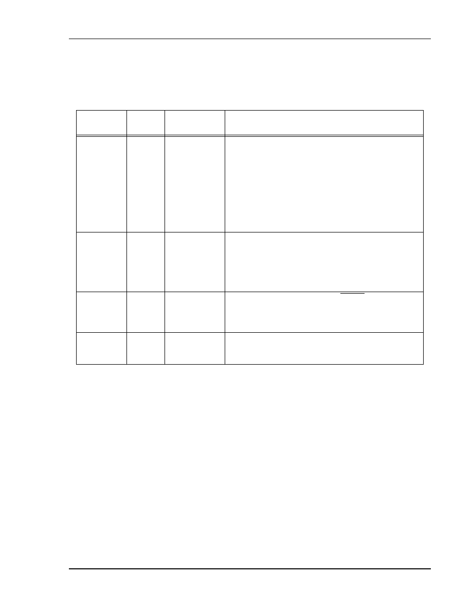
SIGNAL GROUPINGS
The input and output signals of the DSP56011 are organized into ten functional
groups, as shown in
Table 1-1
and as illustrated in
Figure 1-1
.
Figure 1-1
is a diagram of DSP56011 signals by functional group.
Table 1-1
DSP56011 Functional Signal Groupings
Functional Group
Number of
Signals
Detailed
Description
Power (V
CC
)
13
Table 1-2
Ground (GND)
17
Table 1-3
PLL
4
Table 1-4
Interrupt and Mode Control
4
Table 1-5
Host Interface (HI)
Port B
15
Table 1-6
Serial Host Interface (SHI)
5
Table 1-7
Serial Audio Interface (SAI)
9
Table 1-8
Table 1-9
General Purpose Input/Output (GPIO)
8
Table 1-10
Digital Audio Transmitter (DAX)
2
Table 1-11
OnCE Port
4
Table 1-12
Preliminary Information
1-2
DSP56011 Technical Data Sheet, Rev. 1
MOTOROLA
Signal/Connection Descriptions
Signal Groupings
PRELIMINARY
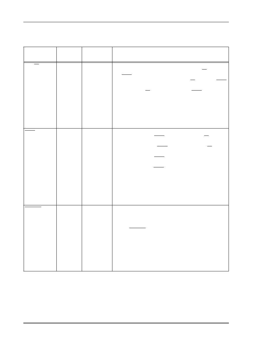
Figure 1-1 Signals Identified by Functional Group
DSP56011
Digital Audio
Transmitter (DAX)
PLL
OnCETM
Port
Power Inputs:
PLL
Internal Logic
A
D
HI
SHI
Debug
DSI
DSCK
DSO
DR
PLOCK
PCAP
PINIT
EXTAL
V
CCP
V
CCQ
V
CCA
V
CCD
V
CCH
V
CCS
4
Serial Audio
Interface (SAI)
Rec0
Rec1
Tran0
Tran1
Tran2
1
2
3
Grounds:
PLL
Internal Logic
A
D
HI
SHI
GND
P
GND
Q
GND
A
GND
D
GND
H
GND
S
4
3
2
3
Interrupt/
Mode
Control
MODA/IRQA
MODB/IRQB
MODC/NMI
RESET
Host
Interface
(HI) Port
H0�H7
HOA0
HOA1
HOA2
HR/W
HEN
HOREQ
HACK
WSR
SCKR
SDI0
SDI1
WST
SCKT
SDO0
SDO1
SDO2
ADO
ACI
8
2
4
Serial Host
Interface (SHI)
SPI Mode
MOSI
SS
MISO
SCK
HREQ
Port B GPIO
PB0�PB7
PB8
PB9
PB10
PB11
PB12
PB13
PB14
General Purpose
Input/Output (GPIO)
GPIO0�GPIO7
8
HI
I
2
C Mode
HA0
HA2
SDA
SCL
HREQ
Non-Debug
OS0
OS1
DSO
DR

Preliminary Information
MOTOROLA
DSP56011 Technical Data Sheet, Rev. 1
1-3
Signal/Connection Descriptions
Power
PRELIMINARY
POWER
Table 1-2
Power Inputs
Power Name
Description
V
CCP
PLL Power
--V
CCP
is V
CC
dedicated for Phase Lock Loop (PLL) use. The voltage
should be well-regulated and the input should be provided with an extremely
low impedance path to the V
CC
power rail. V
CCP
should be bypassed to GND
P
by a 0.1
�
F capacitor located as close as possible to the chip package.
V
CCQ
Quiet Power
--V
CCQ
is an isolated power for the internal processing logic. This
input must be tied externally to all other chip power inputs. The user must
provide adequate external decoupling capacitors.
V
CCA
A Power
--V
CCA
is an isolated power for sections of the internal chip logic. This
input must be tied externally to all other chip power inputs. The user must
provide adequate external decoupling capacitors.
V
CCD
D Power
--V
CCD
is an isolated power for sections of the internal chip logic. This
input must be tied externally to all other chip power inputs. The user must
provide adequate external decoupling capacitors.
V
CCH
Host Power
--V
CCH
is an isolated power for the HI I/O drivers. This input must
be tied externally to all other chip power inputs. The user must provide adequate
external decoupling capacitors.
V
CCS
Serial Host Power
--V
CCS
is an isolated power for the SHI I/O drivers. This
input must be tied externally to all other chip power inputs. The user must
provide adequate external decoupling capacitors.

Preliminary Information
1-4
DSP56011 Technical Data Sheet, Rev. 1
MOTOROLA
Signal/Connection Descriptions
Ground
PRELIMINARY
GROUND
Table 1-3
Grounds
Ground Name
Description
GND
P
PLL Ground
--GND
P
is ground dedicated for PLL use. The connection should be
provided with an extremely low-impedance path to ground. V
CCP
should be
bypassed to GND
P
by a 0.1
�
F capacitor located as close as possible to the chip
package.
GND
Q
Internal Logic Ground
--GND
Q
is an isolated ground for the internal processing
logic. This connection must be tied externally to all other chip ground
connections. The user must provide adequate external decoupling capacitors.
GND
A
A Ground
--GND
A
is an isolated ground for sections of the internal logic. This
connection must be tied externally to all other chip ground connections. The user
must provide adequate external decoupling capacitors.
GND
D
D Ground
--GND
D
is an isolated ground for sections of the internal logic. This
connection must be tied externally to all other chip ground connections. The user
must provide adequate external decoupling capacitors.
GND
H
Host Ground
--GND
H
is an isolated ground for the HI I/O drivers. This
connection must be tied externally to all other chip ground connections. The user
must provide adequate external decoupling capacitors.
GND
S
Serial Host Ground
--GND
S
is an isolated ground for the SHI I/O drivers. This
connection must be tied externally to all other chip ground connections. The user
must provide adequate external decoupling capacitors.
Preliminary Information
MOTOROLA
DSP56011 Technical Data Sheet, Rev. 1
1-5
Signal/Connection Descriptions
Phase Lock Loop (PLL)
PRELIMINARY
PHASE LOCK LOOP (PLL)
Table 1-4
Phase Lock Loop Signals
Signal Name
Type
State During
Reset
Signal Description
PLOCK
Output
Indeterminate
Phase Locked
--PLOCK is an output signal that, when
driven high, indicates that the PLL has achieved phase
lock. After Reset, PLOCK is driven low until lock is
achieved.
Note:
PLOCK is a reliable indicator of the PLL lock
state only after the chip has exited the Reset
state. During hardware reset, the PLOCK state is
determined by PINIT and the current PLL lock
condition.
PCAP
Input
Input
PLL Capacitor
--PCAP is an input connecting an off-chip
capacitor to the PLL filter. Connect one capacitor
terminal to PCAP and the other terminal to V
CCP
.
If the PLL is not used, PCAP may be tied to V
CC
, GND,
or left floating.
PINIT
Input
Input
PLL Initial
--During assertion of RESET, the value of
PINIT is written into the PLL Enable (PEN) bit of the PLL
Control Register, determining whether the PLL is
enabled or disabled.
EXTAL
Input
Input
External Clock/Crystal Input
--EXTAL interfaces the
internal crystal oscillator input to an external crystal or
an external clock.

Preliminary Information
1-6
DSP56011 Technical Data Sheet, Rev. 1
MOTOROLA
Signal/Connection Descriptions
Interrupt and Mode Control
PRELIMINARY
INTERRUPT AND MODE CONTROL
Table 1-5
Interrupt and Mode Control
Signal
Name
Type
State During
Reset
Signal Description
MODA
IRQA
Input
Input
Input (MODA) Mode Select A--This input signal has three functions:
�
to work with the MODB and MODC signals to
select the DSP's initial operating mode,
�
to allow an external device to request a DSP
interrupt after internal synchronization, and
�
to turn on the internal clock generator when the
DSP is in the Stop processing state, causing the DSP
to resume processing.
MODA is read and internally latched in the DSP when the
processor exits the Reset state. The logic state present on the
MODA, MODB, and MODC pins selects the initial DSP
operating mode. Several clock cycles after leaving the Reset
state, the MODA signal changes to the external interrupt
request IRQA. The DSP operating mode can be changed by
software after reset.
External Interrupt Request A (IRQA)
--The IRQA input is a
synchronized external interrupt request. It may be
programmed to be level-sensitive or negative-edge
triggered. When the signal is edge-triggered, triggering
occurs at a voltage level and is not directly related to the fall
time of the interrupt signal. However, as the fall time of the
interrupt signal increases, the probability that noise on
IRQA will generate multiple interrupts also increases.
While the DSP is in the Stop mode, asserting IRQA gates on
the oscillator and, after a clock stabilization delay, enables
clocks to the processor and peripherals. Hardware reset
causes this input to function as MODA.

Preliminary Information
MOTOROLA
DSP56011 Technical Data Sheet, Rev. 1
1-7
Signal/Connection Descriptions
Interrupt and Mode Control
PRELIMINARY
MODB
IRQB
Input
Input
Input (MODB) Mode Select B--This input signal has two functions:
�
to work with the MODA and MODC signals to
select the DSP's initial operating mode, and
�
to allow an external device to request a DSP
interrupt after internal synchronization.
MODB is read and internally latched in the DSP when the
processor exits the Reset state. The logic state present on the
MODA, MODB, and MODC pins selects the initial DSP
operating mode. Several clock cycles after leaving the Reset
state, the MODB signal changes to the external interrupt
request IRQB. The DSP operating mode can be changed by
software after reset.
External Interrupt Request
B (IRQB)--The IRQB input is a
synchronized external interrupt request. It may be
programmed to be level-sensitive or negative-edge
triggered. When the signal is edge-triggered, triggering
occurs at a voltage level and is not directly related to the fall
time of the interrupt signal. However, as the fall time of the
interrupt signal increases, the probability that noise on IRQB
will generate multiple interrupts also increases. Hardware
reset causes this input to function as MODB.
Table 1-5
Interrupt and Mode Control (Continued)
Signal
Name
Type
State During
Reset
Signal Description

Preliminary Information
1-8
DSP56011 Technical Data Sheet, Rev. 1
MOTOROLA
Signal/Connection Descriptions
Interrupt and Mode Control
PRELIMINARY
MODC
NMI
Input, edge-
triggered
Input, edge-
triggered
Input (MODC) Mode Select C--This input signal has two functions:
�
to work with the MODA and MODB signals to
select the DSP's initial operating mode, and
�
to allow an external device to request a DSP
interrupt after internal synchronization.
MODC is read and internally latched in the DSP when the
processor exits the Reset state. The logic state present on the
MODA, MODB, and MODC pins selects the initial DSP
operating mode. Several clock cycles after leaving the Reset
state, the MODC signal changes to the Non-Maskable
Interrupt request, NMI. The DSP operating mode can be
changed by software after reset.
Non-Maskable Interrupt Request
--The NMI input is a
negative-edge triggered external interrupt request. This is a
level 3 interrupt that can not be masked out. Triggering
occurs at a voltage level and is not directly related to the fall
time of the interrupt signal. However, as the fall time of the
interrupt signal increases, the probability that noise on NMI
will generate multiple interrupts also increases. Hardware
reset causes this input to function as MODC.
RESET
Input
Active
Reset--This input causes a direct hardware reset of the
processor. When RESET is asserted, the DSP is initialized and
placed in the Reset state. A Schmitt-trigger input is used for
noise immunity. When the reset signal is deasserted, the initial
DSP operating mode is latched from the MODA, MODB, and
MODC signals. The DSP also samples the PINIT signal and
writes its status into the PEN bit of the PLL Control Register.
When the DSP comes out of the Reset state, deassertion
occurs at a voltage level and is not directly related to the rise
time of the RESET signal. However, the probability that
noise on RESET will generate multiple resets increases with
increasing rise time of the RESET signal.
For proper hardware reset to occur, the clock must be active,
since a number of clock ticks are required for proper
propagation of the hardware Reset state.
Table 1-5
Interrupt and Mode Control (Continued)
Signal
Name
Type
State During
Reset
Signal Description

Preliminary Information
MOTOROLA
DSP56011 Technical Data Sheet, Rev. 1
1-9
Signal/Connection Descriptions
Host Interface (HI)
PRELIMINARY
HOST INTERFACE (HI)
The HI provides a fast parallel data to 8-bit port, which may be connected directly to
the host bus. The HI supports a variety of standard buses, and can be directly
connected to a number of industry standard microcomputers, microprocessors, DSPs,
and DMA hardware.
Table 1-6
Host Interface
Signal Name
Type
State During
Reset
Signal Description
H0�H7
PB0�PB7
Input/
Output
Input
Host Data Bus (H0�H7)
--This data bus transfers data
between the host processor and the DSP56011.
When configured as a Host Interface port, the H0�H7
signals are tri-stated as long as HEN is deasserted. The
signals are inputs unless HR/W is high and HEN is
asserted, in which case H0�H7 become outputs, allowing
the host processor to read the DSP56011 data. H0�H7
become outputs when HACK is asserted during HOREQ
assertion.
Port B GPIO 0�7 (PB0�PB7)
--These signals are General
Purpose I/O signals (PB0�PB7) when the Host Interface is
not selected.
After reset, the default state for these signals is GPIO input.
HOA0�HOA2
PB8�PB10
Input
Input/
Output
Input
Host Address0�Host Address 2 (HOA0�HOA2)
--These
inputs provide the address selection for each Host
Interface register.
Port B GPIO 8�10 (PB8�PB10)
--These signals are General
Purpose I/O signals (PB8�PB10) when the Host Interface is
not selected.
After reset, the default state for these signals is GPIO
input.
Preliminary Information
1-10
DSP56011 Technical Data Sheet, Rev. 1
MOTOROLA
Signal/Connection Descriptions
Host Interface (HI)
PRELIMINARY
HR/W
PB11
Input
Input/
Output
Input
Host Read/Write
--This input selects the direction of data
transfer for each host processor access. If HR/W is high
and HEN is asserted, H0�H7 are outputs and DSP data is
transferred to the host processor. If HR/W is low and HEN
is asserted, H0�H7 are inputs and host data is transferred
to the DSP. HR/W must be stable when HEN is asserted.
Port B GPIO 11 (PB11)
--This signal is a General Purpose
I/O signal (PB11) when the Host Interface is not being
used.
After reset, the default state for this signal is GPIO input.
HEN
PB12
Input
Input/
Output
Input
Host Enable
--This input enables a data transfer on the
host data bus. When HEN is asserted and HR/W is high,
H0�H7 become outputs and the host processor may read
DSP56011 data. When HEN is asserted and HR/W is low,
H0�H7 become inputs. Host data is latched inside the DSP
on the rising edge of HEN. Normally, a chip select signal
derived from host address decoding and an enable strobe
are used to generate HEN.
Port B GPIO 12 (PB12)
--This signal is a General Purpose
I/O signal (PB12) when the Host Interface is not being
used.
After reset, the default state for this signal is GPIO input.
HOREQ
PB13
Open-
drain
Output
Input/
Output
Input
Host Request
--This signal is used by the Host Interface to
request service from the host processor, DMA controller,
or a simple external controller.
Note:
HOREQ should always be pulled high when it is
not in use.
Port B GPIO 13 (PB13)
--This signal is a General Purpose
(not open-drain) I/O signal (PB13) when the Host
Interface is not selected.
After reset, the default state for this signal is GPIO input.
Table 1-6
Host Interface (Continued)
Signal Name
Type
State During
Reset
Signal Description

Preliminary Information
MOTOROLA
DSP56011 Technical Data Sheet, Rev. 1
1-11
Signal/Connection Descriptions
Host Interface (HI)
PRELIMINARY
HACK
PB14
Input
Input/
Output
Input
Host Acknowledge
--This input has two functions. It
provides a host acknowledge handshake signal for DMA
transfers and it receives a host interrupt acknowledge
compatible with MC68000 Family processors.
Note:
HACK should always be pulled high when it is
not in use.
Port B GPIO 14 (PB14)
--This signal is a General Purpose
I/O signal (PB14) when the Host Interface is not selected.
After reset, the default state for this signal is GPIO input.
Table 1-6
Host Interface (Continued)
Signal Name
Type
State During
Reset
Signal Description

Preliminary Information
1-12
DSP56011 Technical Data Sheet, Rev. 1
MOTOROLA
Signal/Connection Descriptions
Serial Host Interface (SHI)
PRELIMINARY
SERIAL HOST INTERFACE (SHI)
The SHI has five I/O signals that can be configured to allow the SHI to operate in
either SPI or I
2
C mode.
Table 1-7
Serial Host Interface (SHI) Signals
Signal
Name
Signal
Type
State
during
Reset
Signal Description
SCK
SCL
Input or
Output
Input or
Output
Tri-stated
SPI Serial Clock
--The SCK signal is an output when the SPI
is configured as a master, and a Schmitt-trigger input when
the SPI is configured as a slave. When the SPI is configured as
a master, the SCK signal is derived from the internal SHI
clock generator. When the SPI is configured as a slave, the
SCK signal is an input, and the clock signal from the external
master synchronizes the data transfer. The SCK signal is
ignored by the SPI if it is defined as a slave and the Slave
Select (SS) signal is not asserted. In both the master and slave
SPI devices, data is shifted on one edge of the SCK signal and
is sampled on the opposite edge where data is stable. Edge
polarity is determined by the SPI transfer protocol. The
maximum allowed internally generated bit clock frequency is
f
osc
/4 for the SPI mode, where f
osc
is the clock on EXTAL.
The maximum allowed externally generated bit clock
frequency is f
osc
/3 for the SPI mode.
I
2
C Serial Clock
--SCL carries the clock for I
2
C bus
transactions in the I
2
C mode. SCL is a Schmitt-trigger input
when configured as a slave, and an open-drain output when
configured as a master. SCL should be connected to V
CC
through a pull-up resistor. The maximum allowed internally
generated bit clock frequency is f
osc
/6 for the I
2
C mode
where f
osc
is the clock on EXTAL. The maximum allowed
externally generated bit clock frequency is f
osc
/5 for the I
2
C
mode.
An external pull-up resistor is not required.
Preliminary Information
MOTOROLA
DSP56011 Technical Data Sheet, Rev. 1
1-13
Signal/Connection Descriptions
Serial Host Interface (SHI)
PRELIMINARY
MISO
SDA
Input or
Output
Input or
open-
drain
Output
Tri-stated
SPI Master-In-Slave-Out
--When the SPI is configured as a
master, MISO is the master data input line. The MISO signal
is used in conjunction with the MOSI signal for transmitting
and receiving serial data. This signal is a Schmitt-trigger
input when configured for the SPI Master mode, an output
when configured for the SPI Slave mode, and tri-stated if
configured for the SPI Slave mode when SS is deasserted. An
external pull-up resistor is not required for SPI operation.
I
2
C Data and Acknowledge
--In I
2
C mode, SDA is a Schmitt-
trigger input when receiving and an open-drain output when
transmitting. SDA should be connected to V
CC
through a
pull-up resistor. SDA carries the data for I
2
C transactions.
The data in SDA must be stable during the high period of
SCL. The data in SDA is only allowed to change when SCL is
low. When the bus is free, SDA is high. The SDA line is only
allowed to change during the time SCL is high in the case of
start and stop events. A high to low transition of the SDA line
while SCL is high is an unique situation, which is defined as
the start event. A low to high transition of SDA while SCL is
high is an unique situation, which is defined as the stop
event.
MOSI
HA0
Input or
Output
Input
Tri-stated
SPI Master-Out-Slave-In
--When the SPI is configured as a
master, MOSI is the master data output line. The MOSI signal
is used in conjunction with the MISO signal for transmitting
and receiving serial data. MOSI is the slave data input line
when the SPI is configured as a slave. This signal is a Schmitt-
trigger input when configured for the SPI Slave mode.
I
2
C Slave Address 0
--This signal uses a Schmitt-trigger
input when configured for the I
2
C mode. When configured
for I
2
C Slave mode, the HA0 signal is used to form the slave
device address. HA0 is ignored when it is configured for the
I
2
C Master mode.
An external pull-up resistor is not required.
Table 1-7
Serial Host Interface (SHI) Signals (Continued)
Signal
Name
Signal
Type
State
during
Reset
Signal Description
Preliminary Information
1-14
DSP56011 Technical Data Sheet, Rev. 1
MOTOROLA
Signal/Connection Descriptions
Serial Host Interface (SHI)
PRELIMINARY
SS
HA2
Input
Input
Tri-stated
SPI Slave Select
--This signal is an active low Schmitt-trigger
input when configured for the SPI mode. When configured
for the SPI Slave mode, this signal is used to enable the SPI
slave for transfer. When configured for the SPI Master mode,
this signal should be kept deasserted (pulled high). If it is
asserted while configured as SPI master, a bus error
condition is flagged.
I
2
C Slave Address 2
--This signal uses a Schmitt-trigger
input when configured for the I
2
C mode. When configured
for the I
2
C Slave mode, the HA2 signal is used to form the
slave device address. HA2 is ignored in the I
2
C Master mode.
If SS is deasserted, the SHI ignores SCK clocks and keeps the
MISO output signal in the high-impedance state.
This signal is tri-stated during hardware, software, or
individual reset (thus, there is no need for an external pull-up
in this state).
HREQ
Input or
Output
Tri-stated
Host Request
--This signal is an active low Schmitt-trigger
input when configured for the Master mode, but an active
low output when configured for the Slave mode.
When configured for the Slave mode, HREQ is asserted to
indicate that the SHI is ready for the next data word transfer
and deasserted at the first clock pulse of the new data word
transfer. When configured for the Master mode, HREQ is an
input and when asserted by the external slave device, it will
trigger the start of the data word transfer by the master. After
finishing the data word transfer, the master will await the
next assertion of HREQ to proceed to the next transfer.
This signal is tri-stated during hardware, software, personal
reset, or when the HREQ1�HREQ0 bits in the HCSR are
cleared (no need for external pull-up in this state).
Table 1-7
Serial Host Interface (SHI) Signals (Continued)
Signal
Name
Signal
Type
State
during
Reset
Signal Description

Preliminary Information
MOTOROLA
DSP56011 Technical Data Sheet, Rev. 1
1-15
Signal/Connection Descriptions
Serial Audio Interface (SAI)
PRELIMINARY
SERIAL AUDIO INTERFACE (SAI)
The SAI is composed of separate receiver and transmitter sections.
SAI Receive Section
The receive section of the SAI has four dedicated signals
.
Table 1-8
Serial Audio Interface (SAI) Receive Signals
Signal
Name
Signal
Type
State
during
Reset
Signal Description
SDI0
Input
Tri-
stated
Serial Data Input 0
--This is the receiver 0 serial data input.
This signal is high impedance during hardware or software
reset, while receiver 0 is disabled (R0EN = 0), or while the chip
is in the Stop state. No external pull-up resistor is required.
SDI1
Input
Tri-
stated
Serial Data Input 1
--This is the receiver 1 serial data input.
This signal is high impedance during hardware or software
reset, while receiver 1 is disabled (R1EN = 0), or while the chip
is in the Stop state. No external pull-up resistor is required.
SCKR
Input or
Output
Tri-
stated
Receive Serial Clock
--SCKR is an output if the receiver
section is programmed as a master, and a Schmitt-trigger
input if programmed as a slave.
SCKR is high impedance if all receivers are disabled (personal
reset) and during hardware or software reset, or while the chip
is in the Stop state. No external pull-up is necessary.
WSR
Input or
Output
Tri-
stated
Receive Word Select
--WSR is an output if the receiver section
is programmed as a master, and a Schmitt-trigger input if
programmed as a slave. WSR is used to synchronize the data
word and to select the left/right portion of the data sample.
WSR is high impedance if all receivers are disabled (personal
reset), during hardware reset, during software reset, or while
the chip is in the stop state. No external pull-up is necessary.
Preliminary Information
1-16
DSP56011 Technical Data Sheet, Rev. 1
MOTOROLA
Signal/Connection Descriptions
Serial Audio Interface (SAI)
PRELIMINARY
SAI Transmit Section
The transmit section of the SAI has five dedicated signals.
Table 1-9
Serial Audio Interface (SAI) Transmit Signals
Signal
Name
Signal
Type
State
during
Reset
Signal Description
SDO0
Output
Driven
high
Serial Data Output 0
--SDO0 is the transmitter 0 serial output.
SDO0 is driven high if transmitter 0 is disabled, during
personal reset, hardware reset and software reset, or when the
chip is in the Stop state.
SDO1
Output
Driven
high
Serial Data Output 1
--SDO1 is the transmitter 1 serial output.
SDO1 is driven high if transmitter 1 is disabled, during
personal reset, hardware reset and software reset, or when the
chip is in the Stop state.
SDO2
Output
Driven
high
Serial Data Output 2
--SDO2 is the transmitter 2 serial output.
SDO2 is driven high if transmitter 2 is disabled, during
personal reset, hardware reset and software reset, or when the
chip is in the Stop state.
SCKT
Input
or
Output
Tri-
stated
Transmit Serial Clock
--This signal provides the clock for the
Serial Audio Interface (SAI). The SCKT signal can be an output
if the transmit section is programmed as a master, or a Schmitt-
trigger input if the transmit section is programmed as a slave.
When the SCKT is an output, it provides an internally
generated SAI transmit clock to external circuitry. When the
SCKT is an input, it allows external circuitry to clock data out
of the SAI.
SCKT is tri-stated if all transmitters are disabled (personal
reset), during hardware reset, software reset, or while the chip
is in the Stop state. No external pull-up is necessary.
WST
Input
or
Output
Tri-
stated
Transmit Word Select
--WST is an output if the transmit
section is programmed as a master, and a Schmitt-trigger input
if programmed as a slave. WST is used to synchronize the data
word and select the left/right portion of the data sample.
WST is tri-stated if all transmitters are disabled (personal reset),
during hardware or software reset, or while the chip is in the
Stop state. No external pull-up is necessary.

Preliminary Information
MOTOROLA
DSP56011 Technical Data Sheet, Rev. 1
1-17
Signal/Connection Descriptions
General Purpose Input/Output (GPIO)
PRELIMINARY
GENERAL PURPOSE INPUT/OUTPUT (GPIO)
DIGITAL AUDIO INTERFACE (DAX)
Table 1-10
General Purpose I/O (GPIO) Signals
Signal
Name
Signal Type
State during
Reset
Signal Description
GPIO0�
GPIO7
Input or
Output
(standard or
open-drain)
Disconnected
internally
General Purpose Input/Output
--These signals
are used for control and handshake functions
between the DSP and external circuitry. Each
GPIO signal may be individually programmed to
be one of four states:
�
Not connected
�
Input
�
Standard output
�
Open-drain output
Table 1-11
Digital Audio Interface (DAX) Signals
Signal Name
Type
State During
Reset
Signal Description
ADO
Output
Output, driven
high
Digital Audio Data Output
--This signal is an
audio and non-audio output in the form of AES/
EBU, CP340 and IEC958 data in a biphase mark
format. The signal is driven high when the DAX is
disabled, and during hardware or software reset.
ACI
Input
Tri-stated
Audio Clock Input
--This is the DAX clock input.
When programmed to use an external clock, this
input supplies the DAX clock. The external clock
frequency must 256, 384, or 512 times the audio
sampling frequency (256 x Fs, 384 x Fs or 512 x Fs,
respectively). The ACI signal is high impedance
(tri-stated) only during hardware or software reset.
If the DAX is not used, connect the ACI signal to
ground through an external pull-down resistor to
ensure a stable logic level at the input.

Preliminary Information
1-18
DSP56011 Technical Data Sheet, Rev. 1
MOTOROLA
Signal/Connection Descriptions
OnCE Port
PRELIMINARY
OnCE PORT
Table 1-12
On-Chip Emulation Port (OnCE) Signals
Signal
Name
Signal
Type
State
during
Reset
Signal Description
DSI
OS0
Input
Output
Low
Output
Debug Serial Input
--In Debug mode, serial data or
commands are provided as inputs to the OnCE controller via
the DSI signal. Data is latched on the falling edge of the DSCK
serial clock. Data is always shifted into the OnCE serial port
Most Significant Bit (MSB) first. When switching from output
to input, the signal is tri-stated.
Chip Status 0
--When the chip is not in Debug mode, this signal
is an output that works with the OS1 signal to provide
information about the chip status.
Note:
If the OnCE interface is in use, an external pull-down resistor
should be attached to this pin. If the OnCE interface is not in
use, the resistor is not required.
DSCK
OS1
Input
Output
Low
Output
Debug Serial Clock
--The DSCK signal is used in Debug mode
and supplies the serial input clock to the OnCE module to shift
data into and out of the OnCE serial port. (Data is clocked into
the OnCE port on the falling edge and is clocked out of the
OnCE serial port on the rising edge.) The debug serial clock
frequency must be no greater than
1
/
8
of the processor clock
frequency. When switching from input to output, the signal is
tri-stated.
Chip Status 1
--When the chip is not in Debug mode, this signal
is an output that works with the OS0 signal to provide
information about the chip status.
Note:
If the OnCE interface is in use, an external pull-down resistor
should be attached to this pin. If the OnCE interface is not in
use, the resistor is not required.

Preliminary Information
MOTOROLA
DSP56011 Technical Data Sheet, Rev. 1
1-19
Signal/Connection Descriptions
OnCE Port
PRELIMINARY
DSO
Output
Pulled
high
Debug Serial Output
--Data contained in one of the OnCE
controller registers is provided through the DSO output signal,
as specified by the last command received from the external
command controller. Data is always shifted out the OnCE
serial port MSB first. Data is clocked out of the OnCE serial
port on the rising edge of DSCK.
The DSO signal also provides acknowledge pulses to the
external command controller. When the chip enters the Debug
mode, the DSO signal will be pulsed low to indicate
(acknowledge) that the OnCE is waiting for commands. After
the OnCE receives a read command, the DSO signal is pulsed
low to indicate that the requested data is available and the
OnCE serial port is ready to receive clocks in order to deliver
the data. After the OnCE receives a write command, the DSO
signal is pulsed low to indicate that the OnCE serial port is
ready to receive the data to be written; after the data is written,
another acknowledge pulse is provided.
DR
Input
Input
Debug Request
--A Debug Request (DR) input from an
external command controller allows the user to enter the
Debug mode of operation. When DR is asserted, it causes the
DSP to finish the current instruction being executed, save the
instruction pipeline information, enter the Debug mode, and
wait for commands to be entered from the DSI line. While in
Debug mode, the DR signal lets the user reset the OnCE
controller by asserting it and deasserting it after receiving an
acknowledge signal.
Note:
It may be necessary to reset the OnCE controller in cases
where synchronization between the OnCE controller and
external circuitry is lost.
DR must be deasserted after the OnCE responds with an
acknowledge on the DSO signal and before sending the first
OnCE command. Asserting DR causes the chip to exit the Stop
or Wait state. Having DR asserted during the deassertion of
RESET causes the DSP to enter Debug mode.
Note:
If the OnCE interface is not in use, attach an external pull-up
resistor to the DR input.
Table 1-12
On-Chip Emulation Port (OnCE) Signals (Continued)
Signal
Name
Signal
Type
State
during
Reset
Signal Description

Preliminary Information
1-20
DSP56011 Technical Data Sheet, Rev. 1
MOTOROLA
Signal/Connection Descriptions
OnCE Port
PRELIMINARY

Preliminary Information
MOTOROLA
DSP56011 Technical Data Sheet, Rev. 1
2-1
PRELIMINARY
SECTION
2
SPECIFICATIONS
INTRODUCTION
The DSP56011 is fabricated in high density CMOS with Transistor-Transistor Logic
(TTL) compatible inputs and outputs. The DSP56011 specifications are preliminary
and are from design simulations, and may not be fully tested or guaranteed at this
early stage of the product life cycle. For design convenience, timings for 81 MHz and
95 MHz operation are included. Finalized specifications will be published after full
characterization and device qualifications are complete.
MAXIMUM RATINGS
Note:
In the calculation of timing requirements, adding a maximum value of one
specification to a minimum value of another specification does not yield a
reasonable sum. A maximum specification is calculated using a worst case
variation of process parameter values in one direction. The minimum
specification is calculated using the worst case for the same parameters in the
opposite direction. Therefore, a "maximum" value for a specification will
never occur in the same device that has a "minimum" value for another
specification; adding a maximum to a minimum represents a condition that
can never exist.
CAUTION
This device contains circuitry protecting
against damage due to high static voltage or
electrical fields; however, normal precautions
should be taken to avoid exceeding maximum
voltage ratings. Reliability is enhanced if
unused inputs are tied to an appropriate logic
voltage level (e.g., either GND or V
CC
).

Preliminary Information
2-2
DSP56011 Technical Data Sheet, Rev. 1
MOTOROLA
Specifications
Thermal characteristics
PRELIMINARY
THERMAL CHARACTERISTICS
Table 2-1
Maximum Ratings
Rating
1
Symbol
Value
1, 2
Unit
Supply Voltage
V
CC
-
0.3 to +7.0
V
All input voltages
V
IN
GND
-
0.5 to V
CC
+ 0.5
V
Current drain per pin excluding V
CC
and GND
I
10
mA
Operating temperature range
T
J
�40 to +105
�
C
Storage temperature
T
STG
-
55 to +125
�
C
Notes:
1.
GND = 0 V, V
CC
= 5.0 V
�
5%, T
J
= �40
�
C to +1
05�
C, CL = 50 pF + 2 TTL Loads
2.
Absolute maximum ratings are stress ratings only, and functional operation at the maximum is
not guaranteed. Stress beyond the maximum rating may affect device reliability or cause
permanent damage to the device.
Table 2-2
Thermal Characteristics
Characteristic
Symbol
TQFP Value
Unit
Junction-to-ambient thermal resistance
1
R
JA
or
JA
47
�
C/W
Junction-to-case thermal resistance
2
R
JC
or
JC
5.8
�
C/W
Thermal characterization parameter
JT
1.6
�
C/W
Notes:
1.
Junction-to-ambient thermal resistance is based on measurements on a horizontal-single-sided
printed circuit board per SEMI G38-87 in natural convection.(SEMI is Semiconductor Equipment
and Materials International, 805 East Middlefield Rd., Mountain View, CA 94043, (415) 964-5111)
Measurements were done with parts mounted on thermal test boards conforming to
specification EIA/JESD51-3.
2.
Junction-to-case thermal resistance is based on measurements using a cold plate per SEMI G30-
88, with the exception that the cold plate temperature is used for the case temperature.

Preliminary Information
MOTOROLA
DSP56011 Technical Data Sheet, Rev. 1
2-3
Specifications
DC Electrical Characteristics
PRELIMINARY
DC ELECTRICAL CHARACTERISTICS
Table 2-3
DC Electrical Characteristics
Characteristics
Symbol
Min
Typ
Max
Unit
Supply voltage
V
CC
4.75
5.0
5.25
V
Input high voltage
�
EXTAL
�
RESET
�
MODA, MODB, MODC
�
ACI, SHI inputs
1
�
All other inputs
V
IHC
V
IHR
V
IHM
V
IHS
V
IH
4.0
2.5
3.5
0.7
�
V
CC
2.0
--
--
--
--
--
V
CC
V
CC
V
CC
V
CC
V
CC
V
V
V
V
V
Input low voltage
�
EXTAL
�
MODA, MODB, MODC
�
ACI, SHI inputs
1
�
All other inputs
V
ILC
V
ILM
V
ILS
V
IL
�0.5
�0.5
�0.5
�0.5
--
--
--
--
0.6
2.0
0.3
�
V
CC
0.8
V
V
V
V
Input leakage current
�
EXTAL, RESET, MODA, MODB,
MODC, DR
�
Other Input Pins (@ 2.4 V/0.4 V)
I
IN
�1
�10
--
--
1
10
�
A
�
A
High impedance (off-state) input current
(@ 2.4 V / 0.4 V)
I
TSI
�10
--
10
�
A
Output high voltage (I
OH
= �0.4 mA)
V
OH
2.4
--
--
V
Output low voltage (I
OL
= 3.2 mA)
SCK/SCL I
OL
= 6.7 mA
MISO/SDA I
OL
= 6.7 mA
HOREQ I
OL
= 6.7 mA
V
OL
--
--
0.4
V
Internal Supply Current @ 95 MHz
�
Normal mode
4
�
Wait mode
�
Stop mode
2
I
CCI
I
CCW
I
CCS
--
--
--
155
22
TBD
--
TBD
TBD
mA
mA
mA
PLL supply current @ 95 MHz
--
1.2
2.0
mA
Input capacitance
3
C
IN
--
10
--
pF
Notes:
1.
The SHI inputs are: MOSI/HA0, SS/HA2, MISO/SDA, SCK/SCL, and HREQ.
2.
In order to obtain these results, all inputs must be terminated (i.e., not allowed to float). PLL signals are
disabled during Stop state.
3.
Periodically sampled and not 100% tested
4.
Maximum values can be derived using the methodology described in Section 4. Actual maximums are
application dependent and may vary widely.
Preliminary Information
2-4
DSP56011 Technical Data Sheet, Rev. 1
MOTOROLA
Specifications
AC Electrical Characteristics
PRELIMINARY
AC ELECTRICAL CHARACTERISTICS
The timing waveforms in the AC Electrical Characteristics are tested with a V
IL
maximum of 0.5 V and a V
IH
minimum of 2.4 V for all inputs, except EXTAL,
RESET, MODA, MODB, MODC, ACI, and SHI inputs (MOSI/HA0, SS/HA2,
MISO/SDA, SCK/SCL, HREQ). These inputs are tested using the input levels set
forth in the DC Electrical Characteristics. AC timing specifications that are
referenced to a device input signal are measured in production with respect to the
50% point of the respective input signal's transition. DSP56011 output levels are
measured with the production test machine V
OL
and V
OH
reference levels set at
0.8 V and 2.0 V, respectively.
All output delays are given for a 50 pF load unless otherwise specified.
For load capacitance greater than 50 pF, the drive capability of the output pins
typically decreases linearly:
1. At 1.5 ns per 10 pF of additional capacitance at all output pins except
MOSI/HA0, MISO/SDA, SCK/SCL, HREQ
2. At 1.0 ns per 10 pF of additional capacitance at output pins MOSI/HA0,
MISO/SDA, SCK/SCL, HREQ (in SPI mode only)
INTERNAL CLOCKS
Table 2-4
Internal Clocks
Characteristics
Symbol
Expression
Minimum
Maximum
Internal operation frequency
F
0
95 MHz
Internal clock high period
�
with PLL disabled
1
�
with PLL enabled and MF
4
�
with PLL enabled and MF > 4
T
H
ET
Hminimum
0.48
�
T
C
0.467
�
T
C
ET
Hmaximum
0.52
�
T
C
0.533
�
T
C
Internal clock low period
�
with PLL disabled (see Note)
�
with PLL enabled and MF
4
�
with PLL enabled and MF > 4
T
L
ET
Lminimum
0.48
�
T
C
0.467
�
T
C
ET
Lmaximum
0.52
�
T
C
0.533
�
T
C
Internal clock cycle time
T
C
(DF
�
ET
C
)/MF
Instruction cycle time
I
CYC
2
�
T
C
Note:
See Table 2-5 on page 2-5 for External Clock (ET) specifications.

Preliminary Information
MOTOROLA
DSP56011 Technical Data Sheet, Rev. 1
2-5
Specifications
External Clock Operation
PRELIMINARY
EXTERNAL CLOCK OPERATION
The DSP56011 system clock is externally supplied via the EXTAL pin. Timings shown
in this document are valid for clock rise and fall times of 3 ns maximum. The 81 MHz
speed allows the DSP56011 to take advantage of the 27 MHz system clock in DVD
applications.
Table 2-5
External Clock (EXTAL)
No.
Characteristics
Sym.
81 MHz
95 MHz
Unit
Min
Max
Min
Max
Frequency of external clock EXTAL
E
F
0
81
0
95
MHz
1
External clock input high--EXTAL
�
With PLL disabled
(46.7%�53.3% duty cycle)
�
With PLL enabled
(42.5%�57.5% duty cycle)
ET
H
5.8
5.2
235500
4.9
4.5
235500
ns
ns
2
External clock input low--EXTAL
�
With PLL disabled
(46.7%�53.3% duty cycle)
�
With PLL enabled
(42.5%�57.5% duty cycle)
ET
L
5.8
5.2
235500
4.9
4.5
235500
ns
ns
3
External clock cycle time
�
With PLL disabled
�
With PLL enabled
ET
C
12.3
12.3
409600
10.5
10.5
409600
ns
ns
4
Instruction cycle time = I
CYC
= 2
�
T
C
�
With PLL disabled
�
With PLL enabled
I
CYC
24.7
24.7
819200
21.0
21.0
819200
ns
ns
Note:
EXTAL input high and input low are measured at 50% of the input transition.
Figure 2-1 External Clock Timing
ET
H
ET
L
ET
C
EXTAL
1
2
3
4
AA0250
Preliminary Information
2-6
DSP56011 Technical Data Sheet, Rev. 1
MOTOROLA
Specifications
Phase Lock Loop (PLL) Characteristics
PRELIMINARY
PHASE LOCK LOOP (PLL) CHARACTERISTICS
RESET, STOP, MODE SELECT, AND INTERRUPT TIMING
Table 2-6
Phase Lock Loop (PLL) Characteristics
Characteristics
Expression
Min
Max
Unit
VCO frequency when PLL enabled
MF
�
E
F
10
f MHz
PLL external capacitor (PCAP pin to
V
CCP
)
MF
�
C
PCAP
@ MF
4
@ MF > 4
MF
�
340
MF
�
380
MF
�
480
MF
�
970
pF
pF
Note:
Cpcap is the value of the PLL capacitor (connected between PCAP pin and V
CCP
) for MF = 1.
The recommended value for Cpcap is 400 pF for MF
4 and 540 pF for MF > 4.
The maximum VCO frequency is limited to the internal operation frequency, defined in Table 2-4.
Table 2-7
Reset, Stop, Mode Select, and Interrupt Timing
No.
Characteristics
All Frequencies
Unit
Min
Max
10
Minimum RESET assertion width:
�
PLL disabled
�
PLL enabled
1
25
�
T
C
2500
�
ET
C
--
--
ns
ns
14
Mode select setup time
21
--
ns
15
Mode select hold time
0
--
ns
16
Minimum edge-triggered interrupt request assertion
width
13
--
ns
16a
Minimum edge-triggered interrupt request
deassertation width
13
--
ns
18
Delay from IRQA, IRQB, NMI assertion to GPIO valid
caused by first interrupt instruction execution
�
GPIO0�GPIO7
�
PB0�PB14
12
�
T
C
+ T
H
11
�
T
C
+ T
H
--
--
ns
ns
Preliminary Information
MOTOROLA
DSP56011 Technical Data Sheet, Rev. 1
2-7
Specifications
RESET, Stop, Mode Select, and Interrupt Timing
PRELIMINARY
22
Delay from General Purpose Output valid to interrupt
request deassertion for level sensitive fast interrupts--
if second interrupt instruction is:
2
�
Single cycle
�
Two cycles
T
L
� 31
(2
�
T
C
) + T
L
�
31
ns
ns
25
Duration of IRQA assertion for recovery from stop
state
12
--
ns
27
Duration for level-sensitive IRQA assertion to ensure
interrupt service (when exiting Stop mode)
�
Stable external clock, OMR Bit 6 = 1
�
Stable external clock, PCTL Bit 17 = 1
6
�
T
C
+ T
L
12
--
--
ns
ns
Notes:
1.
This timing requirement is sensitive to the quality of the external PLL capacitor connected to the
PCAP pin. For capacitor values less than or equal to 2 nF, asserting RESET according to this timing
requirement will ensure proper processor initialization for capacitors with a delta C/C less than
0.5%. (This is typical for ceramic capacitors.) For capacitor values greater than 2 nF, asserting
RESET according to this timing requirement will ensure proper processor initialization for
capacitors with a delta C/C less than 0.01%. (This is typical for Teflon, polystyrene, and
polypropylene capacitors.) However, capacitors with values greater than 2 nF with a delta C/C
greater than 0.01% may require longer RESET assertion to ensure proper initialization.
2.
When using fast interrupts and IRQA and IRQB are defined as level-sensitive, timing 22 applies to
prevent multiple interrupt service. To avoid these timing restrictions, negative-edge-triggered
configuration is recommended when using fast interrupts. Long interrupts are recommended
when using level-sensitive configuration.
Figure 2-2 Reset Timing
Table 2-7
Reset, Stop, Mode Select, and Interrupt Timing (Continued)
No.
Characteristics
All Frequencies
Unit
Min
Max
RESET
10
V
IHR
AA0251
Preliminary Information
2-8
DSP56011 Technical Data Sheet, Rev. 1
MOTOROLA
Specifications
RESET, Stop, Mode Select, and Interrupt Timing
PRELIMINARY
Figure 2-3 Operating Mode Select Timing
Figure 2-4 External Interrupt Timing (Negative-Edge Triggered)
Figure 2-5 External Level-Sensitive Fast Interrupt Timing
Figure 2-6 Recovery from Stop State Using IRQA
Figure 2-7 Recovery from Stop State Using IRQA Interrupt Service
V
IHM
V
ILM
V
IH
V
IL
RESET
MODA, MODB
MODC
V
IHR
IRQA, IRQB,
NMI
14
15
AA0252
IRQA, IRQB,
NMI
16
16A
IRQA, IRQB,
NMI
AA0253
General Purpose I/O
General
Purpose
I/O
(Output)
IRQA
IRQB
NMI
22
18
AA0254
IRQA
25
AA0255
IRQA
27
AA0256

Preliminary Information
MOTOROLA
DSP56011 Technical Data Sheet, Rev. 1
2-9
Specifications
Host Interface (HI) Timing
PRELIMINARY
HOST INTERFACE (HI) TIMING
Note:
Active low lines should be "pulled up" in a manner consistent with the AC
and DC specifications.
Table 2-8
Host I/O Timing (All Frequencies)
Num
Characteristics
Min Max
Unit
31
HEN/HACK assertion width
1
�
CVR, ICR, ISR, RXL read
�
IVR, RXH/M read
�
Write
T
C
+ 31
26
13
--
--
--
ns
32
HEN/HACK deassertion width
1
�
After TXL writes
2
�
After RXL reads
3
�
Between two CVR, ICR, or ISR reads
13
2
�
T
C
+ 31
2
�
T
C
+ 31
2
�
T
C
+ 31
--
--
--
--
ns
ns
ns
ns
33
Host data input setup time before HEN/HACK
deassertion
4
--
ns
34
Host data input hold time after HEN/HACK
deassertion
3
--
ns
35
HEN/HACK assertion to output data active from
high impedance
0
--
ns
36
HEN/HACK assertion to output data valid
--
26
ns
37
HEN/HACK deassertion to output data high
impedance
5
--
18
ns
38
Output data hold time after HEN/HACK
Deassertion
6
2.5
--
ns
39
HR/W low setup time before HEN assertion
0
--
ns
40
HR/W low hold time after HEN deassertion
3
--
ns
41
HR/W high setup time to HEN assertion
0
--
ns
42
HR/W high hold time after HEN/HACK deassertion
3
--
ns
43
HOA0�HOA2 setup time before HEN assertion
0
--
ns
44
HOA0�HOA2 Hold Time After HEN Deassertion
3
--
ns
45
DMA HACK assertion to HOREQ deassertion
4
3
45
ns
46
DMA HACK deassertion to HOREQ assertion
4,5
�
For DMA RXL read
�
For DMA TXL write
�
All other cases
T
L
+ T
C
+ T
H
T
L
+ T
C
0
--
--
--
ns
ns
ns

Preliminary Information
2-10
DSP56011 Technical Data Sheet, Rev. 1
MOTOROLA
Specifications
Host Interface (HI) Timing
PRELIMINARY
47
Delay from HEN deassertion to HOREQ assertion for
RXL read
4,5
T
L
+ T
C
+ T
H
--
ns
48
Delay from HEN deassertion to HOREQ assertion for
TXL write
4,5
T
L
+ T
C
--
ns
49
Delay from HEN assertion to HOREQ deassertion for
RXL read, TXL write
4,5
3
58
ns
Notes:
1.
See
Host Port Considerations
in
Section 4 Design Considerations
.
2.
This timing is applicable only if a write to the TXL is followed by writing the TXL, TXM, or TXH
registers without first polling the TXDE or HOREQ flags, or waiting for HOREQ to be asserted.
3.
This timing is applicable only if a read from the RXL is followed by reading the RXL, RXM or RXH
registers without first polling the RXDF or HOREQ flags, or waiting for HOREQ to be asserted.
4.
HOREQ is pulled up by a 1 k
resistor.
5.
Specifications are periodically sampled and not 100% tested.
6.
May decrease to 0 ns for future versions
Figure 2-8 Host Interrupt Vector Register (IVR) Read
Table 2-8
Host I/O Timing (All Frequencies) (Continued)
Num
Characteristics
Min Max
Unit
HOREQ
(Output)
HACK
(Input)
HR/W
(Input)
H0�H7
(Output)
31
35
32
42
41
37
38
36
Data Valid
AA1275

Preliminary Information
MOTOROLA
DSP56011 Technical Data Sheet, Rev. 1
2-11
Specifications
Host Interface (HI) Timing
PRELIMINARY
Figure 2-9 Host Read Cycle (Non-DMA Mode)
Figure 2-10 Host Write Cycle (Non-DMA Mode)
HOREQ
(Output)
HEN
(Input)
HA2�HA0
(Input)
HR/W
(Input)
H0�H7
(Output)
31
43
Data
Valid
Address Valid
32
44
41
Address Valid
Address Valid
36
38
37
49
47
35
Data
Valid
Data
Valid
42
RXH
Read
RXM
Read
RXL
Read
AA1276
HOREQ
(Output)
HEN
(Input)
HA2�HA0
(Input)
HR/W
(Input)
H0�H7
(Output)
31
43
AA1277
Data
Valid
Address Valid
32
44
39
Address Valid
Address Valid
34
49
48
33
40
TXH
Write
TXM
Write
TXL
Write
Data
Valid
Data
Valid

Preliminary Information
2-12
DSP56011 Technical Data Sheet, Rev. 1
MOTOROLA
Specifications
Host Interface (HI) Timing
PRELIMINARY
Figure 2-11 Host DMA Read Cycle
Figure 2-12 Host DMA Write Cycle
HOREQ
(Output)
HACK
(Input)
H0�H7
(Output)
45
35
AA1278
Data
Valid
46
Data
Valid
Data
Valid
37
RXH
Read
RXM
Read
RXL
Read
31
46
46
32
36
38
HOREQ
(Output)
HACK
(Input)
H0�H7
(Output)
45
AA1279
46
TXH
Write
TXM
Write
TXL
Write
31
46
46
32
33
34
Data
Valid
Data
Valid
Data
Valid

Preliminary Information
MOTOROLA
DSP56011 Technical Data Sheet, Rev. 1
2-13
Specifications
Serial Audio Interface (SAI) Timing)
PRELIMINARY
SERIAL AUDIO INTERFACE (SAI) TIMING)
Table 2-9
Serial Audio Interface (SAI) Timing
No.
Characteristics
Mode
Expression
81 MHz
95 MHz
Unit
Min
Max
Min
Max
111 Minimum Serial Clock cycle =
T
SAICC
(min)
Master
4
�
T
C
49.4
--
42
--
ns
Slave
3
�
T
C
+ 5
42
--
36.5
--
ns
112 Serial Clock high period
Master
0.5
�
T
SAICC
� 8
16.7
--
13
--
ns
Slave
0.35
�
T
SAICC
14.7
--
12.8
--
ns
113 Serial Clock low period
Master
0.5
�
T
SAICC
� 8
16.7
--
13
--
ns
Slave
0.35
�
T
SAICC
14.7
--
12.8
--
ns
114 Serial Clock rise/fall time
Master
8
--
8
--
8
ns
Slave
0.15
�
T
SAICC
--
6.3
--
5.5
ns
115 Data input valid to SCKR edge
(data input setup time)
Master
26
26
--
26
--
ns
Slave
4
4
--
4
--
ns
116 SCKR edge to data input not
valid (data input hold time)
Master
0
0
--
0
--
ns
Slave
14
14
--
14
--
ns
117 SCKR edge to word select output
valid (WSR out delay time)
Master
20
--
20
--
20
ns
118 Word select input valid to SCKR
edge (WSR in setup time)
Slave
12
12
--
12
--
ns
119 SCKR edge to word select input
not valid (WSR in hold time)
Slave
12
12
--
12
--
ns
121 SCKT edge to data output valid
(data out delay time)
Master
13
--
13
--
13
ns
Slave
1
40
--
40
--
40
ns
Slave
2
T
H
+ 34
--
40.2
--
39.25
ns
122 SCKT edge to word select output
valid (WST output delay time)
Master
19
--
19
--
19
ns
123 Word select input valid to SCKT
edge (WST in setup time)
Slave
12
12
--
12
--
ns
124 SCKT edge to word select input
not valid (WST in hold time)
Slave
12
12
--
12
--
ns
Notes:
1.
When the Frequency Ratio between Parallel and Serial clocks is 1:4 or greater
2.
When the Frequency Ratio between Parallel and Serial clocks is 1:3 � 1:4

Preliminary Information
2-14
DSP56011 Technical Data Sheet, Rev. 1
MOTOROLA
Specifications
Serial Audio Interface (SAI) Timing)
PRELIMINARY
Figure 2-13 SAI Receiver Timing
SCKR
(RCKP = 1)
SCKR
(RCKP = 0)
Valid
Valid
WSR
(Output)
WSR
(Input)
SDI0�SDI1
(Data Input)
111
112
113
111
113
114
114
112
116
115
118
119
117
114
114
AA0269
Preliminary Information
MOTOROLA
DSP56011 Technical Data Sheet, Rev. 1
2-15
Specifications
Serial Audio Interface (SAI) Timing)
PRELIMINARY
Figure 2-14 SAI Transmitter Timing
Valid
111
112
113
111
113
114
114
112
121
123
124
122
AA0270
114
114
SCKT
(TCKP = 1)
SCKT
(TCKP = 0)
WST
(Output)
WST
(Input)
SDO0�SDO2)
(Data Output)

Preliminary Information
2-16
DSP56011 Technical Data Sheet, Rev. 1
MOTOROLA
Specifications
Serial Host Interface (SHI) SPI Protocol Timing
PRELIMINARY
SERIAL HOST INTERFACE (SHI) SPI PROTOCOL TIMING
Table 2-10
Serial Host Interface (SHI) SPI Protocol Timing
No.
Characteristics
Mode
Filter
Mode
Expression
81 MHz
95 MHz
Unit
Min Max Min Max
-- Tolerable spike width
on Clock or Data input
Bypassed
Narrow
Wide
--
--
--
0
20
100
--
--
--
0
20
100
ns
ns
ns
141 Minimum Serial Clock
cycle = t
SPICC
(min)
�
Frequency
below 33 MHz
1
Master
Bypassed
4
�
T
C
--
--
--
--
ns
�
Frequency above
33 MHz
1
Master
Bypassed
6
�
T
C
74.1
--
63
--
ns
Narrow
1000
1000
--
1000
--
ns
Wide
2000
2000
--
2000
--
ns
CPHA = 0, CPHA = 1
2
Slave
Bypassed
3
�
T
C
37
--
31.5
--
ns
Narrow
3
�
T
C
+ 25
62
--
56.5
--
ns
Wide
3
�
T
C
+ 85
122
--
116.5
--
ns
CPHA = 1
Slave
Bypassed
3
�
T
C
+ 79
116
--
110.5
--
ns
Narrow
3
�
T
C
+ 431
468
--
462.5
--
ns
Wide
3
�
T
C
+ 1022
1059
--
1053.5
--
ns
142 Serial Clock high period
Master
0.5
�
T
SPICC
�10 27.0
--
21.5
--
ns
CPHA = 0, CPHA = 1
2
Slave
Bypassed
T
C
+ 8
20.3
--
18.5
--
ns
Narrow
T
C
+ 31
43.3
--
41.5
--
ns
Wide
T
C
+ 43
55.3
--
53.5
--
ns
CPHA = 1
Slave
Bypassed
T
C
+ T
H
+ 40
58.5
--
55.75
--
ns
Narrow
T
C
+ T
H
+ 216
235
--
231.75
--
ns
Wide
T
C
+ T
H
+ 511
536
--
526.75
--
ns
143 Serial Clock low period
Master
0.5
�
T
SPICC
�10 27.0
--
21.5
--
ns
CPHA = 0, CPHA = 1
2
Slave
Bypassed
T
C
+ 8
20.3
--
18.5
--
ns
Narrow
T
C
+ 31
43.3
--
41.5
--
ns
Wide
T
C
+ 43
55.3
--
53.5
--
ns
CPHA = 1
Slave
Bypassed
T
C
+ T
H
+ 40
58.5
--
55.75
--
ns
Narrow
T
C
+ T
H
+ 216
235
--
231.75
--
ns
Wide
T
C
+ T
H
+ 511
536
--
526.75
--
ns

Preliminary Information
MOTOROLA
DSP56011 Technical Data Sheet, Rev. 1
2-17
Specifications
Serial Host Interface (SHI) SPI Protocol Timing
PRELIMINARY
144 Serial Clock rise/fall
time
Master
10
--
10
--
10
ns
Slave
2000
--
2000
--
2000
ns
146 SS assertion to first SCK
edge
CPHA = 0
Slave
Bypassed
T
C
+ T
H
+ 35
53.5
--
50.75
--
ns
Narrow
T
C
+ T
H
+ 35
53.5
--
50.75
--
ns
Wide
T
C
+ T
H
+ 35
53.5
--
50.75
--
ns
CPHA = 1
Slave
Bypassed
6
6
--
6
--
ns
Narrow
0
0
--
0
--
ns
Wide
0
0
--
0
--
ns
147 Last SCK edge to SS not
asserted
CPHA = 0
Slave
Bypassed
T
C
+ 6
18.3
--
16.5
--
ns
Narrow
T
C
+ 70
82.4
--
80.5
--
ns
Wide
T
C
+ 197
209
--
207.5
--
ns
CPHA = 1
3
Slave
Bypassed
2
2
--
2
--
ns
Narrow
66
66
--
66
--
ns
Wide
193
193
--
193
--
ns
148 Data input valid to SCK
edge (data input setup
time)
Master
Bypassed
0
0
--
0
--
ns
Narrow
MAX {(37 �T
C
),
0}
25
--
26.5
--
ns
Wide
MAX {(52 �T
C
),
0}
40
--
41.5
--
ns
Slave
Bypassed
0
0
--
0
--
ns
Narrow
MAX {(38 �T
C
),
0}
26
--
27.5
--
ns
Wide
MAX {(53 �T
C
),
0}
41
--
42.5
--
ns
149 SCK edge to data input
not valid
(data in hold time)
Master
Bypassed
2
�
T
C
+ 17
41.7
--
38
--
ns
Narrow
2
�
T
C
+ 18
42.7
--
39
--
ns
Wide
2
�
T
C
+ 28
52.7
--
49
--
ns
Slave
Bypassed
2
�
T
C
+ 17
41.7
--
38
--
ns
Narrow
2
�
T
C
+ 18
42.7
--
39
--
ns
Wide
2
�
T
C
+ 28
52.7
--
49
--
ns
150 SS assertion to data out
active
Slave
4
4
--
4
--
ns
Table 2-10
Serial Host Interface (SHI) SPI Protocol Timing (Continued)
No.
Characteristics
Mode
Filter
Mode
Expression
81 MHz
95 MHz
Unit
Min Max Min Max
Preliminary Information
2-18
DSP56011 Technical Data Sheet, Rev. 1
MOTOROLA
Specifications
Serial Host Interface (SHI) SPI Protocol Timing
PRELIMINARY
151 SS deassertion to data
tri-stated
4
Slave
24
--
24
--
24
ns
152 SCK edge to data out
valid (data out delay
time)
Master
Bypassed
41
--
41
--
41
ns
Narrow
214
--
214
--
214
ns
Wide
504
--
504
--
504
ns
CPHA = 0, CPHA = 1
2
Slave
Bypassed
41
--
41
--
41
ns
Narrow
214
--
214
--
214
ns
Wide
504
--
504
--
504
ns
CPHA = 1
Slave
Bypassed
T
C
+ T
H
+ 40
--
58.5
--
55.75
ns
Narrow
T
C
+ T
H
+ 216
--
235
--
231.75
ns
Wide
T
C
+ T
H
+ 511
--
536
--
536
ns
153 SCK edge to data out not
valid (data out hold
time)
Master
Bypassed
0
0
--
0
--
ns
Narrow
57
57
--
57
--
ns
Wide
163
163
--
163
--
ns
Slave
Bypassed
0
0
--
0
--
ns
Narrow
57
57
--
57
--
ns
Wide
163
163
--
163
--
ns
154 SS assertion to data
output valid
CPHA = 0
Slave
T
C
+ T
H
+ 35
--
53.5
--
50.75
ns
157 First SCK sampling edge
to HREQ output
deassertation
Slave
Bypassed 3
�
T
C
+ T
H
+ 32
--
75
--
68.75
ns
Narrow
3
�
T
C
+ T
H
+
209
--
252
--
245.75
ns
Wide
3
�
T
C
+ T
H
+
507
--
550
--
543.75
ns
158 Last SCK sampling edge
to HREQ output not
deasserted
CPHA = 1
Slave
Bypassed
2
�
T
C
+ T
H
+ 6 36.9
--
32.25
--
ns
Narrow
2
�
T
C
+ T
H
+ 63 93.9
--
89.25
--
ns
Wide
2
�
T
C
+ T
H
+
169
200
--
195.25
--
ns
159 SS deassertion to HREQ
output not deasserted
CPHA = 0
Slave
2
�
T
C
+ T
H
+ 7 37.9
--
33.25
--
ns
Table 2-10
Serial Host Interface (SHI) SPI Protocol Timing (Continued)
No.
Characteristics
Mode
Filter
Mode
Expression
81 MHz
95 MHz
Unit
Min Max Min Max

Preliminary Information
MOTOROLA
DSP56011 Technical Data Sheet, Rev. 1
2-19
Specifications
Serial Host Interface (SHI) SPI Protocol Timing
PRELIMINARY
160 SS deassertion pulse
width
CPHA = 0
Slave
T
C
+ 4
16.3
--
14.5
--
ns
161 HREQ input assertion to
first SCK edge
Master
0.5
�
T
SPICC
+
2
�
T
C
+ 6
67.7
--
58.5
--
ns
162 HREQ input deassertion
to last SCK sampling
edge (HREQ input setup
time) CPHA = 1
Master
0
0
--
0
--
ns
163 First SCK edge to HREQ
input not asserted
(HREQ input hold time)
Master
0
0
--
0
--
ns
Notes:
1.
For an internal clock frequency below 33 MHz, the minimum permissible internal clock to SCK frequency
ratio is 4:1.
For an internal clock frequency above 33 MHz, the minimum permissible internal clock to SCK frequency
ratio is 6:1.
2.
In CPHA = 1 mode, the SPI slave supports data transfers at T
SPICC
= 3
�
T
C
, if the user assures that the
HTX is written at least T
C
ns before the first edge of SCK of each word.In CPHA = 1 mode, the SPI slave
supports data transfers at T
sPICC
= 3
�
T
C
, if the user assures that the HTX is written at least T
C
ns before
the first edge of SCK of each word.
3.
When CPHA = 1, the SS line may remain active low between successive transfers.
4.
Periodically sampled, not 100% tested
Table 2-10
Serial Host Interface (SHI) SPI Protocol Timing (Continued)
No.
Characteristics
Mode
Filter
Mode
Expression
81 MHz
95 MHz
Unit
Min Max Min Max
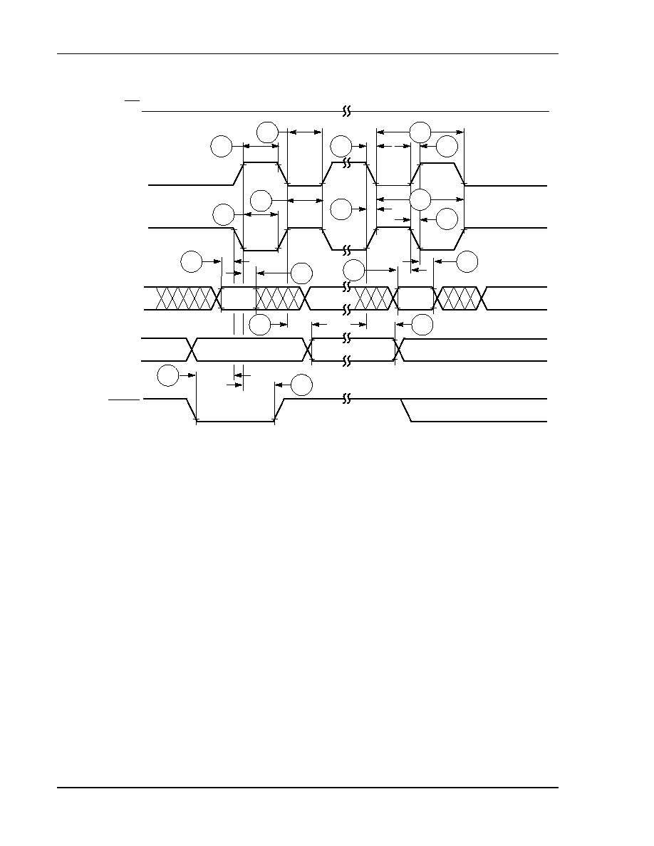
Preliminary Information
2-20
DSP56011 Technical Data Sheet, Rev. 1
MOTOROLA
Specifications
Serial Host Interface (SHI) SPI Protocol Timing
PRELIMINARY
Figure 2-15 SPI Master Timing (CPHA = 0)
SS
(Input)
SCK (CPOL = 0)
(Output)
SCK (CPOL = 1)
(Output)
MISO
(Input)
Valid
MOSI
(Output)
MSB
Valid
LSB
MSB
LSB
HREQ
(Input)
141
142
143
144
144
141
144
144
143
142
148
149
149
148
152
153
163
161
AA0271

Preliminary Information
MOTOROLA
DSP56011 Technical Data Sheet, Rev. 1
2-21
Specifications
Serial Host Interface (SHI) SPI Protocol Timing
PRELIMINARY
Figure 2-16 SPI Master Timing (CPHA = 1)
SS
(Input)
SCK (CPOL = 0)
(Output)
SCK (CPOL = 1)
(Output)
MISO
(Input)
Valid
MOSI
(Output)
MSB
Valid
LSB
MSB
LSB
HREQ
(Input)
141
142
143
144
144
141
144
144
143
142
148
148
149
152
153
163
161
162
149
AA0272
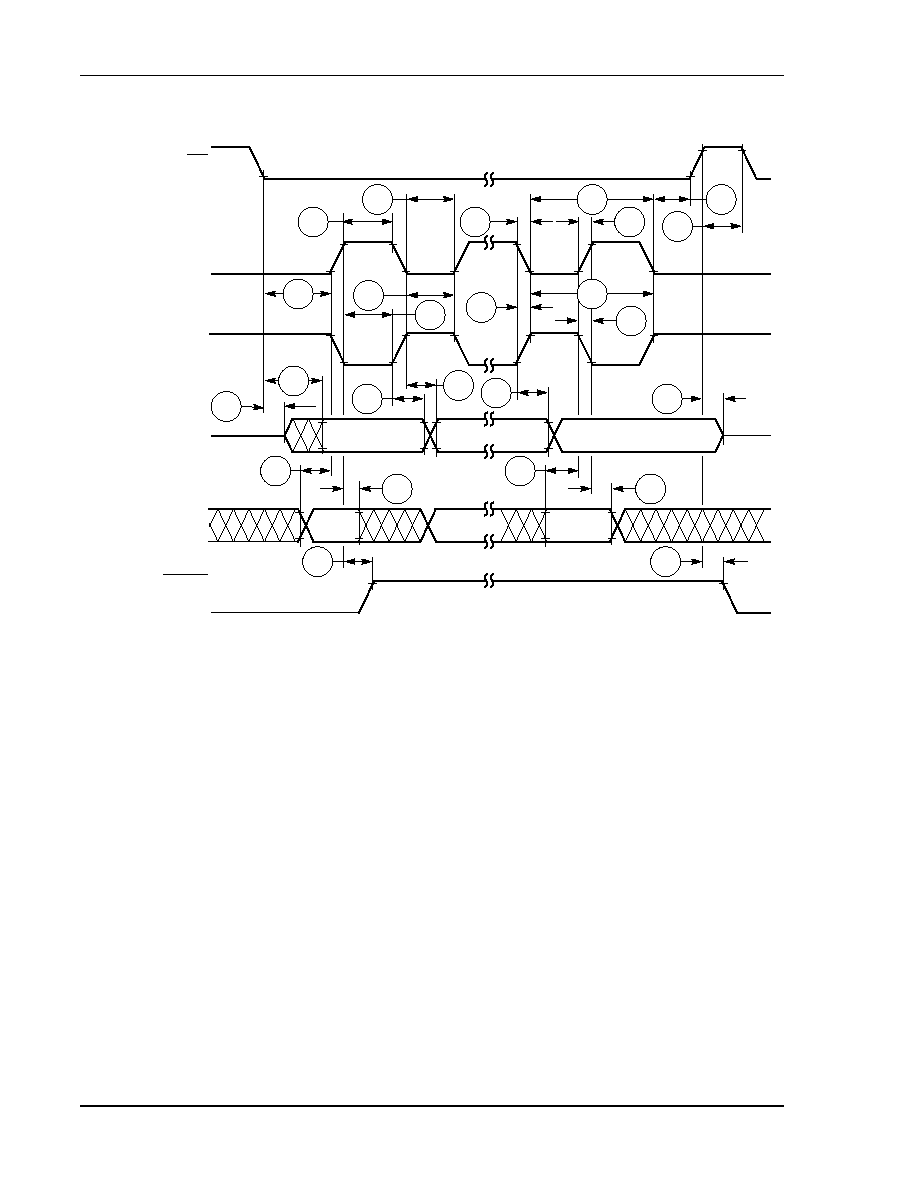
Preliminary Information
2-22
DSP56011 Technical Data Sheet, Rev. 1
MOTOROLA
Specifications
Serial Host Interface (SHI) SPI Protocol Timing
PRELIMINARY
Figure 2-17 SPI Slave Timing (CPHA = 0)
SS
(Input)
SCK (CPOL = 0)
(Input)
SCK (CPOL = 1)
(Input)
MISO
(Output)
MOSI
(Input)
MSB
LSB
MSB
LSB
HREQ
(Output)
141
142
143
144
144
141
144
144
143
142
154
150
152
153
148
149
159
157
153
151
Valid
Valid
148
149
147
160
146
AA0273
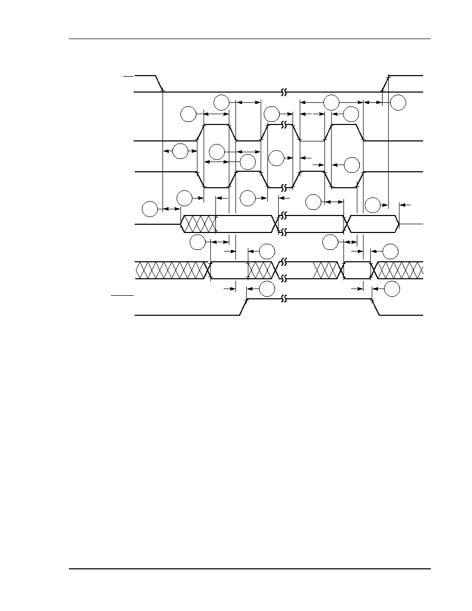
Preliminary Information
MOTOROLA
DSP56011 Technical Data Sheet, Rev. 1
2-23
Specifications
Serial Host Interface (SHI) SPI Protocol Timing
PRELIMINARY
Figure 2-18 SPI Slave Timing (CPHA = 1)
SS
(Input)
SCK (CPOL = 0)
(Input)
SCK (CPOL = 1)
(Input)
MISO
(Output)
MOSI
(Input)
MSB
LSB
MSB
LSB
HREQ
(Output)
141
142
143
144
144
144
144
143
142
150
152
148
149
158
153
151
Valid
Valid
148
147
146
152
149
157
AA0274

Preliminary Information
2-24
DSP56011 Technical Data Sheet, Rev. 1
MOTOROLA
Specifications
Serial Host Interface (SHI) I2C Protocol Timing
PRELIMINARY
SERIAL HOST INTERFACE (SHI) I
2
C PROTOCOL TIMING
R
P
(min) = 1.5 k
Table 2-11
SHI I
2
C Protocol Timing
Standard I
2
C
(C
L
= 400 pF, R
P
= 2 k
, 100 kHz)
No.
Characteristics
Symbol
All Frequencies
Unit
Min
Max
Tolerable spike width on SCL or SDA filters
bypassed
--
0
ns
Narrow filters enabled
--
20
ns
Wide filters enabled
--
100
ns
171
Minimum SCL Serial Clock cycle
T
SCL
10.0
--
�
s
172
Bus free time
T
BUF
4.7
--
�
s
173
Start condition setup time
T
SU;STA
4.7
--
�
s
174
Start condition hold time
T
HD;STA
4.0
--
�
s
175
SCL low period
T
LOW
4.7
--
�
s
176
SCL high period
T
HIGH
4.0
--
�
s
177
SCL and SDA rise time
T
R
--
1.0
�
s
178
SCL and SDA fall time
T
F
--
0.3
�
s
179
Data setup time
T
SU;DAT
250
--
ns
180
Data hold time
T
HD;DAT
0.0
--
ns
182
SCL low to data output valid
T
VD;DAT
--
3.4
�
s
183
Stop condition setup time
T
SU;STO
4.0
--
�
s

Preliminary Information
MOTOROLA
DSP56011 Technical Data Sheet, Rev. 1
2-25
Specifications
Serial Host Interface (SHI) I2C Protocol Timing
PRELIMINARY
Programming the Serial Clock
The Programmed Serial Clock Cycle, t
I
2
CCP
, is specified by the value of the HDM5�
HDM0 and HRS bits of the HCKR (SHI Clock control Register).
The expression for t
I
2
CCP
is:
t
I
2
CCP
= [T
C
�
2
�
(HDM[5:0] + 1)
�
(7
�
(1 � HRS) + 1)]
where
�
HRS is the Prescaler Rate Select bit. When HRS is cleared, the fixed divide-
by-eight prescaler is operational. When HRS is set, the prescaler is
bypassed.
�
MDM5�HDM0 are the Divider Modulus Select bits.
�
A divide ratio from 1 to 64 (HDM5�HDM0 = 0 to $3F) may be selected.
In I
2
C mode, you may select a value for the Programmed Serial Clock Cycle from:
6
�
T
C
(if HDM[5:0] = $02 and HRS = 1)
to
1024
�
T
C
(if HDM[5:0] = $3F and HRS = 0)
The DSP56011 provides an improved I
2
C bus protocol. In addition to supporting the
100 kHz I
2
C bus protocol, the SHI in I
2
C mode supports data transfers at up to 1000
kHz. The actual maximum frequency is limited by the bus capacitances (C
L
),the pull-
up resistors (R
P
), (which affect the rise and fall time of SDA and SCL, see Table 2-12
on page 2-26), and by the input filters.

Preliminary Information
2-26
DSP56011 Technical Data Sheet, Rev. 1
MOTOROLA
Specifications
Serial Host Interface (SHI) I2C Protocol Timing
PRELIMINARY
Considerations for Programming the SHI Clock Control Register
(HCKR)--Clock Divide Ratio
The master must generate a bus free time greater than T172 slave when operating
with a DSP56011 SHI I
2
C slave.
Table 2-12
describes a few examples.
Example:
for C
L
= 50 pF, R
P
= 2 k
, f = 81 MHz, Bypassed filter mode: The master,
when operating with a DSP56011 SHI I
2
C slave with an 81 MHz operating frequency,
must generate a bus free time greater than 36 ns (T172 slave). Thus, the minimum
permissible T
I
2
CCP
is 52
�
T
C
, which gives a bus free time of at least 41 ns (T172
master). This implies a maximum I
2
C serial frequency of 1010 kHz.
In general, bus performance may be calculated from the C
L
and R
P
of the bus,
the input filter modes and operating frequencies of the master and the slave.
Table 2-13
on page 2-27 contains the expressions required to calculate all relevant
performance timing for a given C
L
and R
P
.
Note:
T177 (t
r
) is computed using the values of C
L
and R
P
and T178 (T
F
) is
computed using the value of C
L
. The two values are used in computing many
of the other timing values in Table 2-13 on page 2-27.
Table 2-12
Considerations for Programming the SHI Clock control Register (HCKR)
Conditions to be Considered
Resulting Limitations
Bus Load
Master
Oper-
ating
Freq.
Slave
Oper-
ating
Freq.
Master
Filter
Mode
Slave
Filter
Mode
T172
Slave
Min.
Perm-
issible
t
I
2
CCP
T172
Master
Maximum
I
2
C Serial
Frequency
C
L
= 50 pF,
R
P
= 2 k
81 MHz
81 MHz
Bypassed
Narrow
Wide
Bypassed
Narrow
Wide
36 ns
60 ns
95 ns
52
�
T
C
56
�
T
C
62
�
T
C
41 ns
66 ns
103 ns
1010 kHz
825 kHz
634 kHz
C
L
= 50 pF,
R
P
= 2 k
95 MHz
95 MHz
Bypassed
Narrow
Wide
Bypassed
Narrow
Wide
32 ns
56 ns
91 ns
60
�
T
C
64
�
T
C
71
�
T
C
35 ns
56 ns
92.8 ns
1030 kHz
843 kHz
645 kHz

Preliminary Information
MOTOROLA
DSP56011 Technical Data Sheet, Rev. 1
2-27
Specifications
Serial Host Interface (SHI) I2C Protocol Timing
PRELIMINARY
Table 2-13
SHI Improved I
2
C Protocol Timing
Improved I
2
C (C
L
= 50 pF, R
P
= 2 k
)
No.
Characteristic
Sym.
Mode
Filter
Mode
Expression
81 MHz
2
95 MHz
3
Unit
Min Max Min
Max
-- Tolerable spike
width on SCL or
SDA
Bypassed
Narrow
Wide
0
20
100
--
--
--
0
20
100
--
--
--
0
20
100
ns
ns
ns
171 SCL Serial Clock
cycle
T
SCL
Master Bypassed
T
I
2
CCP
+ 3
�
T
C
+
72 +T
R
989
--
971.5
--
ns
Narrow
T
I
2
CCP
+ 3
�
T
C
+
245 + T
R
1212
--
1186.5
--
ns
Wide
T
I
2
CCP
+ 3
�
T
C
+
535 + T
R
1576
--
1550
--
ns
Slave
Bypassed 4
�
T
C
+ T
H
+ 172 +
T
R
466
--
457.3
--
ns
Narrow
4
�
T
C
+ T
H
+ 366 +
T
R
660
--
651.3
--
ns
Wide
4
�
T
C
+ T
H
+ 648 +
T
R
942
--
933.3
--
ns
172 Bus free time
T
BUF
Master Bypassed 0.5
�
T
I
2
CCP
� 42 � T
R
41.1
--
35
--
ns
Narrow
0.5
�
T
I
2
CCP
� 42 � T
R
65.8
--
56
--
ns
Wide
0.5
�
T
I
2
CCP
� 42 � T
R
103
--
92.8
--
ns
Slave
Bypassed
2
�
T
C
+ 11
35.7
--
32
--
ns
Narrow
2
�
T
C
+ 35
59.7
--
56
--
ns
Wide
2
�
T
C
+ 70
94.7
--
91
--
ns
173 Start condition
setup time
T
SU;STA
Slave
Bypassed
12
12
--
12
--
ns
Narrow
50
50
--
50
--
ns
Wide
150
150
--
150
--
ns
174 Start condition
hold time
T
HD;STA
Master Bypassed 0.5
�
T
I
2
CCP
+ 12 � T
F
313
--
307
--
ns
Narrow 0.5
�
T
I
2
CCP
+ 12 � T
F
338
--
328
--
ns
Wide
0.5
�
T
I
2
CCP
+ 12 � T
F
375
--
364.8
--
ns
Slave
Bypassed
2
�
T
C
+ T
H
+ 21
51.9
--
47.25
--
ns
Narrow
2
�
T
C
+ T
H
+ 100
131
--
126.25
--
ns
Wide
2
�
T
C
+ T
H
+ 200
231
--
226.25
--
ns

Preliminary Information
2-28
DSP56011 Technical Data Sheet, Rev. 1
MOTOROLA
Specifications
Serial Host Interface (SHI) I2C Protocol Timing
PRELIMINARY
175 SCL low period
T
LOW
Master Bypassed 0.5
�
T
I
2
CCP
+ 18 � T
F
319
--
313
--
ns
Narrow
0.5
�
T
I
2
CCP
+ 18 � T
F
344
--
334
--
ns
Wide
0.5
�
T
I
2
CCP
+ 18 � T
F
381
--
370.75
--
ns
Slave
Bypassed
2
�
T
C
+ 74 + T
R
337
--
333
--
ns
Narrow
2
�
T
C
+ 286 + T
R
548.6 --
545
--
ns
Wide
2
�
T
C
+ 586 + T
R
849
--
845
--
ns
176 SCL high period
T
HIGH
Master Bypassed 0.5
�
T
I
2
CCP
+2
�
T
C
+ 19
365
--
355
--
ns
Narrow
0.5
�
T
I
2
CCP
+2
�
T
C
+ 144
514
--
501
--
ns
Wide
0.5
�
T
I
2
CCP
+ 2
�
T
C
+ 356
763
--
749.8
--
ns
Slave
Bypassed
2
�
T
C
+ T
H
� 1
30
--
25.25
--
ns
Narrow
2
�
T
C
+ T
H
+ 18
49
--
44.25
--
ns
Wide
2
�
T
C
+ T
H
+ 30
61
--
56.25
--
ns
177 SCL rise time
Output
T
R
1.7
�
R
P
�
(C
L
+ 20)
1
--
238
--
238
ns
Input
2000
--
2000
--
2000
ns
178 SCL fall time
Output
T
F
20 + 0.1
�
(C
L
� 50)
1
--
20
--
20
ns
Input
2000
--
2000
--
2000
ns
179 Data setup time
T
SU;DAT
Bypassed
T
C
+ 8
20
--
18.5
--
ns
Narrow
T
C
+ 60
72
--
70.5
--
ns
Wide
T
C
+ 74
86
--
84.5
--
ns
180 Data hold time
T
HD;DAT
Bypassed
Narrow
Wide
0
0
0
0
0
0
--
--
--
0
0
0
--
--
--
ns
ns
ns
Table 2-13
SHI Improved I
2
C Protocol Timing (Continued)
Improved I
2
C (C
L
= 50 pF, R
P
= 2 k
)
No.
Characteristic
Sym.
Mode
Filter
Mode
Expression
81 MHz
2
95 MHz
3
Unit
Min Max Min
Max
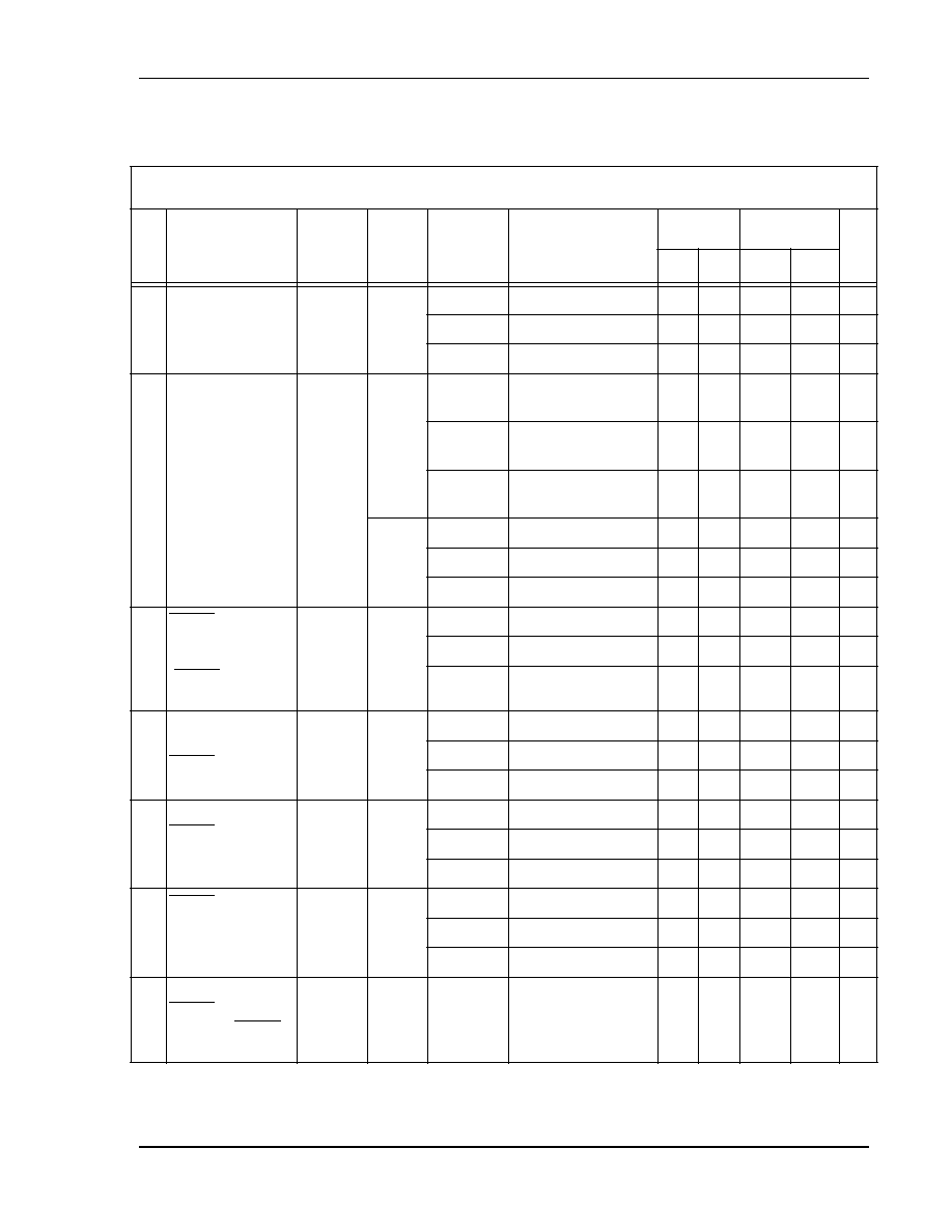
Preliminary Information
MOTOROLA
DSP56011 Technical Data Sheet, Rev. 1
2-29
Specifications
Serial Host Interface (SHI) I2C Protocol Timing
PRELIMINARY
182 SCL low to data
output valid
T
VD;DAT
Bypassed
2
�
T
C
+ 71 + T
R
--
334
--
330
ns
Narrow
2
�
T
C
+ 244 + T
R
--
507
--
503
ns
Wide
2
�
T
C
+ 535 + T
R
--
798
--
794
ns
183 Stop condition
setup time
T
SU;STO
Master Bypassed
0.5
�
T
I
2
CCP
+ T
C
+
T
H
+ 11
351
--
341.75
--
ns
Narrow
0.5
�
T
I
2
CCP
+ T
C
+
T
H
+ 69
433
--
420.75
--
ns
Wide
0.5
�
T
I
2
CCP
+ T
C
+
T
H
+ 183
584
--
571.5
--
ns
Slave
Bypassed
11
11
--
11
--
ns
Narrow
50
50
--
50
--
ns
Wide
150
150
--
150
--
ns
184 HREQ input
deassertion to
last SCL edge
(HREQ in setup
time)
Master Bypassed
0
0
--
0
--
ns
Narrow
0
0
--
0
--
ns
Wide
0
0
--
0
--
ns
186 First SCL
sampling edge to
HREQ output
deassertation
Slave
Bypassed
3
�
T
C
+ T
H
+ 32
--
75
--
68.75
ns
Narrow
3
�
T
C
+ T
H
+ 209
--
252
--
245.75 ns
Wide
3
�
T
C
+ T
H
+ 507
--
550
--
543.7
ns
187 Last SCL edge to
HREQ output not
deasserted
Slave
Bypassed
2
�
T
C
+ T
H
+ 6
37
--
32.25
--
ns
Narrow
2
�
T
C
+ T
H
+ 63
93.9
--
89.25
--
ns
Wide
2
�
T
C
+ T
H
+ 169
200
--
195.25
--
ns
188 HREQ input
assertion to first
SCL edge
Master Bypassed
T
I
2
CCP
+ 2
�
T
C
+ 6
673
--
657
--
ns
Narrow
T
I
2
CCP
+ 2
�
T
C
+ 6
722
--
699
--
ns
Wide
T
I
2
CCP
+ 2
�
T
C
+ 6
796
--
772.5
--
ns
189 First SCL edge to
HREQ input not
asserted (HREQ
input hold time)
Master
0
0
--
0
--
ns
Table 2-13
SHI Improved I
2
C Protocol Timing (Continued)
Improved I
2
C (C
L
= 50 pF, R
P
= 2 k
)
No.
Characteristic
Sym.
Mode
Filter
Mode
Expression
81 MHz
2
95 MHz
3
Unit
Min Max Min
Max

Preliminary Information
2-30
DSP56011 Technical Data Sheet, Rev. 1
MOTOROLA
Specifications
Serial Host Interface (SHI) I2C Protocol Timing
PRELIMINARY
Notes:
1.
C
L
is in pF, R
P
is in k
, and result is in ns.
2.
A T
I
2
CCP
of 52
�
T
C
(the maximum permitted for the given bus load) was used for the calculations in the
Bypassed filter mode. A T
I
2
CCP
of 56
�
T
C
(the maximum permitted for the given bus load) was used for the
calculations in the Narrow filter mode. A T
I
2
CCP
of 62
�
T
C
(the maximum permitted for the given bus
load) was used for the calculations in the Wide filter mode.
3.
A T
I
2
CCP
of 60
�
T
C
(the maximum permitted for the given bus load) was used for the calculations in the
Bypassed filter mode. A T
I
2
CCP
of 64
�
T
C
(the maximum permitted for the given bus load) was used for the
calculations in the Narrow filter mode. A T
I
2
CCP
of 71
�
T
C
(the maximum permitted for the given bus
load) was used for the calculations in the Wide filter mode.
Figure 2-19 I
2
C Timing
Table 2-13
SHI Improved I
2
C Protocol Timing (Continued)
Improved I
2
C (C
L
= 50 pF, R
P
= 2 k
)
No.
Characteristic
Sym.
Mode
Filter
Mode
Expression
81 MHz
2
95 MHz
3
Unit
Min Max Min
Max
Start
SCL
HREQ
SDA
ACK
MSB
LSB
Stop
171
Stop
173
176
175
177
178
180
179
172
186
182
183
189
174
188
184
187
AA0275

Preliminary Information
MOTOROLA
DSP56011 Technical Data Sheet, Rev. 1
2-31
Specifications
General Purpose Input/Output (GPIO) Timing
PRELIMINARY
GENERAL PURPOSE INPUT/OUTPUT (GPIO) TIMING
Table 2-14
GPIO Timing
No.
Characteristics
Expression
All Frequencies
Unit
Min
Max
201
EXTAL edge to GPIO output valid (GPIO output
delay time)
26
--
26
ns
202
EXTAL edge to GPIO output not valid (GPIO
output hold time)
2
2
--
ns
203
GPIO input valid to EXTAL Edge (GPIO input
setup time)
10
10
--
ns
204
EXTAL edge to GPIO input not valid (GPIO input
hold time)
6
6
--
ns
Figure 2-20 GPIO Timing
Valid
(Input)
(Output)
EXTAL
(Input)
(see Note)
Note:
Valid when the ratio between EXTAL frequency and internal clock frequency equals 1
201
202
204
203
PB0�PB14
PB0�PB14
GPIO0�GPIO7
GPIO0�GPIO7
AA1284

Preliminary Information
2-32
DSP56011 Technical Data Sheet, Rev. 1
MOTOROLA
Specifications
Digital Audio Transmitter (DAX) Timing
PRELIMINARY
DIGITAL AUDIO TRANSMITTER (DAX) TIMING
Table 2-15
56011 Digital Audio Transmitter Timing
No.
Characteristic
All Frequencies
Unit
Min
Max
ACI Frequency (see Note)
--
25
MHz
220
ACI Period
40
--
ns
221
ACI High Duration
0.5
�
T
C
--
ns
222
ACI Low Duration
0.5
�
T
C
--
ns
223
ACI Rising Edge to ADO Valid
--
35
ns
Note:
In order to assure proper operation of the DAX, the ACI frequency should be less than 1/2 of the
DSP56011 internal clock frequency. For example, if the DSP56011 is running at 40 MHz internally,
the ACI frequency should be less than 20 MHz.
Figure 2-21 Digital Audio Transmitter Timing
ACI
ADO
220
223
AA1280
221
222
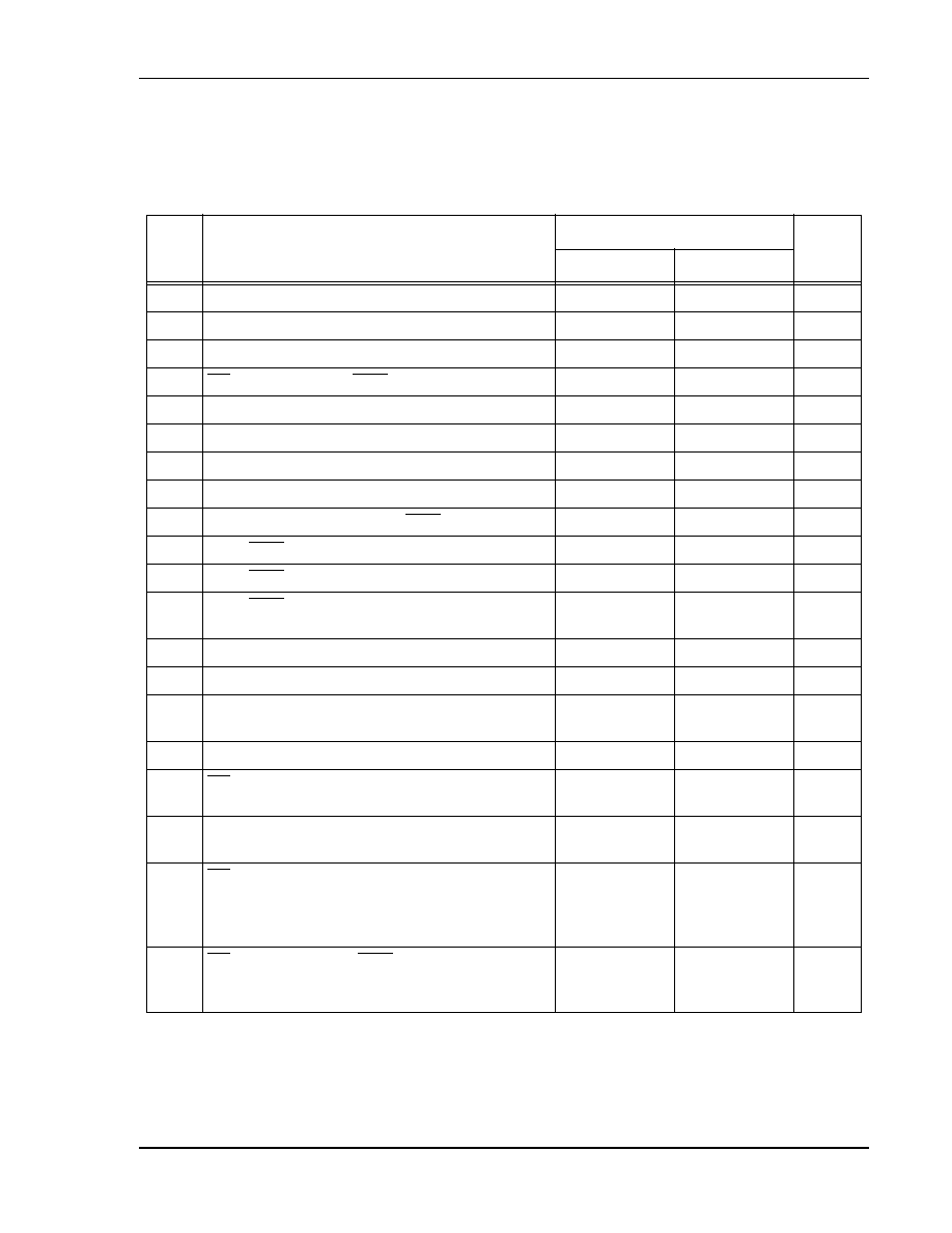
Preliminary Information
MOTOROLA
DSP56011 Technical Data Sheet, Rev. 1
2-33
Specifications
On-Chip Emulation (OnCE
TM
) Timing
PRELIMINARY
ON-CHIP EMULATION (OnCE
TM
) TIMING
Table 2-16
OnCE Timing
No.
Characteristics
All Frequencies
Unit
Min Max
230
DSCK low
40
--
ns
231
DSCK high
40
--
ns
232
DSCK cycle time
200
--
ns
233
DR asserted to DSO (ACK) asserted
5 T
C
--
ns
234
DSCK high to DSO valid
--
42
ns
235
DSCK high to DSO invalid
3
--
ns
236
DSI valid to DSCK low (setup)
15
--
ns
237
DSCK Low to DSI Invalid (Hold)
3
--
ns
238
Last DSCK low to OS0�OS1, ACK active
3 T
C
+ T
L
--
ns
239
DSO (ACK) asserted to first DSCK high
2 T
C
--
ns
240
DSO (ACK) assertion width
4 T
C
+ T
H
� 3
5 T
C
+ 7
ns
241
DSO (ACK) asserted to OS0�OS1 high
impedance
1
--
0
ns
242
OS0�OS1 valid to second EXTAL transition
T
C
� 21
--
ns
243
Second EXTAL transition to OS0�OS1 invalid
0
--
ns
244
Last DSCK low of read register to first DSCK high
of next command
7 T
C
+ 10
--
ns
245
Last DSCK low to DSO invalid (hold)
3
--
ns
246
DR assertion to second EXTAL transition for
wake up from Wait state
10
T
C
� 10
ns
247
Second EXTAL transition to DSO after wake up
from Wait state
17 T
C
--
ns
248
DR assertion width
�
To recover from Wait
�
To recover from Wait and enter Debug
mode
15
13 T
C
+ 15
12 T
C
� 15
--
ns
249
DR assertion to DSO (ACK) valid (enter Debug
mode) after asynchronous recovery from Wait
state
17 T
C
--
ns
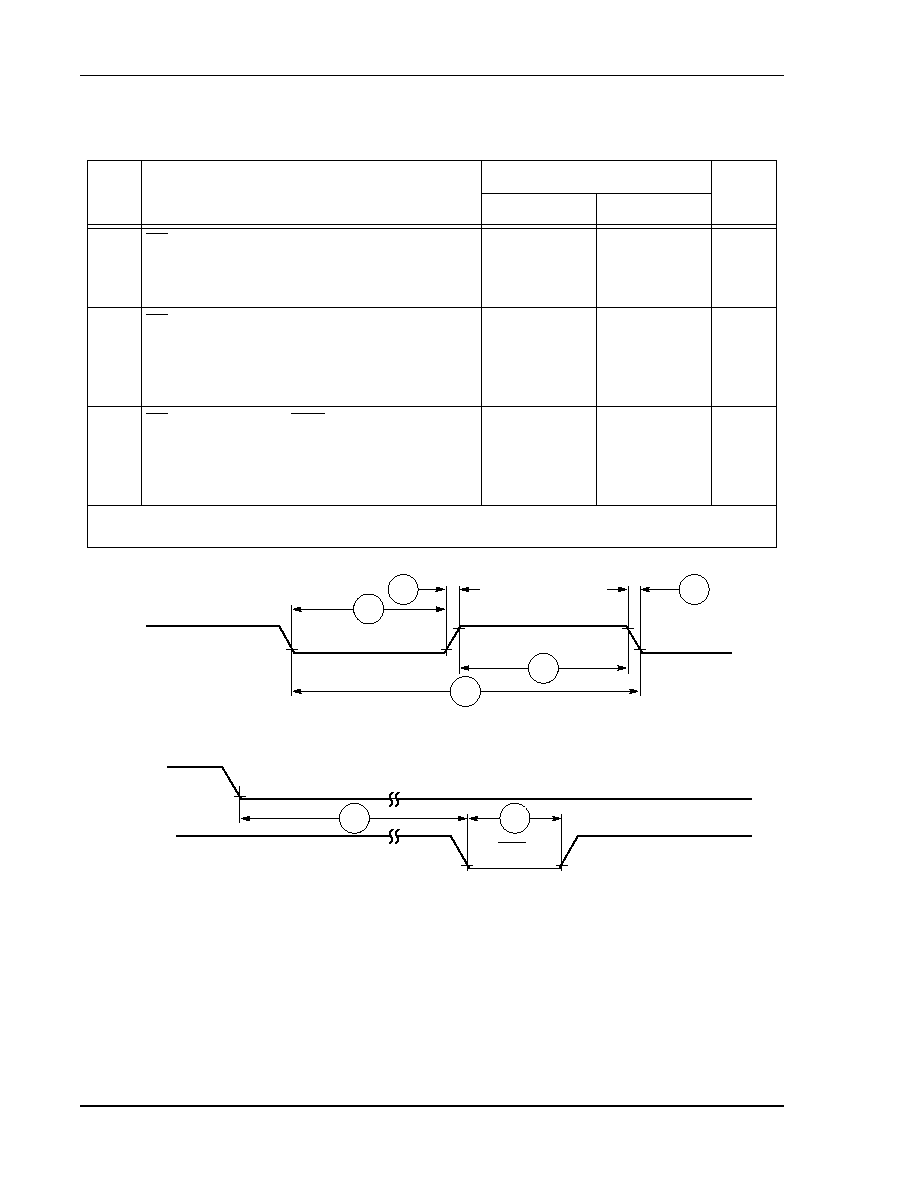
Preliminary Information
2-34
DSP56011 Technical Data Sheet, Rev. 1
MOTOROLA
Specifications
On-Chip Emulation (OnCE
TM
) Timing
PRELIMINARY
250A DR assertion width to recover from Stop
2
�
Stable External Clock, OMR Bit 6 = 0
�
Stable External Clock, OMR Bit 6 = 1
�
Stable External Clock, PCTL Bit 17 = 1
15
15
15
65548 T
C
+ T
L
20 T
C
+ T
L
13 T
C
+ T
L
ns
250B
DR assertion width to recover from Stop and enter
Debug mode
2
�
Stable External Clock, OMR Bit 6 = 0
�
Stable External Clock, OMR Bit 6 = 1
�
Stable External Clock, PCTL Bit 17= 1
65549 T
C
+ T
L
21 T
C
+ T
L
14 T
C
+ T
L
--
--
--
ns
251
DR assertion to DSO (ACK) valid (enter Debug
mode) after recovery from Stop state
2
�
Stable External Clock, OMR Bit 6 = 0
�
Stable External Clock, OMR Bit 6 = 1
�
Stable External Clock, PCTL Bit 17= 1
65553 T
C
+ T
L
25 T
C
+ T
L
18 T
C
+ T
L
--
--
--
ns
Notes:
1.
Maximum T
L
2.
Periodically sampled, not 100% tested
Figure 2-22 DSP56011 OnCE Serial Clock Timing
Figure 2-23 DSP56011 OnCE Acknowledge Timing
Table 2-16
OnCE Timing (Continued)
No.
Characteristics
All Frequencies
Unit
Min Max
DSCK
(input)
246
246
231
232
230
AA0277
DR
(Input)
DSO
(Output)
ACK
233
240
AA0278
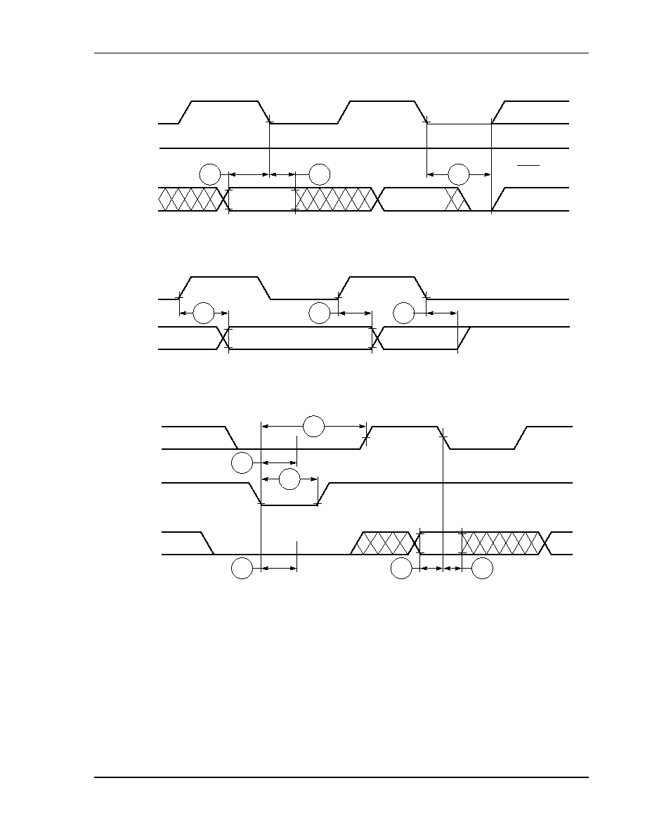
Preliminary Information
MOTOROLA
DSP56011 Technical Data Sheet, Rev. 1
2-35
Specifications
On-Chip Emulation (OnCE
TM
) Timing
PRELIMINARY
Figure 2-24 DSP56011 OnCE Data I/O to Status Timing
Figure 2-25 DSP56011 OnCE Read Timing
Figure 2-26 DSP56011 OnCE Data I/O Status Timing
DSCK
(Input)
DSO
(Output)
(ACK)
(OS1)
DSI
(Input)
(OS0)
(Note 1)
Note:
High Impedance, external pull-down resistor
(Last)
236
237
238
AA0279
DSCK
(Input)
DSO
(Output)
(OS0)
(Note 1)
Note:
High Impedance, external pull-down resistor
(Last)
235
245
234
AA0280
Note:
High Impedance, external pull-down resistor
OS1
(Output)
DSO
(Output)
(DSCK Input)
OS0
(Output)
(see Note)
(DSO Output)
(DSI Input)
(see Note)
241
239
240
241
236
237
AA1281
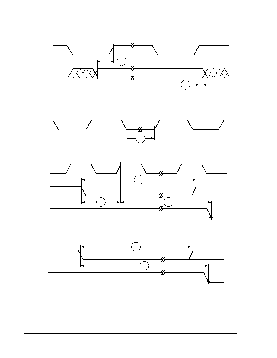
Preliminary Information
2-36
DSP56011 Technical Data Sheet, Rev. 1
MOTOROLA
Specifications
On-Chip Emulation (OnCE
TM
) Timing
PRELIMINARY
Figure 2-27 DSP56011 OnCE EXTAL to Status Timing
Figure 2-28 DSP56011 OnCE DSCK Next Command After Read Register Timing
Figure 2-29 Synchronous Recovery from Wait State
Figure 2-30 Asynchronous Recovery from Wait State
EXTAL
OS0�OS1
(Output)
Note:
1.
High Impedance, external pull-down resistor
2.
Valid when the ratio between EXTAL frequency and clock frequency equals 1
(Note 1)
(Note 2)
242
243
AA0282
DSCK
(Input)
(Next Command)
244
AA0283
T0, T2
T1, T3
EXTAL
DR
(Input)
DSO
(Output)
248
246
247
AA0284
DR
(Input)
DSO
(Output)
248
249
AA0285

Preliminary Information
MOTOROLA
DSP56011 Technical Data Sheet, Rev. 1
2-37
Specifications
On-Chip Emulation (OnCE
TM
) Timing
PRELIMINARY
Figure 2-31 Asynchronous Recovery from Stop State
DR
(Input)
DSO
(Output)
250
251
AA0286

Preliminary Information
2-38
DSP56011 Technical Data Sheet, Rev. 1
MOTOROLA
Specifications
On-Chip Emulation (OnCE
TM
) Timing
PRELIMINARY

Preliminary Information
MOTOROLA
DSP56011 Technical Data Sheet, Rev. 1
3-1
PRELIMINARY
SECTION
3
PACKAGING
PIN-OUT AND PACKAGE INFORMATION
This sections provides information about the available packages for this product,
including diagrams of the package pinouts and tables describing how the signals
described in
Section 1
are allocated. The DSP56011 is available in a 100-pin Thin
Quad Flat Pack (TQFP) package.
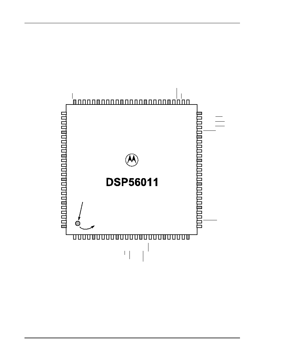
Preliminary Information
3-2
DSP56011 Technical Data Sheet, Rev. 1
MOTOROLA
Packaging
Pin-out and Package Information
PRELIMINARY
TQFP Package Description
Top and bottom views of the TQFP package are shown in
Figure 3-1
and
Figure 3-2
with their pin-outs.
Figure 3-1 DSP56011 Thin Quad Flat Pack (TQFP), Top View
Orientation Mark
1
26
(Top View)
25
50
75
51
76
100
GPIO7
GPIO6
GND
D
GPIO5
GPIO4
V
CCD
GPIO3
GPIO2
GND
D
GPIO1
GPIO0
GND
Q
V
CCQ
not connected
not connected
GND
A
not connected
V
CCA
not connected
not connected
GND
A
not connected
not connected
not connected
V
CCA
DR
not connected
not connected
not connected
not connected
DSCK/OS1
DSI/OS0
DSO
SDI0
SDI1
WSR
GND
S
V
CCQ
GND
Q
SCKR
WST
SCKT
V
CCS
SDO0
SDO1
SDO2
GND
S
HREQ
SS
/HA2
MOSI/HA0
not connected
not connected
GND
A
not connected
not connected
H7/PB7
H6/PB6
GND
H
HOA2/PB10
V
CCH
HOA1/PB9
HR/W
/PB11
HEN
/PB12
V
CCQ
GND
Q
HACK
/PB14
GND
H
HOA0/PB8
H5/PB5
V
CCH
H4/PB4
H3/PB3
GND
H
H2/PB2
H1/PB1
V
CCS
MODC/NMI
MODB/IRQB
MODA/IRQA
RESET
MISO/SDA
GND
S
SCK/SCL
EXTAL
V
CCP
PCAP
GND
P
PINIT
GND
Q
V
CCQ
PLOCK
not connected
not connected
not connected
ACI
ADO
V
CCH
GND
H
HOREQ/PB13
H0/PB0
AA1282

Preliminary Information
MOTOROLA
DSP56011 Technical Data Sheet, Rev. 1
3-3
Packaging
Pin-out and Package Information
PRELIMINARY
Figure 3-2 DSP56011 Thin Quad Flat Pack (TQFP), Bottom View
Orientation Mark
1
26
(Bottom View)
25
50
75
51
76
100
GPIO7
GPIO6
GND
D
GPIO5
GPIO4
V
CCD
GPIO3
GPIO2
GND
D
GPIO1
GPIO0
GND
Q
V
CCQ
not connected
not connected
GND
A
not connected
V
CCA
not connected
not connected
GND
A
not connected
not connected
not connected
V
CCA
V
CCS
MODC/NMI
MODB/IRQB
MODA/IRQA
RESET
MISO/SDA
GND
S
SCK/SCL
EXTAL
V
CCP
PCAP
GND
P
PINIT
GND
Q
V
CCQ
PLOCK
not connected
not connected
not connected
ACI
ADO
V
CCH
GND
H
HOREQ/PB13
H0/PB0
DR
not connected
not connected
not connected
not connected
DSCK/OS1
DSI/OS0
DSO
SDI0
SDI1
WSR
GND
S
V
CCQ
GND
Q
SCKR
WST
SCKT
V
CCS
SDO0
SDO1
SDO2
GND
S
HREQ
SS
/HA2
MOSI
/HA0
not connected
not connected
GND
A
not connected
not connected
H7/PB7
H6/PB6
GND
H
HOA2/PB10
V
CCH
HOA1/PB9
HR/W
/PB11
HEN
/PB12
V
CCQ
GND
Q
HACK
/PB14
GND
H
HOA0/PB8
H5/PB5
V
CCH
H4/PB4
H3/PB3
GND
H
H2/PB2
H1/PB1
AA1283

Preliminary Information
3-4
DSP56011 Technical Data Sheet, Rev. 1
MOTOROLA
Packaging
Pin-out and Package Information
PRELIMINARY
Table 3-1
Signal by Pin Number
Pin #
Signal Name
Pin
#
Signal Name
Pin #
Signal Name
Pin
#
Signal Name
1
not connected
26
H0/PB0
51
MOSI/HA0
76
GPIO7
2
not connected
27
HOREQ/
PB13
52
SS/HA2
77
GPIO6
3
GND
A
28
GND
H
53
HREQ
78
GND
D
4
not connected
29
V
CCH
54
GND
S
79
GPIO5
5
not connected
30
ADO
55
SDO2
80
GPIO4
6
H7/PB7
31
ACI
56
SDO1
81
V
CCD
7
H6/PB6
32
not connected
57
SDO0
82
GPIO3
8
GND
H
33
not connected
58
V
CCS
83
GPIO2
9
HOA2/PB10
34
not connected
59
SCKT
84
GND
D
10
V
CCH
35
PLOCK
60
WST
85
GPIO1
11
HOA1/PB9
36
V
CCQ
61
SCKR
86
GPIO0
12
HR/W/PB11
37
GND
Q
62
GND
Q
87
GND
Q
13
HEN/PB12
38
PINIT
63
V
CCQ
88
V
CCQ
14
V
CCQ
39
GND
P
64
GND
S
89
not connected
15
GND
Q
40
PCAP
65
WSR
90
not connected
16
HACK/PB14
41
V
CCP
66
SDI1
91
GND
A
17
GND
H
42
EXTAL
67
SDI0
92
not connected
18
HOA0/PB8
43
SCK/SCL
68
DSO
93
V
CCA
19
H5/PB5
44
GND
S
69
DSI/OS0
94
not connected
20
V
CCH
45
MISO/SDA
70
DSCK/OS1
95
not connected
21
H4/PB4
46
RESET
71
not connected
96
GND
A
22
H3/PB3
47
MODA/
IRQA
72
not connected
97
not connected
23
GND
H
48
MODB/IRQB
73
not connected
98
not connected
24
H2/PB2
49
MODC/NMI
74
not connected
99
not connected
25
H1/PB1
50
V
CCS
75
DR
100
V
CCA

Preliminary Information
MOTOROLA
DSP56011 Technical Data Sheet, Rev. 1
3-5
Packaging
Pin-out and Package Information
PRELIMINARY
Table 3-2
Signal by Name
Signal Name
Pin
#
Signal Name
Pin #
Signal Name
Pin
#
Signal Name
Pin #
ACI
31
GPIO7
76
not connected
32
PB14
16
ADO
30
H0
26
not connected
33
PCAP
40
DR
75
H1
25
not connected
34
PINIT
38
DSCK
70
H2
24
not connected
71
PLOCK
35
DSI
69
H3
22
not connected
72
RESET
46
DSO
68
H4
21
not connected
73
SCK
43
EXTAL
42
H5
19
not connected
74
SCKR
61
GND
A
3
H6
7
not connected
89
SCKT
59
GND
A
91
H7
6
not connected
90
SCL
43
GND
A
96
HA0
51
not connected
92
SDA
45
GND
D
78
HA2
52
not connected
94
SDI0
67
GND
D
84
HACK
16
not connected
95
SDI1
66
GND
H
8
HEN
13
not connected
97
SDO0
57
GND
H
17
HOA0
18
not connected
98
SDO1
56
GND
H
23
HOA1
11
not connected
99
SDO2
55
GND
H
28
HOA2
9
OS0
69
SS
52
GND
P
39
HOREQ
27
OS1
70
V
CCA
93
GND
Q
15
HREQ
53
PB0
26
V
CCA
100
GND
Q
37
HR/W
12
PB1
25
V
CCD
81
GND
Q
62
IRQA
47
PB2
24
V
CCH
10
GND
Q
87
IRQB
48
PB3
22
V
CCH
20
GND
S
44
MISO
45
PB4
21
V
CCH
29
GND
S
64
MODA
47
PB5
19
V
CCP
41
GND
S
54
MODB
48
PB6
7
V
CCQ
14
GPIO0
86
MODC
49
PB7
6
V
CCQ
36
GPIO1
85
MOSI
51
PB8
18
V
CCQ
63
GPIO2
83
NMI
49
PB9
11
V
CCQ
88
GPIO3
82
not connected
1
PB10
9
V
CCS
50
GPIO4
80
not connected
2
PB11
12
V
CCS
58
GPIO5
79
not connected
4
PB12
13
WSR
65
GPIO6
77
not connected
5
PB13
27
WST
60

Preliminary Information
3-6
DSP56011 Technical Data Sheet, Rev. 1
MOTOROLA
Packaging
Pin-out and Package Information
PRELIMINARY
Figure 3-3 100-pin Thin Quad Flat Pack (TQFP) Mechanical Information
DIM
A
MIN
MAX
14.00 BSC
MILLIMETERS
A1
7.00 BSC
B
14.00 BSC
B1
7.00 BSC
C
1.70
C1
0.05
0.20
C2
1.30
1.50
D
0.10
0.30
E
0.45
0.75
F
0.15
0.23
G
0.50 BSC
J
0.07
0.20
K
0.50 REF
R1
0.08
0.20
S
16.00 BSC
S1
8.00 BSC
U
0.09
0.16
V
16.00 BSC
V1
8.00 BSC
W
0.20 REF
Z
1.00 REF
NOTES:
1.
DIMENSIONS AND TOLERANCES PER ASME Y14.5M,
1994.
2.
DIMENSIONS IN MILLIMETERS.
3.
DATUMS L, M AND N TO BE DETERMINED AT THE
SEATING PLANE, DATUM T.
4.
DIMENSIONS S AND V TO BE DETERMINED AT
SEATING PLANE, DATUM T.
5.
DIMENSIONS A AND B DO NOT INCLUDE MOLD
PROTRUSION. ALLOWABLE PROTRUSION IS 0.25
PER SIDE. DIMENSIONS A AND B INCLUDE MOLD
MISMATCH.
6.
DIMENSION D DOES NOT INCLUDE DAMBAR
PROTRUSION. DAMBAR PROTRUSION SHALL NOT
CAUSE THE LEAD WIDTH TO EXCEED 0.35. MINIMUM
SPACE BETWEEN PROTRUSION AND ADJACENT
LEAD OR PROTRUSION 0.07.
1
2
3
---
--
0�
7�
0�
PLATING
U
J
D
F
ROTATED 90 CLOCKWISE
SECTION AB-AB
BASE METAL
L-M
M
0.08
N
T
C2
C1
(K)
(Z)
(W)
GAGE PLANE
VIEW AA
0.05
E
0.25
1
2X
R R1
VIEW Y
4X 25 TIPS
4X
25
100
76
75
51
26
50
1
N
0.2 T L-M
3X
A
S
A1
S1
B1
V1
B V
N
0.2 T L-M
M
N
L
VIEW AA
C
0.08 T
3
4X
T
SEATING
PLANE
2
4X
100X
VIEW Y
AB
CL
X = L, M, OR N
G
X
AB
CASE 983-02
ISSUE E
12�
REF
12�
REF

Preliminary Information
MOTOROLA
DSP56011 Technical Data Sheet, Rev. 1
3-7
Packaging
Ordering Drawings
PRELIMINARY
ORDERING DRAWINGS
Complete mechanical information regarding DSP56011 packaging is available by
facsimile through Motorola's MfaxTM system. Call the following number to obtain
information by facsimile:
The Mfax automated system requests the following information:
�
The receiving facsimile telephone number including area code or country
code
�
The caller's Personal Identification Number (PIN)
Note:
For first time callers, the system provides instructions for setting up a PIN,
which requires entry of a name and telephone number.
�
The type of information requested:
�
Instructions for using the system
�
A literature order form
�
Specific part technical information or data sheets
�
Other information described by the system messages
A total of three documents may be ordered per call.
The DSP56011 100-pin TQFP package mechanical drawing is referenced as 983-02.
(602) 244-6609

Preliminary Information
3-8
DSP56011 Technical Data Sheet, Rev. 1
MOTOROLA
Packaging
Ordering Drawings
PRELIMINARY

Preliminary Information
MOTOROLA
DSP56011 Technical Data Sheet, Rev. 1
4-1
PRELIMINARY
SECTION
4
DESIGN CONSIDERATIONS
THERMAL DESIGN CONSIDERATIONS
An estimation of the chip junction temperature, T
J
, in
�
C can be obtained from the
equation:
Equation 1:
Where:
T
A
= ambient temperature �C
R
JA
= package junction-to-ambient thermal resistance �C/W
P
D
= power dissipation in package
Historically, thermal resistance has been expressed as the sum of a junction-to-case
thermal resistance and a case-to-ambient thermal resistance:
Equation 2:
Where:
R
JA
= package junction-to-ambient thermal resistance �C/W
R
JC
= package junction-to-case thermal resistance �C/W
R
CA
= package case-to-ambient thermal resistance �C/W
R
JC
is device-related and cannot be influenced by the user. The user controls the
thermal environment to change the case-to-ambient thermal resistance, R
CA
. For
example, the user can change the air flow around the device, add a heat sink, change
the mounting arrangement on the printed circuit board, or otherwise change the
thermal dissipation capability of the area surrounding the device on a printed circuit
board. This model is most useful for ceramic packages with heat sinks; some 90% of
the heat flow is dissipated through the case to the heat sink and out to the ambient
environment. For ceramic packages, in situations where the heat flow is split between
a path to the case and an alternate path through the printed circuit board, analysis of
the device thermal performance may need the additional modeling capability of a
system level thermal simulation tool.
T
J
T
A
P
D
R
JA
�
(
)
+
=
R
JA
R
JC
R
CA
+
=

Preliminary Information
4-2
DSP56011 Technical Data Sheet, Rev. 1
MOTOROLA
Design Considerations
Thermal Design Considerations
PRELIMINARY
The thermal performance of plastic packages is more dependent on the temperature
of the printed circuit board to which the package is mounted. Again, if the
estimations obtained from R
JA
do not satisfactorily answer whether the thermal
performance is adequate, a system level model may be appropriate.
A complicating factor is the existence of three common ways for determining the
junction-to-case thermal resistance in plastic packages:
�
To minimize temperature variation across the surface, the thermal resistance
is measured from the junction to the outside surface of the package (case)
closest to the chip mounting area when that surface has a proper heat sink.
�
To define a value approximately equal to a junction-to-board thermal
resistance, the thermal resistance is measured from the junction to where the
leads are attached to the case.
�
If the temperature of the package case (T
T
) is determined by a thermocouple,
the thermal resistance is computed using the value obtained by the equation
(T
J
� T
T
)/P
D
.
As noted above, the junction-to-case thermal resistances quoted in this data sheet are
determined using the first definition. From a practical standpoint, that value is also
suitable for determining the junction temperature from a case thermocouple reading
in forced convection environments. In natural convection, using the junction-to-case
thermal resistance to estimate junction temperature from a thermocouple reading on
the case of the package will estimate a junction temperature slightly hotter than
actual temperature. Hence, the new thermal metric, Thermal Characterization
Parameter or
JT
, has been defined to be (T
J
� T
T
)/P
D
. This value gives a better
estimate of the junction temperature in natural convection when using the surface
temperature of the package. Remember that surface temperature readings of
packages are subject to significant errors caused by inadequate attachment of the
sensor to the surface and to errors caused by heat loss to the sensor. The
recommended technique is to attach a 40-gauge thermocouple wire and bead to the
top center of the package with thermally conductive epoxy.

Preliminary Information
MOTOROLA
DSP56011 Technical Data Sheet, Rev. 1
4-3
Design Considerations
Electrical Design Considerations
PRELIMINARY
ELECTRICAL DESIGN CONSIDERATIONS
Use the following list of recommendations to assure correct DSP operation:
�
Provide a low-impedance path from the board power supply to each V
CC
pin
on the DSP, and from the board ground to each GND pin.
�
Use at least four 0.01�0.1
�
F bypass capacitors positioned as close as possible
to the four sides of the package to connect the V
CC
power source to GND.
�
Ensure that capacitor leads and associated printed circuit traces that connect
to the chip V
CC
and GND pins are less than 0.5 in per capacitor lead.
�
Use at least a four-layer Printed Circuit Board (PCB) with two inner layers for
V
CC
and GND.
�
Because the DSP output signals have fast rise and fall times, PCB trace lengths
should be minimal. This recommendation particularly applies to the address
and data buses as well as the IRQA, IRQB, and NMI pins. Maximum Printed
Circuit Board (PCB) trace lengths on the order of 6 inches are recommended.
�
Consider all device loads as well as parasitic capacitance due to PCB traces
when calculating capacitance. This is especially critical in systems with higher
capacitive loads that could create higher transient currents in the V
CC
and
GND circuits.
�
All inputs must be terminated (i.e., not allowed to float) using CMOS levels,
except as noted in Section 1.
�
Take special care to minimize noise levels on the V
CCP
and GND
P
pins.
�
If multiple DSP56011 devices are on the same board, check for cross-talk or
excessive spikes on the supplies due to synchronous operation of the devices.
CAUTION
This device contains protective circuitry to
guard against damage due to high static
voltage or electrical fields. However, normal
precautions are advised to avoid application
of any voltages higher than maximum rated
voltages to this high-impedance circuit.
Reliability of operation is enhanced if unused
inputs are tied to an appropriate logic voltage
level (e.g., either GND or V
CC
).

Preliminary Information
4-4
DSP56011 Technical Data Sheet, Rev. 1
MOTOROLA
Design Considerations
Power Consumption Considerations
PRELIMINARY
POWER CONSUMPTION CONSIDERATIONS
Power dissipation is a key issue in portable DSP applications. Some of the factors
which affect current consumption are described in this section. Most of the current
consumed by CMOS devices is Alternating Current (AC), which is charging and
discharging the capacitances of the pins and internal nodes.
Current consumption is described by the formula:
Equation 3:
where:
C = node/pin capacitance
V = voltage swing
f = frequency of node/pin toggle
The Maximum Internal Current (I
CCI
max) value reflects the typical possible
switching of the internal buses on best-case operation conditions, which is not
necessarily a real application case. The Typical Internal Current (I
CCItyp
) value
reflects the average switching of the internal buses on typical operating conditions.
For applications that require very low current consumption:
�
Minimize the number of pins that are switching.
�
Minimize the capacitive load on the pins.
�
Connect the unused inputs to pull-up or pull-down resistors.
�
Disable unused peripherals.
�
Disable unused pin activity.
Example 4-1
Current Consumption
For an I/O pin loaded with 50 pF capacitance, operating at 5.5 V, and with a 81 MHz clock, toggling
at its maximum possible rate (20 MHz), the current consumption is:
Equation 4:
I
C
V
f
�
�
=
I
50
10
12
�
�
5.5
�
20
�
10
6
�
5.5mA
=
=

Preliminary Information
MOTOROLA
DSP56011 Technical Data Sheet, Rev. 1
4-5
Design Considerations
Power Consumption Considerations
PRELIMINARY
Current consumption test code:
org
p:RESET
jmp
MAIN
org
p:MAIN
movep
#$180000,x:$FFFD
move
#0,r0
move
#0,r4
move
#0,r5
move
#$00FF,m0
move
#$00FF,m4
nop
rep
#256
move
r0,x:(r0)+
rep
#256
mov r4,y:(r4)+
clr
a
move
l:(r0)+,a
rep
#30
mac
x0,y0,a
x:(r0)+,x0 y:(r4)+,y0
move
a,p:(r5)
jmp
TP1
TP1
nop
jmp
MAIN

Preliminary Information
4-6
DSP56011 Technical Data Sheet, Rev. 1
MOTOROLA
Design Considerations
Power-Up Considerations
PRELIMINARY
POWER-UP CONSIDERATIONS
To power-up the device properly, ensure that the following conditions are met:
�
Stable power is applied to the device according to the specifications in Table
2-3
(DC Electrical Characteristics).
�
The external clock oscillator is active and stable.
�
RESET is asserted according to the specifications in Table 2-7 (Reset, Stop,
Mode Select, and Interrupt Timing).
�
The following input pins are driven to valid voltage levels: DR, PINIT,
MODA, MODB, and MODC.
Care should be taken to ensure that the maximum ratings for all input voltages obey
the restrictions on Table 2-1 (Maximum Ratings), at all phases of the power-up
procedure. This may be achieved by powering the external clock, hardware reset, and
mode selection circuits from the same power supply that is connected to the power
supply pins of the chip.
At the beginning of the hardware reset procedure, the device might consume
significantly more current than the specified typical supply current. This is because of
contentions among the internal nodes being affected by the hardware reset signal
until they reach their final hardware reset state.

Preliminary Information
MOTOROLA
DSP56011 Technical Data Sheet, Rev. 1
4-7
Design Considerations
Host Port Considerations
PRELIMINARY
HOST PORT CONSIDERATIONS
Careful synchronization is required when reading multi-bit registers that are written
by another asynchronous system. This is a common problem when two
asynchronous systems are connected. The situation exists in the Host Interface. The
following paragraphs present considerations for proper operation.
Host Programming Considerations
�
Unsynchronized Reading of Receive Byte Registers
--When reading receive
byte registers, RXH or RXL, the host program should use interrupts or poll the
RXDF flag which indicates that data is available. This assures that the data in
the receive byte registers will be stable.
�
Overwriting Transmit Byte Registers
--The host program should not write to
the transmit byte registers, TXH or TXL, unless the TXDE bit is set, indicating
that the transmit byte registers are empty. This guarantees that the transmit
byte registers will transfer valid data to the HRX register.
�
Synchronization of Status Bits from DSP to Host
--HC, HOREQ, DMA, HF3,
HF2, TRDY, TXDE, and RXDF status bits are set or cleared from inside the
DSP and read by the host processor (refer to the User's Manual for descriptions
of these status bits). The host can read these status bits very quickly without
regard to the clock rate used by the DSP, but the state of the bit could be
changing during the read operation. Generally, this is not a system problem,
since the bit will be read correctly in the next pass of any host polling routine.
However, if the host asserts HEN for more than timing number 31, with
a minimum cycle time of timing number 31 + 32, then these status bits are
guaranteed to be stable. Exercise care when reading status bits HF3 and HF2
as an encoded pair. If the DSP changes HF3 and HF2 from 00 to 11, there is a
small probability that the host could read the bits during the transition and
receive 01 or 10 instead of 11. If the combination of HF3 and HF2 has
significance, the host could read the wrong combination. Therefore, read the
bits twice and check for consensus.
�
Overwriting the Host Vector
--The host program should change the Host
Vector register only when the Host Command bit (HC) is clear. This change
will guarantee that the DSP interrupt control logic will receive a stable vector.
�
Cancelling a Pending Host Command Exception
--The host processor may
elect to clear the HC bit to cancel the host command exception request at any
time before it is recognized by the DSP. Because the host does not know
exactly when the exception will be recognized (due to exception processing
synchronization and pipeline delays), the DSP may execute the host

Preliminary Information
4-8
DSP56011 Technical Data Sheet, Rev. 1
MOTOROLA
Design Considerations
Host Port Considerations
PRELIMINARY
command exception after the HC bit is cleared. For these reasons, the HV bits
must not be changed at the same time that the HC bit is cleared.
�
Variance in the Host Interface Timing
--The Host Interface (HI) may vary
(e.g. due to the PLL lock time at reset). Therefore, a host which attempts to
load (bootstrap) the DSP should first make sure that the part has completed its
HI port programming (e.g., by setting the INIT bit in ICR then polling it and
waiting it to be cleared, then reading the ISR or by writing the TREQ/RREQ
together with the INIT and then polling INIT, ISR, and the HOREQ pin).
DSP Programming Considerations
�
Synchronization of Status Bits from Host to DSP
--DMA, HF1, HF0, and
HCP, HTDE, and HRDF status bits are set or cleared by the host processor
side of the interface. These bits are individually synchronized to the DSP
clock. (Refer to the User's Manual for descriptions of these status bits.)
�
Reading HF0 and HF1 as an Encoded Pair
--Care must be exercised when
reading status bits HF0 and HF1 as an encoded pair, (i.e., the four
combinations 00, 01, 10, and 11 each have significance). A very small
probability exists that the DSP will read the status bits synchronized during
transition. Therefore, HF0 and HF1 should be read twice and checked for
consensus.

Preliminary Information
MOTOROLA
DSP56011 Technical Data Sheet, Rev. 1
5-1
PRELIMINARY
SECTION
5
ORDERING INFORMATION
Consult a Motorola Semiconductor sales office or authorized distributor to determine
product availability and to place an order.
Table 5-1
Ordering Information
Part
Supply
Voltage
Package Type
Pin Count
Frequency
(MHz)
Order Number
DSPA56011
5 V
Thin Quad Flat Pack
(TQFP)
100
95
XCA56011BU95
DSPB56011
5 V
Thin Quad Flat Pack
(TQFP)
100
95
XCB56011BU95
Note:
The DSPA56011 and the DSPB56011 include factory-programmed ROM containing support for Dolby AC-
3 with DVD specifications. These parts can be used only be customers licensed for Dolby AC-3. Future
products in the DSP56011 family will include other ROM-based options. For additional information on
future part development, or to request customer-specific ROM-based support, call your local Motorola
Semiconductor sales office or authorized distributor.

Motorola reserves the right to make changes without further notice to any products herein. Motorola makes no
warranty, representation or guarantee regarding the suitability of its products for any particular purpose, nor does
Motorola assume any liability arising out of the application or use of any product or circuit, and specifically disclaims
any and all liability, including without limitation consequential or incidental damages. "Typical" parameters which may
be provided in Motorola data sheets and/or specifications can and do vary in different applications and actual
performance may vary over time. All operating parameters, including "Typicals" must be validated for each customer
application by customer's technical experts. Motorola does not convey any license under its patent rights nor the rights
of others. Motorola products are not designed, intended, or authorized for use as components in systems intended for
surgical implant into the body, or other applications intended to support life, or for any other application in which the
failure of the Motorola product could create a situation where personal injury or death may occur. Should Buyer
purchase or use Motorola products for any such unintended or unauthorized application, Buyer shall indemnify and
hold Motorola and its officers, employees, subsidiaries, affiliates, and distributors harmless against all claims, costs,
damages, and expenses, and reasonable attorney fees arising out of, directly or indirectly, any claim of personal injury
or death associated with such unintended or unauthorized use, even if such claim alleges that Motorola was negligent
regarding the design or manufacture of the part. Motorola and
are registered trademarks of Motorola, Inc.
Motorola, Inc. is an Equal Opportunity/Affirmative Action Employer.
How to reach us:
USA/Europe/Locations Not Listed:
Motorola Literature Distribution
P.O. Box 5405
Denver, Colorado 80217
303-675-2140
1 (800) 441-2447
MfaxTM:
RMFAX0@email.sps.mot.com
TOUCHTONE (602) 244-6609
US & Canada ONLY (800) 774-1848
Asia/Pacific:
Motorola Semiconductors H.K. Ltd.
8B Tai Ping Industrial Park
51 Ting Kok Road
Tai Po, N.T., Hong Kong
852-26629298
Technical Resource Center:
1 (800) 521-6274
DSP Helpline
dsphelp@dsp.sps.mot.com
Japan:
Nippon Motorola Ltd.
SPD, Strategic Planning Office
4-32-1, Nishi-Gotanda
Shinagawa-ku, Tokyo 141, Japan
81-3-5487-8488
Internet:
http://www.motorola-dsp.com
OnCE, Mfax, and Symphony are trademarks of Motorola, Inc.