1.25Gbps Fiber-Optic PIN Pre-Amplifier with AGC
BLOCK DIAGRAM
GENERAL DESCRIPTION
FEATURES
APPLICATIONS
CS6704
Preliminary
Sales@myson.com.tw
www.myson.com.tw
Rev.0.5 August 2003
page 1 of 6
Myson Century, Inc.
No. 2, Industry East Rd. III,
Science-Based Industrial Park, Hsin-Chu, Taiwan
Tel: 886-3-578-4866 Fax: 886-3-578-4349
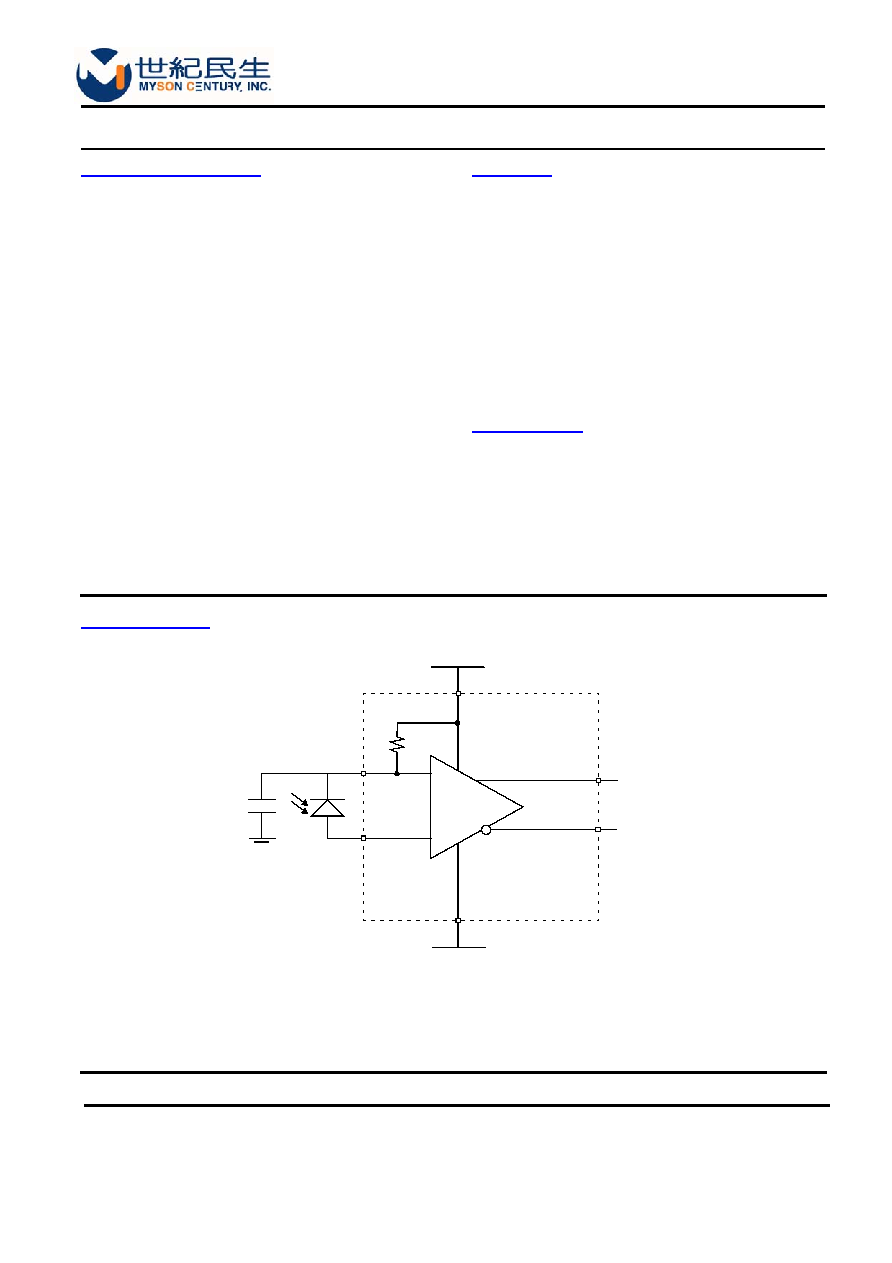
The CS6704 is a first-generation transimpedance
amplifier with AGC designed for STM8/OC-24 fiber
optic systems. The AGC function allows 0dBm input
overload.
The CS6704 amplifies the current generated by a
PIN diode or avalanche photodiode and converts this
to a differential output voltage.
The PINK output of the CS6704 is connected to
V
CC
through a 1.2k
on-chip resistor. By using a
bypass capacitor at this pin, a filter function
significantly reduces the amount of noise at the
cathode of the photodiode.
∑ 3.3V and 5V operation.
∑ 3k
differential transimpedance gain.
∑ 950MHz bandwidth
∑ On-chip Automatic Gain Control (AGC).
∑ Differential outputs.
∑ Available as die.
∑ 0 dBm overload.
V
CC
GND
DOUTP
PINA
PINK
DOUTN
CS6704
470pF
∑ Fiber Channel
∑ SDH/SONET
∑ Gigabit Ethernet
*This datasheet is the confidential information of MYSON CENTURY, INC. and is subject to various privileges
against unauthorized disclosure. Recipient shall not disclose this confidential information to any other person,
nor shall one use the confidential information for the purpose of competing with MYSON CENTURY, INC.
CONFIDENTIAL
page 2 of 6
CS6704
Preliminary
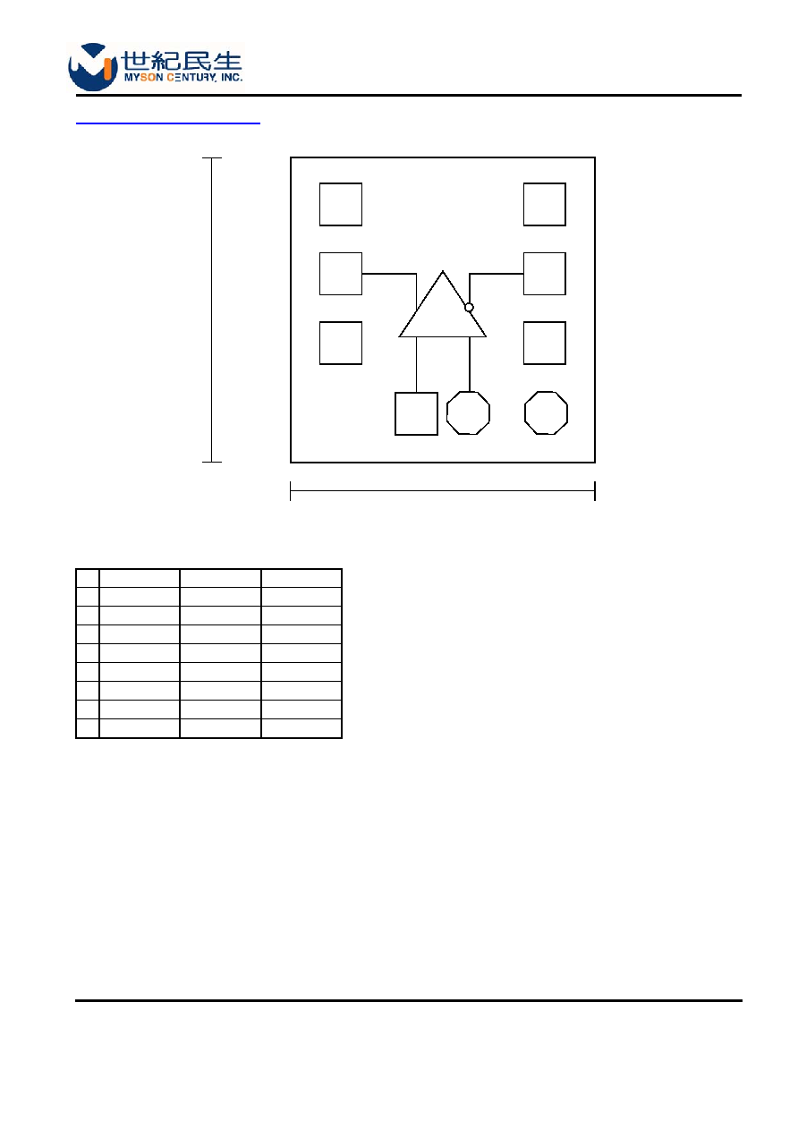
PIN CONNECTION DIAGRAM
Figure-1
Note: The coordinates start from the center of PAD PINK to the center of each PAD, and the total die size does not include
seal ring and scribe line.
1
GND
X=0
Y=523.4
2
DOUTP
X=0
Y=373.4
3
V
CC
X=0
Y=0
4
PINK
X=216.05
Y=-90.3
5
PINA
X=505.95
Y=-98.3
6
VH
X=704
Y=-100.25
7
V
CC
X=704
Y=0
8
DOUTN
X=704
Y=373.4
9
GND
X=704
Y=523.4
1
2
3
4
7
8
9
GND
GND
DOUTP
V
CC
V
CC
DOUTN
VH
803
µ
m
5
6
PINK PINA
1082.2 µ
m
CONFIDENTIAL

page 3 of 6
CS6704
Preliminary
PIN DESCRIPTION
Note: PINA is an ESD sensitive pin. Handle with care.
Name
Pin
Description
GND
1, 9
Ground pin. Connect to most negative supply voltage.
DOUTP
2
Data output pin. This pin goes high when current flows into pin PINA.
V
CC
3, 7
Power pin. Connect to most positive supply voltage.
PINK
4
PIN input pin. Connect the cathode of the photodiode between this pin and PINA. Connect a
capacitor between this pin and ground. Tying this pin to ground to disable the DC Restore
function.
PINA
5
PIN input pin. Connect the anode of the photodiode between this pin and PINK.
VH
6
Test pin. Measure the voltage of this pin can get the transimpedance gain. Leave this pin open in
typical application circuits.
DOUTN
8
Inverting data output pin. Complementary to pin DOUTP.
CONFIDENTIAL

page 4 of 6
CS6704
Preliminary
FUNCTIONAL DESCRIPTION
The CS6704 is a transimpedance pre-amplifier fabricated by BiCMOS process. The CS6704 consists of a
transimpedance amplifier, an AGC control block, an output buffer, a DC restore block, and a voltage regulator.
Transimpedance Amplifier
The transimpedance amplifier in CS6704 is a high gain, single ended amplifier with a feedback resistor. The
feedback resistor converts the input current to a voltage at the output node, and is controlled by the AGC control
block. The minimum differential output swing is 10mV with 50
load at -27dBm input.
AGC Control Block
The AGC control block is to prevent the output voltage swing from saturation. When the input optic power is lower
than -9.5dBm, the AGC function is disabled, and the transimpedance gain is 3.2k
.
Output Buffer
The single-ended output of transimpedance amplifier is converted to differential signal through output buffer. It is
able to drive either a 50
load or a high impedance load. The output swing will be smaller when the CS6704 is
terminated with a 50
load. For better noise rejection, the different output should be terminated symmetrically.
DC Restore Block
The DC restore block draws DC component of the input current, thus minimize the pulse width distortion of large
input current.
Voltage Regulator
In order to minimize the influence of power supply on noise performance, a voltage regulator is incorporated in
the CS6704.
CONFIDENTIAL
