 | –≠–ª–µ–∫—Ç—Ä–æ–Ω–Ω—ã–π –∫–æ–º–ø–æ–Ω–µ–Ω—Ç: MTD214 | –°–∫–∞—á–∞—Ç—å:  PDF PDF  ZIP ZIP |
MYSON
TECHNOLOGY
MTD214
Ethernet Encoder/Decoder and 10BaseT
Transceiver with Built-in Waveform Shaper
This datasheet contains new product information. Myson Technology reserves the rights to modify the product specification without notice.
No liability is assumed as a result of the use of this product. No rights under any patent accompany the sale of the product.
MTD214 Revision 1.4 1205/1997
1/11
FEATURES
∑
Compatible with IEEE 802.3 standards.
∑
Built-in UTP output waveform shaping function.
∑
Selectable media interface and auto-detection functions.
∑
Automatic polarity detection and correction.
∑
Link status output.
∑
Heartbeat disable/enable selection.
∑
Support full-duplex operation.
∑
Standard 802.3 AUI interface.
∑
Selectable controller interface.
∑
Low power consumption.
GENERAL DESCRIPTION
MTD214 contains integrated functions of the Ethernet encoder/decoder and UTP/AUI interface. The
encoder/decoder conforms to IEEE 802.3 protocol and performance requirements while also retaining
compatibility with most popular network controllers. The UTP transceiver has a built-in waveform shaping
function thus eliminating the requirement of an external filter. The transceiver also contains the functions of
automatic media selection and polarity correction. MTD214 is available in 28-pin plastic DIP (600mil) or SOJ
(300mil) packages.
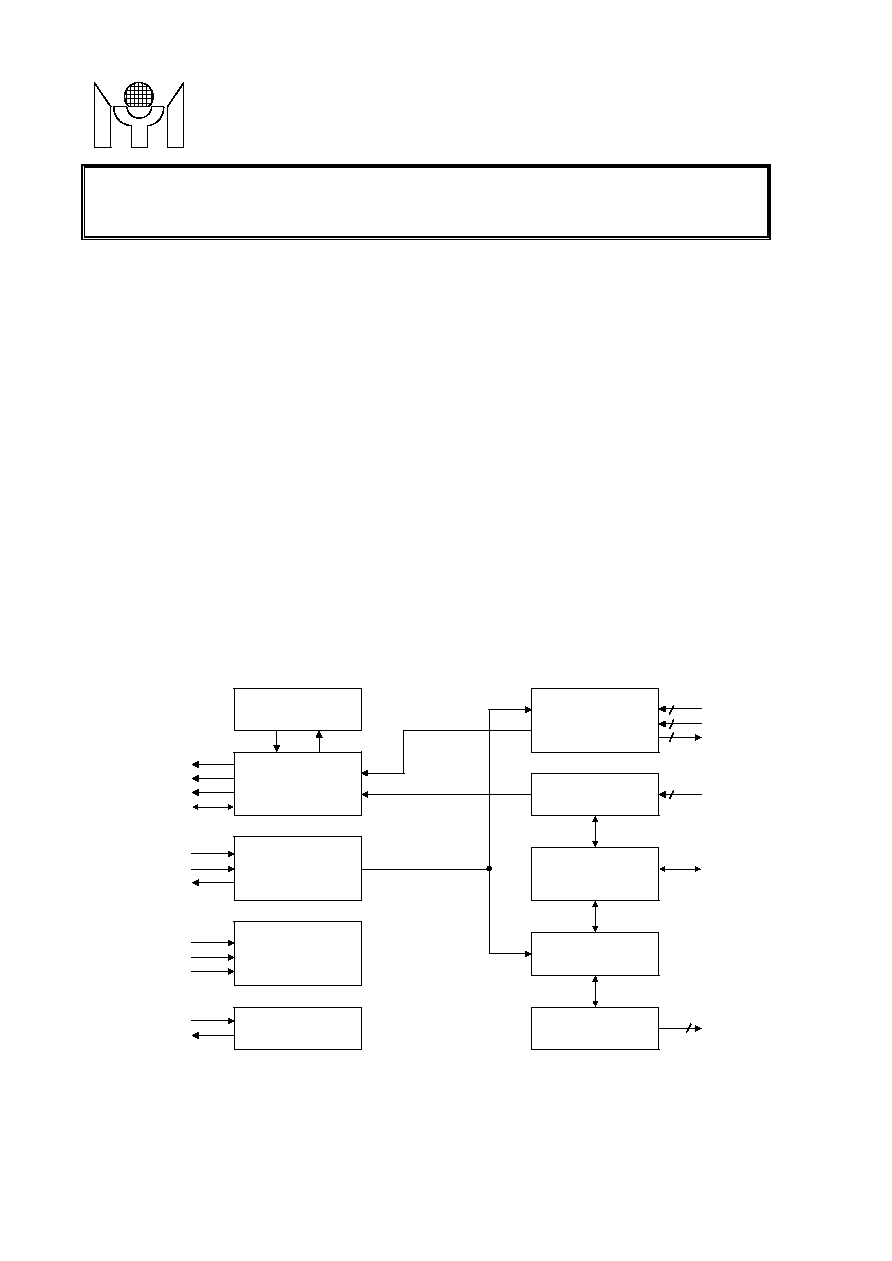
BLOCK DIAGRAM
VCO/PLL
MANCHESTER
DECODER
MANCHESTER
ENCODER
CONTROL
REFERENCE
CLOCK
AUI
UTP RECEIVE
LINK TEST/
JABBER
UTP TRANSMIT
OUTPUT
DRIVER
CRS
RXC
RXD
COL/HBE
TXE
TXD
TXC
NIS
CIS
FDX
X1
X2
DIP/DIN
CIP/CIN
DOP/DON
2
2
2
TPIP/TPIN
2
LTE/LS
TPOP/
TPON
2

MYSON
TECHNOLOGY
MTD214
MTD214 Revision 1.4 12/05/1997
2/11
1.0 CONNECTION DIAGRAM
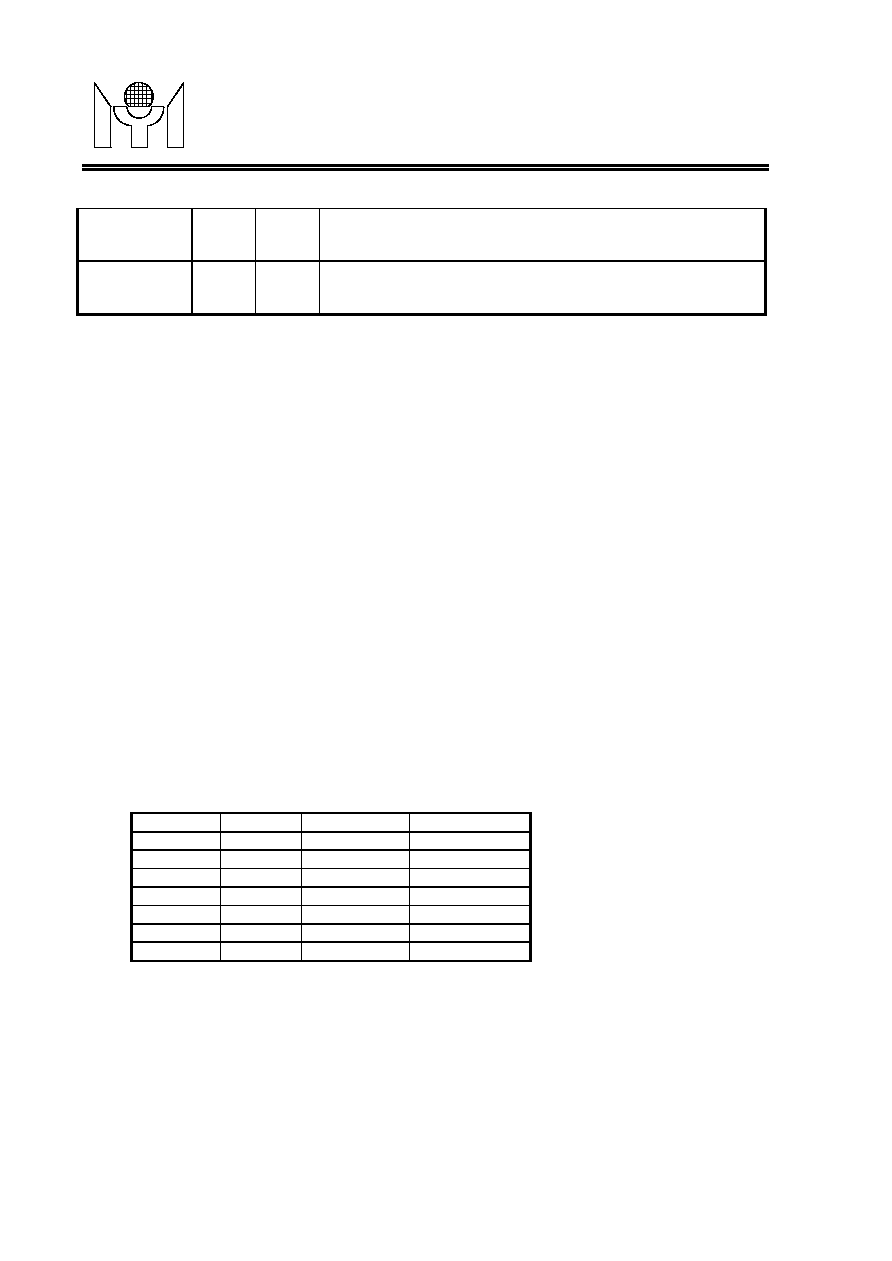
2.0 PIN DESCRIPTIONS
Name
I/O
Pin #
Descriptions
GNDA
P
1
Ground for analog and internal circuits.
VDDA
P
2
+5V (+/-5%) supply for internal circuits.
COL/HBE
I/O
3
Collision detection output connecting to the network controller.
This pin is also an input pin that determines the heartbeat
function. During reset period, COL output is disabled, and input is
latched to control the heartbeat function. After reset, COL is
asserted when a collision is sensed on the network, during
heartbeat period or jabber condition.
RXD
O
4
Receives data output connecting to the network controller. RXD is
the decoded NRZ data from the network.
CRS
O
5
Carrier sense output connecting to the network controller. CRS is
asserted when there is activity on the media, and is de-asserted
by the end of the packet condition on the media. It is also de-
asserted if loss of SYNC condition occurs during the reception of
the packets.
RXC
O
6
Receives clock output connecting to the network controller. RXC
is derived from the Manchester data on the received data. In
NS/AMD mode, it is active only during packet reception. In
Intel/AT&T mode, it is continuous following the TXC clocks during
idle period and switched to the received clocks as the packet
arrives.

MYSON
TECHNOLOGY
MTD214
MTD214 Revision 1.4 12/05/1997
3/11
LTE/LS
I/O
7
Test enabler and status links. This is a dual-purpose pin. It is an
input that occurs during the power-on reset period. If MTD214
senses it is high during reset, MTD214 enables the link test
function of the on-chip UTP transceiver and outputs the link status
through this pin. To disable the link test function, this pin should
be forced below 1.5 V during reset. Note that MTD214 always
outputs the link pulses independent of the link test.
CIS
I
8
Controller interface selection. This pin selects the signal format of
the ENDEC output. If it is high, the format conforms to the
Intel/AT&T controller. If it is low, it conforms to NS/AMD format.
NIS
I
9
Media interface selection. This pin selects the network media. If it
is high, the on-chip UTP transceiver is selected. If it is low, AUI is
selected. It is also combined with the FDX pin to define the
loopback test mode. Please see the functional description for the
mode table.
X1/X2
I
10,11
Crystal oscillator. A 20MHz-30pF with 100ppm accuracy crystal
should be mounted between these 2 pins as well as two 30pF
+/- 5% capacitors connecting each pin to ground. If an external
clock source is used, it should be applied through X1 and allow X2
to be grounded.
TXD
I
12
Transmitted data input connected to the network controller. The
data is in NRZ format and is gated by the TXE signal.
TXC
O
13
Transmitted clock output connected to the network controller.
This is a 10MHz clock used to synchronize TXE and TXD.
TXE
l
14
Transmitted enabler input connected to the network controller.
This signal is used by MTD214 to gate the TXD input for packet
transmission.
FDX
I
15
Full duplex mode selection input. When this pin is low, half duplex
and normal Ethernet operation is selected. When this pin is high,
full duplex mode operation is enabled. In this mode, the collision
status reporting is disabled, but heartbeat and jabber conditions
are still reported on the COL pin. Since full duplex mode can be
implemented in UTP media only when MTD214 is in auto media
selection mode, AUI selection precedes the priority of full duplex
mode. This pin is also combined with the NIS pin to define various
testing modes of MTD214.
GNDO
P
17
Ground for UTP output transmitter.
TPOP/TPON
O
18,16
UTP transmitted output connected to an output transformer that
couples with the UTP cable. The transformer should have an
inductance of 100 to 200 uH and 1:1 turn ratio. Two 50-Ohm load
resistors should also connect each output to VDD as load
resistors. It is also recommended that a 100pF capacitor be
connected to this pin from ground to remove any spurious noise.
GNDD
P
19
Ground for UTP output transmitter and AUI buffer.
VDDD
P
20
+5 V supply for AUI buffer.
DOP/DON
O
22,21
Data output for AUI interface. This differential signal should drive
an equivalent load of 39 Ohm. Typically an external 78 Ohm
connected across these 2 pins and the equivalent remote AUI
load together are used to ensure proper amplitude. The AUI
interface should be transformer-coupled.
CIP/CIN
I
23,24
Collision input for AUI interface. This differential signal is coupled
through the transformer. An external bias of 2.5V should be
applied to these 2 pins.
MYSON
TECHNOLOGY
MTD214
MTD214 Revision 1.4 12/05/1997
4/11
DIP/DIN
I
25,26
Data input for AUI interface. This differential signal is coupled
through the transformer. An external bias of 2.5V should be
applied to these 2 pins.
TPIP/TPIN
I
27,28
UTP receiving input. This differential signal is connected to the
UTP receiving pair through the isolation transformer. An external
bias of 2.5V should be applied to these 2 pins.
3.0 FUNCTIONAL DESCRIPTION
3.1 Manchester Decoder and PLL
The Manchester decoder uses a PLL to extract the clock and NRZ data from the received Manchester signals.
The PLL is locked to the internally generated 5MHz clocks during idle time and switched to the incoming data
at the start of the packet detection. The decoder also detects the IDL condition of the incoming data by
switching off CRS whenever the data stays unchanged longer than 125 nsec.
3.2 Manchester Encoder
The Manchester encoder receives the NRZ data from the controller and converts it into Manchester format
using the internal 20MHz clocks. TXD and TXE must be synchronized by TXC. The encoder also guarantees
that a low transition occurs first at the start of the packet and appends the IDL at the end of the transmitted
data.
3.3 Reference and Clock
An internal bandgap circuit is used to generate all necessary reference voltages and currents. The on-chip
crystal oscillator is used to generate 20MHz reference clocks for the internal circuits. For precision clock
generation, a 20MHz-30 100ppm crystal should be used. And two 30pF load capacitors should be connected
from X1 and X2 to ground, respectively. If an external clock source is used, it should be applied to X1 while X2
is grounded.
3.4 Control Function
This block controls the operating mode of MTD214. The CIS pin controls the type of controller interface. When
CIS is high, MTD214 is in Intel/AT&T mode; when CIS is low, MTD214 is in NS/AMD mode. Do not allow this
pin to float. NIS and FDX pins determine the operation mode according to the following table:
FDX
NIS
MODE
MEDIA
0
0
Half
AUI
0
1
Half
UTP
0
F
Half
Auto detect
1
0
Loopback
N/A
1
1
Full
UTP
1
F
Full/Half
Auto UTP/AUI
F
X
Test Mode
Note that full duplex mode is meaningful only if the media selection is UTP. Thus if MTD214 is configured as
auto media switching, the full duplex is switched back to half duplex if AUI is selected. Also if the link test
function is disabled (LTE=0), MTD214 assumes that the link test pass state and UTP are always selected if
configured in auto detection mode. In full duplex mode, collision reporting is disabled and internal loopback of
UTP transmission data is also inhibited. However, heartbeat and jabber functions of the on-chip UTP
transceiver are still effective.
3.5 UTP Receiving
A low-pass filter is used to filter the noise in the received UTP differential signals. The common-mode level of
the differential signal is extracted and is used for DC squelch circuits. AC squelch circuits reject any single

MYSON
TECHNOLOGY
MTD214
MTD214 Revision 1.4 12/05/1997
5/11
cycle signals between 3MHz and 15 MHz as well as continuous signals below 2.5MHz. The squelch circuit also
recognizes the link pulses. Once the squelch is off, the differential signal is amplified to logic levels. There is no
internal bias of TPIP and TPIN signals; an external bias (2.5V) should be applied to these inputs through the
termination resistors.
3.6 Link Test and Jabber Logic
The link test circuit performs the necessary link test functions specified by IEEE 802.3. The link test function is
enabled when LTE/LS is sampled high during reset period. If the link test function is enabled, the LTE/LS pin
becomes an output that can drive the link LED display. To disable the link test function, LTE should be tied low.
The link test function can be changed only by power-on and off. Note that if the link test is disabled, the
generation of link pulses is not affected. The link test status is used to control the on-chip UTP transceiver and
the media selection. If the link test fails, and auto detection mode is enabled, the media is set to AUI. The link
test circuit also includes the polarity detection function. Detection is based on the polarity of received link
pulses. If 8 consecutive reversed link pulses are received, the polarity is toggled. The jabber logic monitors the
length of the continuous transmission time. If the transmission time exceeds the maximum jabber time, the
transmission is disabled and COL is asserted to indicate the jabber status. In addition, the logic implements the
heartbeat function. The heartbeat enable signal is latched during reset period from the COL pin. To enable the
heartbeat function, an external pull-up resistor of 4.7K Ohms should be connected to the COL pin. To disable
the heartbeat function, a pull-down resistor should be used.
3.7 UTP Transmission and Output Driver
The UTP transmission circuit takes the Manchester decoded data and converts it into a coded format that
meets IEEE 802.3-required transmission templates. The coded data is fed into an oversampling D/A and filters
for waveform shaping. The output buffer of the transmitter is an open-drain type current source. The output
voltage of the transmitter is developed on the external load resistors (50 Ohm) connected to the power supply.
The output should be transformer-coupled to the UTP media.
3.8 AUI Interface
The AUI interface consists of CI/DI squelch detection and receiving circuits, and a DO output driver. The CI/ DI
inputs should be externally biased at 2.5V through the termination resistors, and transformer-coupled to the
AUI media. The DO output is a push-pull driver. The output should have an equivalent load of 39 Ohm to
ensure proper amplitude. AUI media is selected either by setting NIS low or in auto switching mode with link
fail conditions.
4.0 ELECTRICAL CHARACTERISTICS
4.1 DC Characteristics Ta = 0C to 70 C, VDD = 5V +/- 5%, Vss = 0V
Parameter
Symbol
Min
Typ
Max
Unit
Note
Supply current
Idle
Traffic
Idd, idle
Idd, traf
-
-
20
30
30
40
mA
mA
Input low voltage (digital inputs)
VIL
-0.3
-
0.8
V
Input high voltage (digital inputs)
VIH
2.4
-
Vdd+0.3
V
Input high current (digital inputs)
IIH
-
-
100
uA
Input low current (digital inputs)
IIL
-
-
100
uA
Output low voltage (digital outputs/w
IOL=4mA)
VOL
-
0.5
0.8
V
Output high voltage (digital outputs/w
IOH=500uA)
VOH
3.0
3.5
-
V
AUI output differential voltage
(DOP,DON)
VOD
+/-500
-
+/-1500
mV
1
AUI idle offset voltage
VAI
-
0
+/-40
mV
AUI input squelch voltage
VAS
-175
-250
-300
mV
2

MYSON
TECHNOLOGY
MTD214
MTD214 Revision 1.4 12/05/1997
6/11
(DIP,DIN,CIP,CIN)
UTP input squelch voltage
(TPIP,TPIP)
VTS
+/-200
+/-250
+/-300
mV
Analog input common voltage
(DIP,DIN,CIP,CIN,TPIP,TPIN)
VAC
1.5
2.5
3.5
V
UTP peak output voltage
(TPOP,TPON)
VTO
+/-2.0
+/-2.5
+/-3.0
V
3
4.2 Switching Characteristics
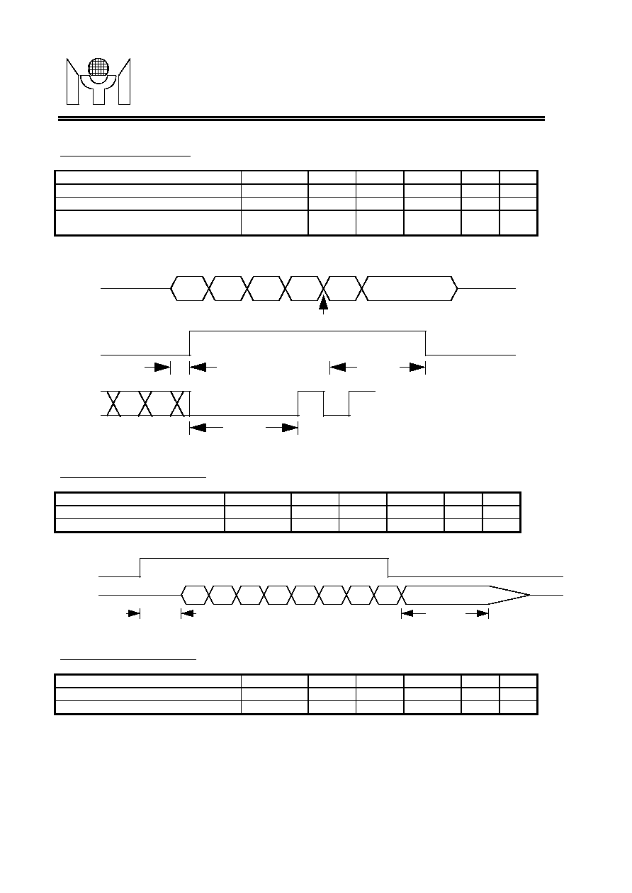
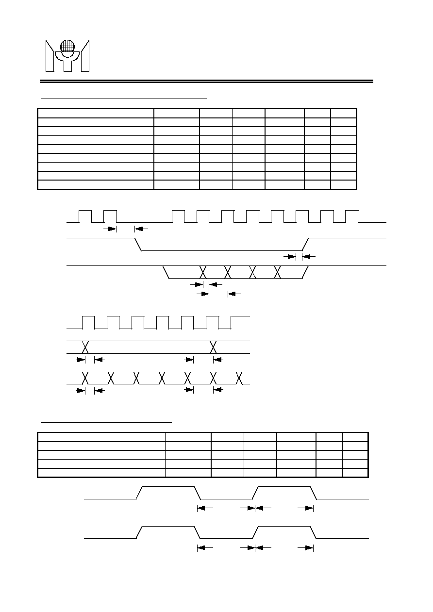
4.2.1 TP Reception Timing
Parameter
Symbol
Min
Typ
Max
Unit
Note
TP active to CRS assertion
tTPVCSH
-
300
350
ns
TP active to RXC validation
tTPVRCH
-
9
11
BT
TP end of packet detection (from bit
boundary)
tTPHCSL
100
125
170
ns
TPI
RECEIVE START OF PACKET
RECEIVE END OF PACKET
Bit Boundary
IDL
tTPHCSL
tTPVCSH
CRS
RXC
tTPVRCH
Figure 1. TP Reception Timing
4.2.2 TP Transmission Timing
Parameter
Symbol
Min
Typ
Max
Unit
Note
TXE to TP output
tTNHPOX
-
100
150
ns
TXE to CRS loopback
tTNHCSH
-
150
200
ns
TXE to RXC loopback
tTNHRCC
-
8
10
BT
TP end of packet IDL width
tPOHPOL
250
275
300
ns

MYSON
TECHNOLOGY
MTD214
MTD214 Revision 1.4 12/05/1997
7/11
RXC
tTNHRCV
CRS
tTNHCSH
TPO
IDL
tPOHPOL
tTNHPOX
TXE
TRANSMIT START OF PACKET
TRANSMIT END OF PACKET
Fig
ure 2. TP Transmission Timing
4.2.3 TP Collision Timing
Parameter
Symbol
Min
Typ
Max
Unit
Note
TPI to COL assertion
tTPVCLH
-
300
400
ns
TPI to COL de-assertion
tTPHCLL
-
125
200
ns
TXE to COL assertion
tTNHCLH
-
125
200
ns
TXE to COL de-assertion
tTNLCCL
-
350
450
ns
TPI
IDL
TXE
TRANSMIT-RECEIVE COLLISION DETECTION
RECEIVE-TRANSMIT COLLISION DETECTION
COL
tTPVCLH
tTPHCLL
tTNHCLH
tCLHCLL
tTNLCLL
Figure 3. TP Collision Timing
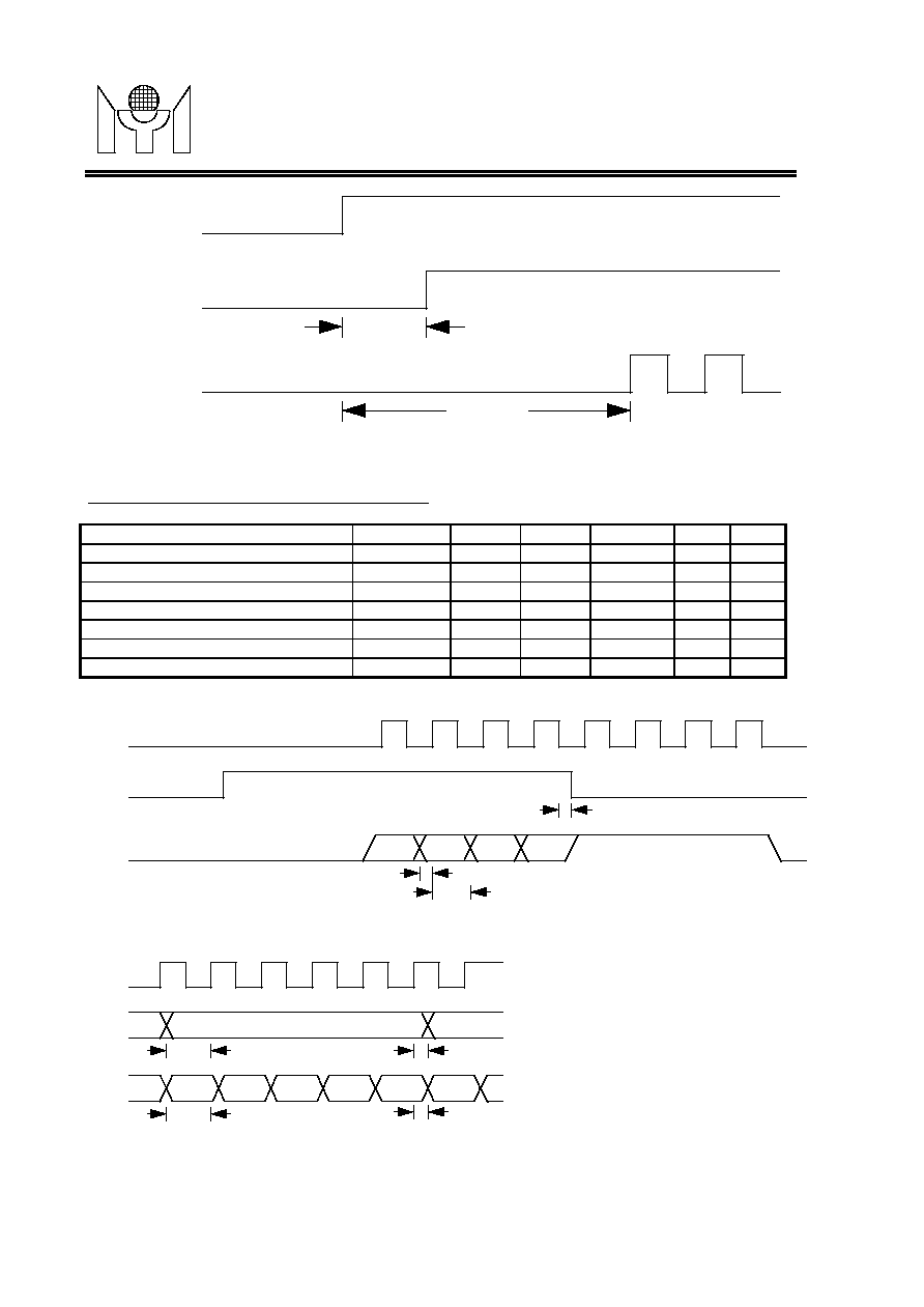
4.2.4 TP HBT and Jabber Timing
Parameter
Symbol
Min
Typ
Max
Unit
Note
Heartbeat delay
tTNLCLV
800
1000
1200
ns
Heartbeat duration
tTNLCLL
800
1000
1200
ns
Jabber turn-on time
tTNHCJH
40
45
55
ms
Jabber reset time
tTNHCJL
250
500
750
ms
TPO
TXE
COL
tTNLCLV
tTNHCJH
tTNLCJL
Figure 4. TP HBT and Jabber Timing
MYSON
TECHNOLOGY
MTD214
MTD214 Revision 1.4 12/05/1997
8/11
4.2.5 AUI Reception Timing
Parameter
Symbol
Min
Typ
Max
Unit
Note
DI active to CRS assertion
tDIVCSH
-
40
80
ns
DI active to RXC validation
tDIVRCH
-
4
6
BT
DI end of packet detection (from bit
boundary)
tDIHCSL
100
125
170
ns
Bit Boundary
DI
RECEIVE START OF PACKET
RECEIVE END OF PACKET
IDL
CRS
tDIVCSH
tDIHCSL
RXC
tDIVRCH
Figure 5. AUI Reception Timing
4.2.6 AUI Transmission Timing
Parameter
Symbol
Min
Typ
Max
Unit
Note
TXE to DO output
tTNHDOX
-
100
150
ns
DO end of packet IDL width
tDOHPOL
250
275
300
ns
TXE
TRANSMIT START OF PACKET
TRANSMIT END OF PACKET
DO
tTNHDOX
tDOHDOL
IDL
Figure 6. AUI Transmission Timing
4.2.7 Local Loopback Timing
Parameter
Symbol
Min
Typ
Max
Unit
Note
TXE to CRS assertion
tTNHCSH
-
60
100
ns
TXE to RXC validation
tTNHRCV
-
6
8
BT
MYSON
TECHNOLOGY
MTD214
MTD214 Revision 1.4 12/05/1997
9/11
TXE
CRS
tTNHCSH
RXC
tTNHRCV
Figure 7. Local Loopback Timing
4.2.8 Controller Interface Timing (NS/AMD Mode)
Parameter
Symbol
Min
Typ
Max
Unit
Note
RXD setup to RXC rising
tRDVRCH
40
55
-
ns
RXD hold after RXC
tRCHRDH
30
45
-
ns
RXC low to CRS de-assertion
tRCLCSL
0
20
50
ns
TXE setup to TXC rising
tTNVTCH
30
-
-
ns
TXD setup to TXC rising
tTDVTCH
30
-
-
ns
TXE hold after TXC
tTCHTNH
0
-
-
ns
TXD hold after TXC
tTCHTDH
0
-
-
ns
START OF PACKET
END OF PACKET
RXC
CRS
tRCLCSL
RXD
tRDVRCH
tRCHRDH
Receive
Transmit
TXC
TXE
tTNVTCH
tTCHTNH
TXD
tTDVTCH
tTCHTDH
Fig
ure 8. Controller Interface Timing (NS/AMD Mode)
MYSON
TECHNOLOGY
MTD214
MTD214 Revision 1.4 12/05/1997
10/11
4.2.9 Controller Interface Timing (Intel/AT&T Mode)
Parameter
Symbol
Min
Typ
Max
Unit
Note
RXC to CRS assertion
tRCLCSL
0
70
100
ns
RXD setup to RXC fall
tRDVRCL
40
55
-
ns
RXD hold after RXC
tRCLRDH
30
45
-
ns
RXC high to CRS de-assertion
tRCHCSH
0
20
50
ns
TXE setup to TXC fall
tTNVTCL
30
-
-
ns
TXD setup to TXC fall
tTDVTCL
30
-
-
ns
TXE hold after TXC
tTCLTNH
0
-
-
ns
TXD hold after TXC
tTCLTDH
0
-
-
ns
RXC
START OF PACKET
END OF PACKET
tRCLCSL
CRS
tRCHCSH
RXD
tRDVRCL
tRCLRDH
TXC
TXE
tTNVTCL
tTCLTNH
TXD
tTDVTCL
tTCLTDH
Figure 9. Controller Interface Timing (Intel/AT&T Mode)
4.2.10 Specific Timing for RXC and TXC
Parameter
Symbol
Min
Typ
Max
Unit
Note
RXC low width
tRCLRCH
45
50
55
ns
RXC high width
tRCHRCL
45
50
55
ns
TXC low width
tTCLTCH
45
50
55
ns
TXC high width
tTCHTCL
45
50
55
ns
RXC
tRCLRCH
tRCHRCL
TXC
tTCLTCH
tTCHTCL
MYSON
TECHNOLOGY
MTD214
MTD214 Revision 1.4 12/05/1997
11/11
Figure 10. Specific Timing for RXC and TXC
5.0 APPLICATION CIRCUITS
Please see attachment.
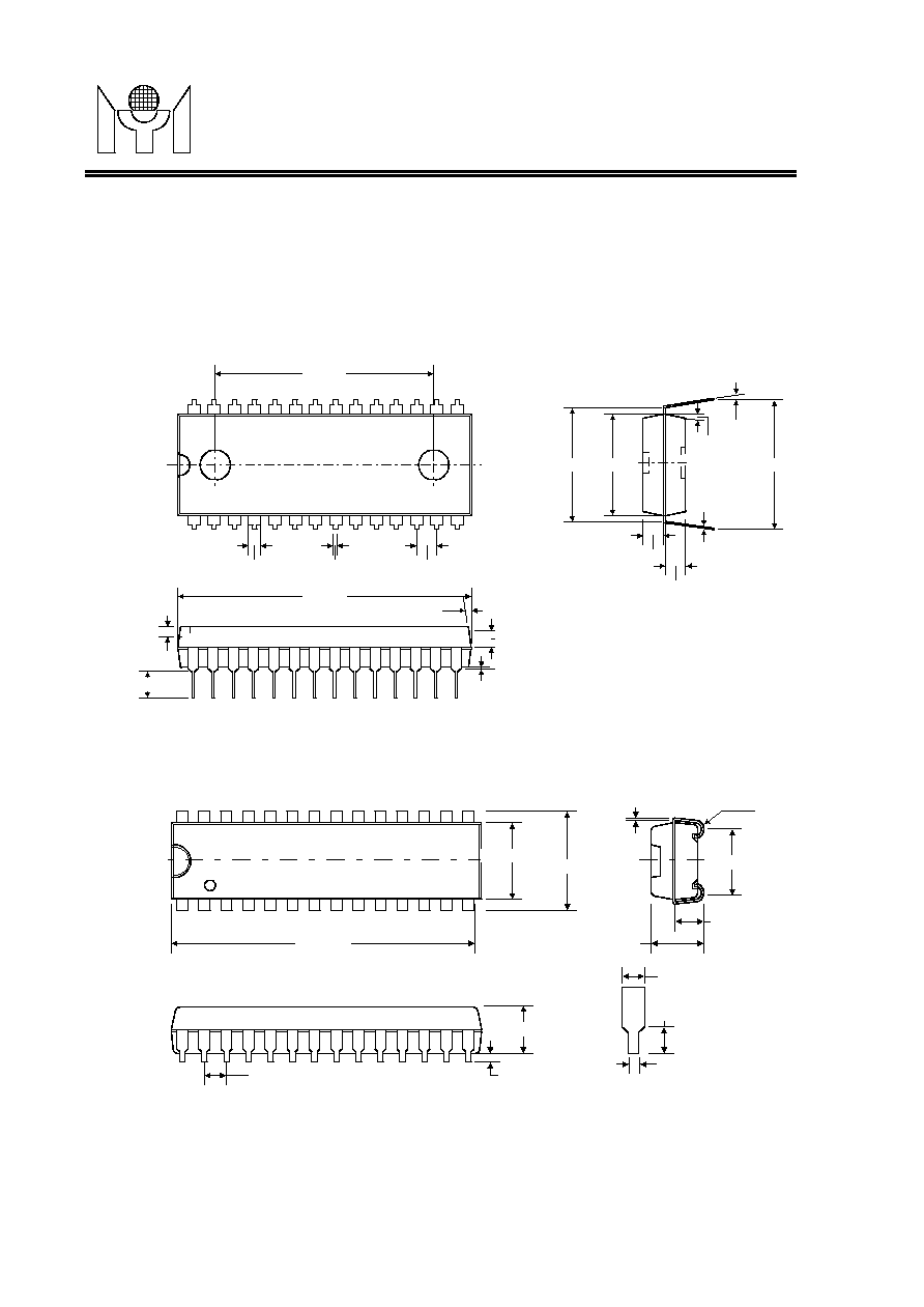
6.0 PACKAGE DIMENSION
A. 600 MIL 28-PIN PDIP
Unit: mil
1540 +/-10
100Typ.
18+/-2Typ.
50Typ.
35+/-5
1.778mm
+/-0.127
0.254mm
(min.)
100Min.
612 +/-12 550 +/-4
650 +/-20
70 +/-4
5
o
~7
0
6
o
+/-3
o
70 +/-4
10
2050 +/-10
7Typ.
B. 300 MIL 28-PIN SOJ
UNIT: INCH
0.725+/-0.01
R0.030"
0.040"
0.267
0.007~0.013
0.025" Min.
0.1 ref
0.050 bsc
0.138 +/-0.01
0.082Min.
0.300 +/-0.005
0.335 bsc
0.05" Max.
0.018 +/-0.002
0.026"/0.032"
28
15
14
1