 | –≠–ª–µ–∫—Ç—Ä–æ–Ω–Ω—ã–π –∫–æ–º–ø–æ–Ω–µ–Ω—Ç: MTD503 | –°–∫–∞—á–∞—Ç—å:  PDF PDF  ZIP ZIP |

GENERAL DESCRIPTION
FEATURES
2-Port Media Converter Switch with PHY
Sales@myson.com.tw
www.myson.com.tw
Rev.0.91 September 2003
page 1 of 37
Myson Century, Inc.
No. 2, Industry East Rd. III,
Science-Based Industrial Park, Hsin-Chu, Taiwan
Tel: 886-3-578-4866 Fax: 886-3-578-4349
MTD503
Preliminary
The MTD503 can be configured to one of the
following modes: embedded mode, external mode,
SW-TX mode, and SW-FX mode. In the embedded
mode, SW engine connects with internal PHYs
directly. In external mode, two internal PHYs are
disabled and the both ports of the SW engine are
connected to MII ports. SW-TX and SW-FX modes
are special. In the SW-TX mode, the connection
between the SW and copper PHY is cut off. They
connect to MII ports. In the SW-FX mode, the
connection between SW and fiber PHY is cut off.
They connect to MII ports. Pin for Far-End-Fault
receiving indication is available in this mode.
Customer-specified Far-End-Fault pattern is
possible. With these special functions and
configurations, customers can add specific fiber
control logic in the SW-FX mode.
*This datasheet is the confidential information of MYSON CENTURY, INC. and is subject to various privileges
against unauthorized disclosure. Recipient shall not disclose this confidential information to any other person,
nor shall one use the confidential information for the purpose of competing with MYSON CENTURY, INC.
∑ One 10/100Base-TP port and one 100Base-FX
port
∑ Integrated fiber and copper Ethernet PHY, frame
buffer, and switch engine
∑ IEEE 802.3u compliant
∑ Auto negotiation for TP port
∑ 26KX2 independent linear frame buffer
∑ 1KX2 MAC address look-up
∑ Automatic MAC address learning, address aging,
and frame filtering
∑ 802.3x flow control in full duplex mode
∑ Backpressure in half duplex mode
∑ Additional two MII and one SMI ports
∑ Configurable MII ports for switch engine, fiber PHY
and copper PHY
∑ Link pass through
∑ Cut through
∑ Loop back at PHY MII or MAC MII
∑ Customer specific OAM packet receiving and
transmission
∑ Customer specific maximum packet size up to
9216 bytes
∑ Customer specific Far-End-Fault Indication pattern
∑ Support jumbo frame and VLAN frame
∑ 128-pin PQFP package
The MTD503 targets at media converter
applications. It performs 100Base-FX to 100/10Base-
Tx data conversion. The speed and duplex mode of
the copper port is determined by one of the three
ways: auto negotiation, set by MII register, and set by
pins. The MTD503 is capable of exchanging data
between 100Mbps and 10Mbps network.
Backpressure and 802.3x flow control are supported.
Once buffer is near full, the MTD503 can issue the
PAUSE frame if the flow control is enabled under full
duplex mode operation. In the case of buffer near full
under half duplex mode, the MTD503 asserts jam
pattern to collide the coming packet. The learning
module records the SA in MAC address table and the
filtering module checks the DA of every receiving
packet. The learning module can record 1024 SA in
maximum for each port. If the received packet is
identified as a local one, the MTD503 drops it to
increase the network performance.
The MTD503 supports OAM packet transmission
and receiving. The OAM packet is a customer
specified, non-Ethernet packet. 4 to 16 bytes packet
length is allowed. The OAM RX/TX module locates
between fiber PHY and switch engine. It is
responsible for OAM packet transmission and
receiving. An external uP is required for
communicating with the OAM module. It reads/writes
the OAM packet, controls the OAM module, and
checks the OAM module status through the serial
management interface. TS-1000 OAM packet is
acceptable by the MTD503.
The MTD503 provides 4 types of loop back routes.
The loop back packet can come from fiber port or
copper port. It can travel across frame buffer then
turn back or directly turn back to PHY without
travelling through the frame buffer. The loop back
mode is activated by an external CPU or uP. In TS-
1000, the uP or CPU enables the loop back mode
after receiving the loop back test OAM packet.
The MTD503 provides functional options. The
maximum normal packet size, maximum VLAN
packet size, maximum jumbo packet size, and buffer-
full threshold can be re-defined through the
EEPROM or registers. The flow control, frame length
checking, jumbo supporting, VLAN supporting,
learning/aging, and CRC checking, MDIX, link pass-
through, cut through can all be enabled or disabled
by setting the optional pins, EEPROM, or registers.
CONFIDENTIAL

BLOCK DIAGRAM
page 2 of 37
APPLICATIONS
MTD503
Preliminary
Reset &
Clock
RSTB,
XI, XO,
CLK_0
FOP0, FON0
SDP0, SDN0
PHYSEL0,
PHYSEL1,
ANEN1,
OPSEL1,
OPTSPD,
OPTFULL
LEDACT0,
LEDACT1,
LEDCOL1
FIP0, FIN0
Fiber
PHY
Configuration
LED Driver
OAM
Packet
TX/RX
OAM
buffer
Port0 MUX
SW engine
Frame buffer
Port1 MUX
Port status
Copper PHY
EEPROM IF
Serial
management
I/F
RXD0_0, RXD1_0, RXD2_0, RXD3_0, CRS0,
RXDV0, RXC0, LNK0, RXER0, FULL0, COL0,
SPD0, TXEN0, TXC0, TXDO_0, TXD1_0, TXD2_0, TXD3_0
RXD0_1, RXD1_1, RXD2_1, RXD3_0, CRS1,
RXDV1, RXC1, LNK1, RXER1, FULL1, COL1,
SPD1, TXEN1, TXC1, TXD0_1, TXD1_1, TXD2_1, TXD3_1
SPDSTS0,
FULLSTS0,
LNKSTS0,
SPDSTS1,
FULLSTS1,
LNKSTS1
TXOP1,TXON1
TXIP1,TXIN1
EEDI
EECK, EEDO
EECS
MDC
MDIO
INT
Fiber to TP Conversion
Fiber Module
MTD503
Fiber RX
Fiber TX
TP TX
TP RX
Transformer
CONFIDENTIAL

Applications (continued)
page 3 of 37
MTD503
Preliminary
Fiber to TP Conversion with Customer Fiber Control
Japanese FTTH with TS-1000
Fiber to TP Conversion with Customer Control and Fiber PHY
Fiber Module
MTD503
Fiber RX
Fiber TX
TP TX
TP RX
Transformer
Customer
Logic
MII
MII
Fiber Module
MTD503
Fiber RX
Fiber TX
TP TX
TP RX
Transformer
CPU/uP
MDC
MDIO
Fiber Module
Customer
RX
TX
MII RX
MII TX
TP TX
TP RX
Transformer
Logic + PHY
MTD503
CONFIDENTIAL
page 4 of 37
MTD503
Preliminary
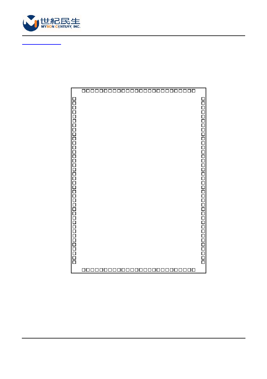
PIN CONNECTION
Figure-1
39
40
41
42
43
44
45
46
47
48
49
50
51
52
53
54
55
56
57
58
59
60
61
62
63
64
1
2
3
4
5
6
7
8
9
10
11
12
13
14
15
16
17
18
19
20
21
22
23
24
25
26
27
28
29
30
31
32
33
34
35
36
37
38
128
127
126
125
124
123
122
121
120
11
9
11
8
11
7
11
6
11
5
11
4
11
3
11
2
111
11
0
109
108
107
106
905
104
103
102
101
100
99
98
97
96
95
94
93
92
91
90
89
88
87
86
85
84
83
82
81
80
79
78
77
76
75
74
73
72
71
70
69
68
67
66
65
RXD0_0
RXD1_0
RXD2_0
RXD3_0
SPD0
GND_M
VCC_M
VCC_P
GND_P
FULL1
LNK1
CRS1
COL1
TXD3_1
TXD2_1
VCC_P
GND_P
TXD1_1
DTX0_1
TXEN1
TXC1
VCC_C
GND_C
RXER1
RXC1
GND_C
VCC_C
VCC_P
GND_P
RXDV1
RXD0_1
RXD1_1
RXD2_1
RXD3_1
SPD1
TESTMODE0
TESTM0DE1
DVDD
VCC_P
GND_P
LNKSTS0
SPDSTS1
FULLSTS1
LNKSTS1
GND_M
VCC_M
INT
CLK_O
VCC_P
GND_P
EECS
EECK
EEDI
EEDO
RSTB
GND_C
XI
XO
VCC_C
VCC_P
OPTFULL
GND_P
GNDPLL
VAAPLL
OPTSPD
PHYSEL1
OPSEL1
GNDT
ANEN1
PHYSEL0
MDIXSET
NC
VAAT
VAAT
TXON1
TXOP1
DVSS
V
SSA
3
VDD
A
3
FO
P0
FO
N
0
V
SSA
2
VDD
A
2
SDN0
SD
P0
FIN0
FI
P
0
VDD
A
1
V
SSA
1
GNDCR
V
VA
A
C
R
V
V
A
AEQ
RXIN1
RXIP1
V
A
AEQ
G
NDEQ
G
NDEQ
GNDREF
RIBB
V
A
AREF
RBIAS_REF
G
NDT
RXDV0
G
ND_P
VCC_P
RXC0
RXER
0
TX
CO
T
XEN0
TXD0_0
G
ND_P
VCC_P
TXD1_0
TXD2_0
TXD3_0
CO
L
0
CRS0
LNK0
FU
LL0
G
ND_P
VCC_P
LEDCO
L1
LEDACT
1
LEDACT
0
MDC
MDIO
SP
DST
S
0
F
U
L
L
ST
S0
MTD503
CONFIDENTIAL

page 5 of 37
MTD503
Preliminary
PIN DESCRIPTION
Name
I/O
Pin No.
Desription
Embedded/External/SW-FX Mode
SW-TX Mode
Port0 MII Interface
RXD0_0
I
1
Port0 MII RXD[0]
Copper PHY TXD[0]
RXD1_0
I
2
Port0 MII RXD[1]
Copper PHY TXD[1]
RXD2_0
I
3
Port0 MII RXD[2]
Copper PHY TXD[2]
RXD3_0
I
4
Port0 MII RXD[3]
Copper PHY TXD[3]
RXC0
I/O
125
Port0 MII RX clock
Copper PHY RXC
RXDV0
I
128
Port0 MII RX data valid
Copper PHY TXEN
RXER0
I/O
124
Port0 MII RX data error
Copper PHY RXER
CRS0
I/O
114
Port0 MII carrier sense
Copper PHY CRS
COL0
I/O
115
Port0 MII collision
Copper PHY COL
TXD0_0
I/O, D
121
Port0 MII TXD[0]
Copper PHY RXD[0]
TXD1_0
I/O, D
118
Port0 MII TXD[1]
Copper PHY RXD[1]
TXD2_0
I/O, D
117
Port0 MII TXD[2]
Copper PHY RXD[2]
TXD3_0
I/O, D
116
Port0 MII TXD[3]
Copper PHY RXD[3]
TXC0
I/O
123
Port0 MII TXD clock
Copper PHY TXC
TXEN0
I/O, D
122
Port0 MII TXD enable
Copper PHY RXDV
SPD0
I
5
Port0 speed
Copper PHY SPD. 0: 100M; 1:10M.
FULL0
I
112
Port0 full duplex/half duplex
Copper PHY FULL. 0: full; 1: half.
LNK0
I/O
113
Port0 link
Copper PHY LINK. 0: link up; 1: link
down.
Port1 MII Interface
RXD0_1
I
31
Port1 MII RXD[0]
Fiber PHY TXD[0]
RXD1_1
I
32
Port1 MII RXD[1]
Fiber PHY TXD[1]
RXD2_1
I
33
Port1 MII RXD[2]
Fiber PHY TXD[2]
RXD3_1
I
34
Port1 MII RXD[3]
Fiber PHY TXD[3]
RXC1
I/O
25
Port1 MII RX clock
Fiber PHY RXC
RXDV1
I
30
Port1 MII RX data valid
Fiber PHY TXEN
RXER1
I/O
24
Port1 MII RX data error
Fiber PHY RXER. RXD[4] in 5B
mode.
CRS1
I/O
12
Port1 MII carrier sense
Fiber PHY CRS
COL1
I/O
13
Port1 MII collision
Fiber PHY received standard FEFI
TXD0_1
I/O, D
19
Port1 MII TXD[0]
Fiber PHY RXD[0]
TXD1_1
I/O, D
18
Port1 MII TXD[1]
Fiber PHY RXD[1]
TXD2_1
I/O, D
15
Port1 MII TXD[2]
Fiber PHY RXD[2]
CONFIDENTIAL

page 6 of 37
MTD503
Preliminary
TXD3_1
I/O, D
14
Port1 MII TXD[3]
Fiber PHY RXD[3]
TXC1
I/O
21
Port1 MII TXD clock
Fiber PHY TXC
TXEN1
I/O, D
20
Port1 MII TXD enable
Fiber PHY RXDV
SPD1
I
35
Port1 speed
5B mode enable
FULL1
I
10
Port1 full duplex/half duplex
TXD[4] in SW-FX mode
LNK1
I/O
11
Port1 link
Fiber PHY LINK. 0: link up; 1: link
down.
Port0 LED
LEDACT0
I/O, D
107
Port0 activity LED. When link on, output low. When TX or RX, toggle.
Port1 LED
LEDACT1
I/O, D
108
Port1 activity. When link on, output low. When TX or RX, toggle.
LEDCOL1
I/O, D
109
Port1 collision LED. In full, output low. In half and collision, toggle.
PHY's Mode Setting
PHYSEL0
I, D
71
Fiber PHY selection. 0: internal PHY; 1: external PHY.
ANEN1
I, U
72
Copper PHY auto negotiation enable. 0: disable; 1: enable.
OPSEL1
I, D
74
Copper PHY force mode selection. 0: forced by pin; 1: forced by MII register.
Available only when ANEN1=0.
PHYSEL1
I, D
75
Copper PHY selection. 0: internal PHY; 1: external PHY.
OPTSPD
I, D
76
Internal PHY speed setting. In SW-FX mode, set TX PHY. 0: 100M; 1: 10M. No
use in other modes.
OPTFULL
I, D
80
Internal PHY duplex setting. In SW-FX mode, set TX PHY. 0: full; 1: half. No
use in other modes.
Port Status
SPDSTS0
I/O, D
104
Port0 speed status. 0: 100M; 1: 10M.
FULLSTS0
I/O, D
103
Port0 mode status. 0: full duplex; 1: half duplex.
LNKSTS0
I/O, D
100
Port0 link status. 0: link up; 1: link down.
SPDSTS1
I/O, D
99
Port1 speed status. 0: 100M; 1: 10M.
FULLSTS1
I/O, D
98
Port1 mode status. 0: full duplex; 1: half duplex.
LNKSTS1
I/O, D
97
Port1 link status. 0: link up; 1: link down.
Clock and Reset
XI
I
84
25MHz crystal input
XO
O
83
25MHz crystal output
Name
I/O
Pin No.
Desription
Embedded/External/SW-FX Mode
SW-TX Mode
CONFIDENTIAL

page 7 of 37
MTD503
Preliminary
RSTB
I
86
System reset. Active low
EEPROM Interface
EECK
I/O, D
89
Serial EEPROM clock
EEDO
I/O, D
87
Data to Serial EEPROM
EEDI
I
88
Data from Serial EEPROM
EECS
O
90
Chip select for Serial EEPROM
MII Management
MDC
I
106
MII management clock
MDIO
I/O, U
105
MII management data I/O
Port0 Fiber Interface
FOP0
O
42
Port0 fiber output positive node
FON0
O
43
Port0 fiber output negative node
FIP0
I
49
Port0 fiber input positive node
FIN0
I
48
Port0 fiber input negative node
SDP0
I
47
Port0 signal detect positive node
SDN0
I
46
Port0 signal detect negative node
Port1 TP Interface
TXOP1
O
65
Port1 twisted-pair output positive node
TXON1
O
66
Port1 twisted-pair output negative node
RXIP1
I
56
Port1 twisted-pair input positive node
RXIN1
I
55
Port1 twisted-pair input negative node
RIBB
I
61
Bias control register, to provide the internal voltage control.
Interrupt and Clock for uP
INT
O
94
Interrupt for external uP
CLK_O
O
93
Clock output for external uP
Test Mode
TESTMODE0
I, D
36
Reserved
TESTMODE1
I, D
37
Reserved
Name
I/O
Pin No.
Desription
Embedded/External/SW-FX Mode
SW-TX Mode
CONFIDENTIAL

page 8 of 37
MTD503
Preliminary
Power Supply
VCC_M, VCC_P,
VCC_C, DVDD
-
7, 95, 8, 16,
28, 81, 92,
102, 110, 119,
126, 22, 82,
27, 38
Digital supply (+3.3V)
GND_M,
GND_P, GND_C,
DVSS
-
6, 96, 9, 17,
29, 79,
91,101, 111,
120, 127, 23,
26, 85, 39
Digital ground
VDDA3, VDDA2,
VDDA1,
VAACRV,
VAAREF, VAAT,
VAAPLL, VAAEQ
-
41, 45, 50, 53,
62, 67-68, 77,
54, 57
Analog supply (+3.3V)
VSSA3, VSSA2,
VSSA1, GND-
CRV, GNDEQ,
GNDREF, GNDT,
GNDPLL,
RBAIS_REF
-
40, 44, 51, 52,
58-59, 60, 64,
73, 78, 63
Analog ground. GNDREF and RBIAS_REF have to be connected together.
Name
I/O
Pin No.
Desription
Embedded/External/SW-FX Mode
SW-TX Mode
CONFIDENTIAL

page 9 of 37
MTD503
Preliminary
OPTIONAL SETTING PINS
Name
Name in Optional
Setting
Description
TXD0_0
CRCDIS_0
Port0 CRC disable. 0: enable CRC; 1: disable CRC.
TXD1_0
CRCDIS_1
Port1 CRC disable. 0: enable CRC; 1: disable CRC.
TXD2_0
VLANEN
VLAN packet enable. 0: not support VLAN tag packet; 1: support VLAN tag
packet.
TXD3_0
BKPRSDIS
Disable backpressure. 0: backpressure enabled; 1: disabled.
TXEN0
IPGOPT
Reserved
TXEN1
PMBLOPT
Reserved
LEDACT0
LENGDIS0
Port0 packet length check disabled.
LEDACT1
LENGDIS1
Port1 packet length check disabled.
LNKSTS0
FCDIS0
Port0 flow control disable. 0: enable flow control; 1: disable flow control.
LNKSTS1
FCDIS1
Port1 flow control disable. 0: enable flow control; 1: disable flow control.
FULLSTS0
BROADCAS0
Port0 broadcast mode. 0: normal filtering function; 1: broadcast every packet.
FULLSTS1
BROADCAS1
Port1 broadcast mode. 0: normal filtering function; 1: broadcast every packet.
TXD3_1
JBEN
Jumbo frame enable. 0: not support packet with jumbo packet tag; 1: support
packet with jumbo packet tag
SPDSTS0
PAUSEOP
PAUSE frame option. 0: termination mode; 1: transparent mode.
SPDSTS1
TXCRCDIS
Disable TX CRC check. 0: enable CRC check; 1: disable CRC check.
TXD0_1
LNKTHRGHEN
Link pass through option. 0: disable link pass through; 1: enable link pass
through.
TXD1_1
CUTTHRGHEN
Cut through option. 0: disable cut through; 1: enable cut through.
EEDO
CLKOPT
Clock output option. 0: 6.25MHz; 1: 12.5MHz.
CONFIDENTIAL

page 10 of 37
MTD503
Preliminary
FUNCTIONAL DESCRIPTION
MAC Address Learning
The MTD503 has MAC address table with 1K entries on each port for packet filtering. The learning module
records the SA of a received packet if the packet is a valid unicast one. The filtering mode examines the DA of
each received packet. If the DA is found to be identical to one of the MAC addresses in the MAC address table,
the packet is considered as a local packet and is not forwarded to other ports.
The aging module updates the age of each MAC address entry. For the MAC address entry that is not hit in the
past 300 seconds, the SA stored in that entry becomes unavailable.
SA learning stops while in broadcast mode. Setting "1" to BROADCAS_0 or to Register 10
JumperReg0.BROADCAS_0 can enable the broadcast mode on Port0. Setting "1" to BROADCAS_1 or to
Register 10 JumperReg0.BROADCAS_1 can enable the broadcast mode on Port1.
Packet Forwarding
A received packet is a valid one if: (1) its CRC is valid; (2) its length is longer than 64 bytes and shorter than the
maximum packet length; and (3) it is byte-boundary. The MTD503 puts the packet in frame buffer and then
forwards it if the packet is valid and is not a local one.
The CRC check can be disabled. Set "1" to CRCDIS_0 to Register 10 JumperReg0.CRCDIS_0 to disable the
CRC check on Port0. Set "1" to CRCDIS_1 or Register 10 JumperReg0.CRCDIS_1 to disable the CRC check on
Port1.
The allowed packet length is different for VLAN packet and jumbo packet. For a packet having VLAN tag,
MAXVLAN, defined in Register 12, EEPROMReg.MAXVLAN, is used for length check. For a packet having
jumbo tag, MAXJB, defined in Register 12, EEPROMReg.MAXJB, is used for length check. The length check
function can be disabled. Set JumperReg0.LENGDIS_0 to disable length check on Port0. Set
JumperReg.LENGDIS_1 to disable length check on Port1.
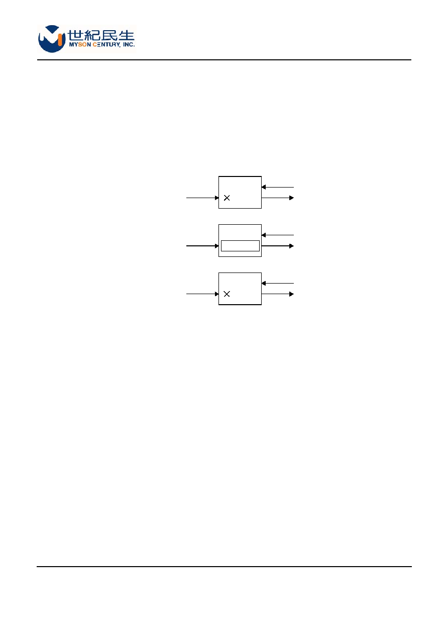
Flow Control
Flow control is used for adjusting transmission in full duplex mode. The PAUSE packet is used to request for
stopping/continuing transmission. The MTD503 will assert PAUSE to the linking station while the receiving frame
buffer of that port is near full. The pause time field in the PAUSE frame is "0xffff". If the frame buffer does not
remain at buffer-full before the pause timer times out, the MTD503 will assert a PAUSE with zero PAUSE time to
inform the linking station to recover transmission.
The buffer-full threshold is adjustable. If the buffer's free space becomes lower than the threshold, the MTD503
becomes ready to assert the PAUSE packet. Register 12, EEPROM.P0PSTH and EEPROM.P1PSTH, define the
threshold of Port0 and Port1, respectively.
Programmable Maximum Packet Length
The maximum packet size of a normal packet is defined in Register 12, EEPROMReg.MAXNORM. The packet is
not valid if its length is longer than that. Register 12, EEPROMReg.MAXVLAN, and Register 12,
EEPROMReg.MAXJB, define the maximum packet of VLAN packet and jumbo packet, respectively. They are
available only when Register 10, JumperReg0.VLANEN or JumperReg0.JBEN is set to "1".
Link Pass Through Mode
In this mode, the MTD503 forces to disable its copper PHY while the ifiber PHY is in link-down state. Only when
CONFIDENTIAL

page 11 of 37
MTD503
Preliminary
the fiber PHY becomes link-up, the coppy PHY is allowed to start the linking procedure. Set Register 11,
JumperReg1.LNKTHRGHEN to "1" to enable this mode.
Cut Through Mode
In this mode, the MTD503 transers packets without store-and-forward if both ports are at 100M and full duplex.
The latency for packets travelling through the MTD503 is reduced compared to that in the store-and-foward
mode.
Note that the SA learning, packet filtering, CRC check, and length check are not performed in this mode. To
enable this mode, set Register 11, JumperReg1.CUTTHRGHEN, to "1".
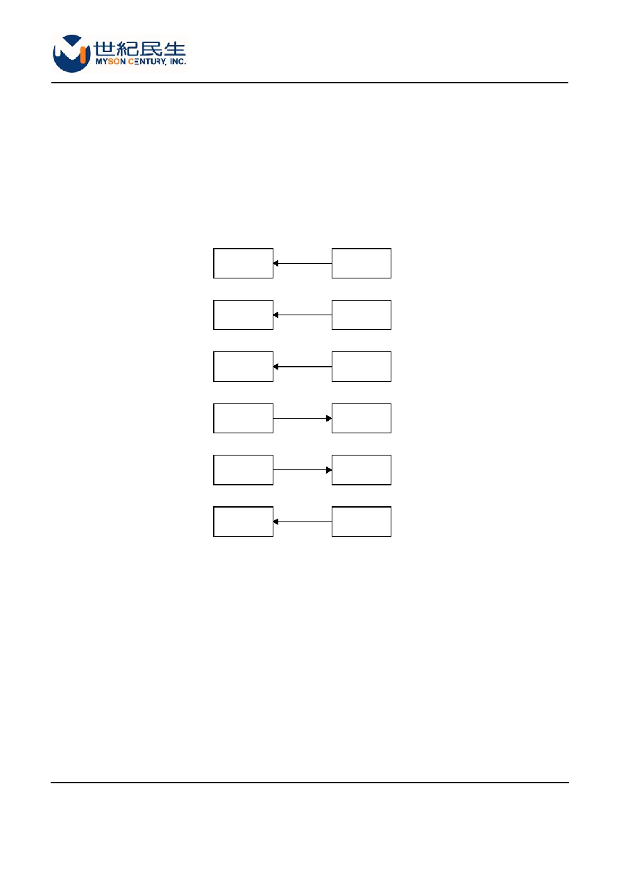
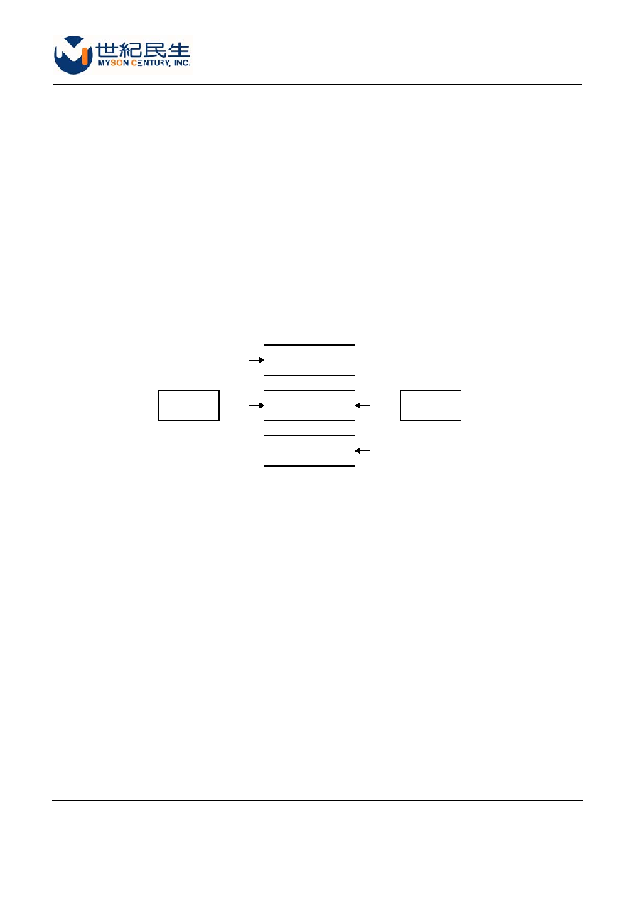
Look Back Mode
The MTD503 provides 4 types of loop back, and Register 15, SwCtrlReg, defines them. One of the four modes is
available each time.
i) Fiber Loop Back
Set LPBKPT to "00" to select this mode. The packet travel path is: fiber PHY line in --> fiber PHY MII RX out -->
fiber PHY MII TX in --> fiber PHY line out.
ii) Copper Loop Back
Set LPBKPT to "11" to select this mode. The packet travel path is : copper PHY line in --> copper PHY MII RX out
--> copper PHY MII TX in --> copper PHY line out.
iii) Port0 MAC Loop Back
Set LPBKPT to "10" to select this mode. The packet travel path is: fiber PHY line in --> fiber PHY MII RX out -->
P0 MAC MII RX in --> P1 MAC MII TX out --> P1 MAC MII RX in --> P0 MAC MII TX out --> fiber PHY MII TX in -
-> fiber PHY line out.
iv) Port1 MAC Loop Back
Set LPBKPT to "01" to select this mode. The packet travel path is : copper PHY line in --> copper PHY MII RX out
--> P1 MAC MII RX in --> P0 MAC MII TX out --> P0 MAC MII RX in --> P1 MAC MII TX out --> copper PHY MII
TX in --> copper PHY line out.
P0
P1
Port1 MAC Loop Back
Fiber Loop Back
Port0 MAC Loop Back
Copper Loop Back
PHY0
PHY1
SW
P0
P1
PHY0
PHY1
SW
CONFIDENTIAL

page 12 of 37
MTD503
Preliminary
OAM PACKET RECEIVING AND TRANSMISSION
OAM packet is used for exchanging the status between two endpoints of a fiber line. OAM packet is not in an
Ethernet packet format. The MTD503 supports OAM packet of length 4 to 16 bytes. The OAM TX/RX module
locates betwen MAC and fiber PHY. It is in charge of OAM packet transmission and receiving. In transmission, it
inserts OAM packet in MII traffic, with leaving 96 bit-time gap between packet. In receiving, the OAM TX/RX
module can detect the OAM packet from MII traffic. The MAC layer throws aways OAM packet since its length is
less than the minimum packet length (64 bytes). Following sections describes the receiving and transmission of
OAM packet.
Receive an OAM Packet
A uP or CPU can read back the OAM packet from the MTD503 through SMI (Serial Management Interface).
Before reading, uP has to set the maximum OAM packet length (Register 7: InPktCtrlReg1.MAXLENG and
InPktCtrlReg1.LENGFILTER), OAM pattern register (Register 8: PtnReg0, Register 9: PtnReg1) and the
associated mask registers (Register 8: MskReg0, Register9: MzkReg1). For any packet longer than the
maximum OAM packet length, the OAM TX/RX mode will ignore it. The pattern register defines the header
pattern of the OAM packet and the mask register defines the bit for checking. For a coming packet, the OAM TX/
RX module compares the first 32 bits of the packet with PtnReg0 and PtnReg1.It accepts that packet as an OAM
packet only if all the checked bits match patterns.
Once an OAM packet is successfully accepted and placed in the OAM buffer, the MTD503 can assert interrupt if
IntEnReg.NOTEMPTEN is turned on. Once the uP detects the interrupt, it needs to read the Register 3
PktIntStsReg first. At this time, uP will find that PktIntSts.NOTEMPT is "1". It means that the OAM receive buffer
is not empty. Before reading the OAM packet length and its CRC status, uP has to disable that interrupt source
(set IntEnReg.NOTEMPTEN to "0") in its interrupt routing. Next, uP checks the CRC status and reads the OAM
packet length. If uP decides to read the OAM packet, InPktCtrlReg.PTNMSKSEL needs to be set to "00" for
choosing INPKTDATA0, INPKTDATA1, INPKTDATA2 and INPKTDATA3. OAM packet data can be read back
from Register 8 to Register f. After getting the OAM packet, uP needs to move to the next OAM packet, clear the
interrupt source, and then turn on IntEnReg.NOTEMPTEN.
MTD503
uP
MTD503
uP
MTD503
uP
MTD503
uP
MTD503
uP
MTD503
uP
MTD503
uP
MTD503
uP
MTD503
uP
(1) Interrupt
(2) Read sts
(3) NOTEMPTY == 1
(4) Write
NOTEMPTEN <= 0
(5) Read
PKTLENG, CRCSTS
(6) Write
PTNMSKSEL <= 00
(7) Read
PktData
(8) Write
LOADNEXT <= 1
(10) Write
NOTEMPTEN <= 1
(9) Write
NOTEMPTY <= 1
CONFIDENTIAL
page 13 of 37
MTD503
Preliminary
Transmit an OAM Packet
To transmit an OAM packet, uP writes data to Register 8 to Register f. InPktCtrlReg.PTNMSKSEL needs to be
set to "00" for choosing OUTPKTDATA0, OUTPKTDATA1, OUTPKTDATA2 and OUTPKTDATA3. Next, set
Register 5 for OAM out packet control. OutPktCtrlReg.TXCNT is the number of bytes for transmitting. If set
OutPktCtrlReg.GENCRC = 1, the last byte of transmission will be replaced by an 8-bit CRC. If set
OutPktCtrlReg.FORCEOUT = 1, the OAM TX module stops the MII traffic from MAC and sends the OAM packet
directly. Once the OAM packet and output control setting are ready, uP set OutPktCtrlReg.OUTREQ = 1 to start
OAM transmission. When transmission ends, PktIntStsReg.OUTCMPLT becomes "1" and that will induce an
interrupt to inform the uP. The uP writes PktIntStsReg.OUTCMPLT = 1 to clear this interrupt.
MTD503
uP
MTD503
uP
MTD503
uP
MTD503
uP
MTD503
uP
MTD503
uP
(1) Write PktData
(2) Write TXCNT/FORCEOUT/GENCRC
(3) Write OUTREG <= 1
(4) Interrupt
(5) Read sts
(6) OUTCMPLT == 1
(7) Write OUTCMPLT <= 1
CONFIDENTIAL

page 14 of 37
MTD503
Preliminary
OPTIONAL SETTING
The MTD503 provides serveral functional options. Three ways to set these optional settings: by reset setting
pins, EEPROM, or through SMI. Following describes these functional options.
JBEN
Enable Jumbo frame function. Set 1 to enable and 0 to disable. The default value is 0. In this mode, the MAC
compares the type field of the received packet with jumbo tag before checking the packet length. It is with a
jumbo frame tag (0X8870), the MAC allows the frame size to be as large as MAXJB. The packet filtering and
CRC check are also performed. If this mode is not enabled, the MAC considers the packet with jumbo tag as a
normal packet and MAXNORM is used as the packet length limitation.
BROADCAS_0, BROADCAS_1
Enable broadcast function. When this function is enabled, the filtering and learning functions at that port are
disabled. Every packet is considered as a broadcast packet and must be forwarded to the next port if the packet
length and CRC are valid. This function is also available for jumbo frames.
LENGDIS_0, LENGDIS_1
Disable checking packet length. When this mode is enabled, the packet length is not limited by MAXNORM,
MAXJB, or MAXVLAN. The packet length can be as long as 9KB, including DA, SA, length/type, data, and CRC
fields. If a packet were longer than 9KB, it would be dropped. CRC check is still performed in this mode unless
CRC check is disabled by setting CRCDIS to 1.
FCDIS_0, FCDIS_1
Flow control option pins for Port0 and Port1, respectively. When set to "1", the MTD503 will not assert PAUSE
frame while frame buffer is near full. For the received PAUSE, the MTD503 will not stop transmission. The
PAUSE frame could be dropped or forwarded to another port, dependent on the setting of PAUSEOPT. Flow
control option is only available in full duplex mode.
PMBLOPT
Reserved.
IPGOPT
Reserved.
CRCDIS_0, CRCDIS_1
Disable CRC check for Port0 and Port1, respectively. When set to "1", the MAC does not check CRC field of the
received packet. When set to "0", the MAC checks CRC field and drops packet with CRC error.
VLANEN
VLAN enable. Set 1 to enable and 0 to disable. While this function is enabled, the MAC can recognize the VLAN
packet. The VLAN packet and 802.3 packets are similar. The preamble, DS, and SA follow 802.3 packet format.
Next to that, 2 bytes are for length/type field. The data payload can vary from 42 bytes to 1500 bytes. The last 4
bytes are CRC. The longest VLAN packet is defined in 802.3 is 1522 bytes. Extended the maximum VLAN
packet length is allowed in the MTD503. In this mode, MAXVLAN is used to examine the VLAN packet length. If
not in this mode, the VLAN packet is considered as a normal packet and the MAC will drop the VLAN packet that
is longer than MAXNORM.
The filtering, learning and aging functions work in this mode. If both VLAN and jumbo mode are enabled, the
MAC checks VLAN packets using MAXVLAN, and checks jumbo packet using MAXJB.
BKPRSDIS
CONFIDENTIAL
page 15 of 37
MTD503
Preliminary
Disable backpressure for both ports. The backpressure is for preventing buffer full in half duplex mode. While
buffer is near full and if this function is enabled, the MAC asserts JAM pattern to collide the coming packet. If this
mode is disabled, the MAC never asserts JAM patterns. This mode is available for half duplex mode only.
PAUSEOPT
PAUSE frame option, available only when flow control is disabled. Set 0 for termination mode and 1 for
transparent mode. In termination mode, the received PAUSE is dropped, that is, it is not forwarded to another
port. In transparent mode, the PAUSE frame is forwarded to another port, like forwarding a normal packet. If the
other port is in half duplex mode, the PAUSE frame is dropped.
TXCRCDIS
Disable TX CRC check. When enabled the CRC of TX frames are checked. Once the TX frame contains CRC
error, the read/write pointers of the frame buffer on that port are moved to the default position.
LNKTHRGHEN
Link pass through option. When enabled, the fiber PHY link-down event will force the copper PHY to be linked
down. When disabled, the copper PHY and fiber PHY start the link procedure individually.
CUTTHRGHEN
Enable cut through mode. In cut through mode, the fiber port and copper port are connected through a small
FIFO directly. Available only when both ports are at 100M and full dupled.
CLKOP
Clock output frequency option. This clock is for external uP or CPU. 1: the clock frequency is 12.5MHz; 0:
6.25HMz. The clock may is available after EEPROM loading finishes.
(1) Termination mode
PAUSE
Full/Half
(2) Transparent mode - full to full
PAUSE
Full
(3) Transparent mode - full to half
PAUSE
Half
Frame buffer
CONFIDENTIAL
page 16 of 37
MTD503
Preliminary
BLOCK CONFIGURATIONS
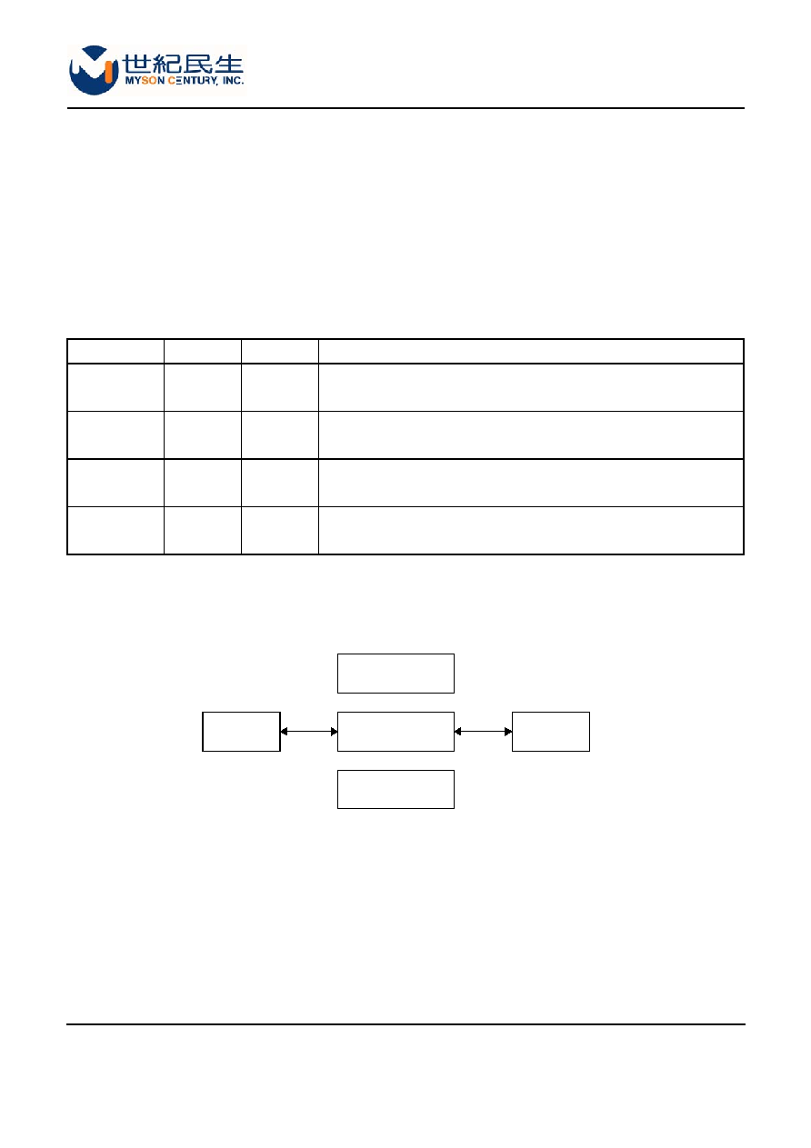
The MTD503 provides 4 configurations: embedded mode, external mode, SW-FX mode, and SW-TX mode.
Embedded Mode: two internal PHYs are active. Port0 is for 100Base-FX and Port1 is for 100Base-TX or
10Base-TX.
External mode: both internal PHYs are disabled. The MII0 and MII1 connect with SW engine.
SW-FX mode: two internal PHYs are activated but the MII between SW Port0 and FX PHY is separated. MII0
and MII1 connect with SW Port0 and FX PHY, respectively.
SW-TX mode: two internal PHYs are activated but the MII between SW Port1 and TX PHY is separated. MII1
and MII0 connect with SW Port1 and TX PHY, respectively.
Use PHYSEL0 and PHYSEL1 to select one of the configurations.
Embedded Mode
In this mode, SW Port0 connects with fiber PHY and SW Port1 connects with copper PHY. the Port0 MII and
Port1 MII are not used in this mode. The pad in/out directions follow that in the external mode, that is, only TXD
and TXEN are output. The OPTSPD and OPTFULL are not used in this mode. In this mode, the far end fault
indication pattern follows the 802.3 standard. Once fiber PHY detects LINK DOWN, it sends FEFI (84 ONEs and
1 ZERO) three times. In case fiber PHY received a FEFI, the event is recorded in fiber PHY's MII register.
Mode
PHYSEL0
PHYSEL1
Description
Embedded
Mode
0
0
Fiber PHY connects with SW Port0.
Copper PHY connects with SW Port1.
MII0 and MII1 are not used.
SW-TX mode
0
1
Fiber PHY connects with SW Port0.
Copper PHY connects with MII0.
SW Port1 connects with MII1.
SW-FX mode
1
0
Fiber PHY connects with MII1.
Copper PHY connects with SW Port1.
SW Port0 connects with MII0.
External mode
1
1
Internal PHY is not used.
SW Port0 connects with MII0.
SW Port1 connects with MII1.
Port0 MII
P0
P1
Copper PHY
Fiber PHY
Port1 MII
SW
CONFIDENTIAL

page 17 of 37
MTD503
Preliminary
SW-TX Mode
In this mode, the TX PHY and SW core are separated. SW Port1 connects with Port1 MII, and copper PHY
connects with Port0 MII. SW Port0 and fiber PHY are connected together. The in/out of Port1 MII pins have the
same directions as in the external mode. The Port0 MII works for copper PHY. However, the input and output
directions are different from that in the external mode.
- Copper PHY's RXD, RXDV, the output, go out through Port0 MII TXD and TXEN.
- Copper PHY's TXD and TXEN, the intputs, are connected with Port0 MII RXD and RXDV pins.
- Copper PHY's CRS, RXER, COL, TXC, RXC, are output. Use the same naming pins in Port0 MII, but
change the direction to output.
- SPD0 and FULL0 are for copper PHY's setting.
- SPD1 and FULL1 are for SW Port1's setting.
- OPTSPD and OPTFULL are not used.
SW-FX Mode
This mode is similar to SW-TX mode. In this mode, the FX PHY and SW core are separated. SW Port0 connects
with Port0 MII, and fiber PHY connects with MII0. SW Port1 and copper PHY are connected together. The in/out
of Port0 MII pins have the same directions as that in the external mode. The Port1 MII works for fiber PHY.
However, the intput and output directions are different from that in the external mode:
- Fiber PHY's RXD, RXDV, the outputs, go out through Port1 MII TXD and TXEN.
- Fiber PHY's TXD and TXEN, the inputs, are connected with Port1 MII RXD and RXDV pins.
Port0 MII
P0
P1
Copper PHY
Fiber PHY
Port1 MII
SW
Port0 MII
P0
P1
Copper PHY
Fiber PHY
Port1 MII
SW
CONFIDENTIAL
page 18 of 37
MTD503
Preliminary
- Fiber PHY's CRS, RXER, COL, TXC, RXC are output. Use the same naming pins in Port1 MII, but set the
direction to output.
- SPD0 and FULL0 are for SW Port0's setting.
- SPD1 and FULL1 are for fiber PHY's setting.
- OPTSPD and OPTFULL are for copper PHY's setting.
In this mode, some pins of Port1 MII are used for FEF control.
- COL1 indicates the receiving of an FEFI.
- SPD1 is used to select the FEFI pattern, either using default or coming from MII.
- FULL1 is used as TXD[4]. Associate with RXD0_1, RXD1_1, RXD2_1, and RXD3_1 to form the customer's
FEFI pattern.
External Mode
In this mode, both PHY are not used. SW Port0 and Port1 connect with Port0 MII and Port1 MII, respectively.
Only TXD and TXEN are outputs. Reset pins are input. OPTSPD and OPTFULL are not used.
Port0 MII
P0
P1
Copper PHY
Fiber PHY
Port1 MII
SW
CONFIDENTIAL

page 19 of 37
MTD503
Preliminary
REGISTER DESCRIPTION
DEVICE ID
Copper PHY, fiber PHY, and switch engine are three embedded devices in the MTD503.
Their default device ID is:
REGISTERS OF FIBER PHY
Register 0h: FxCtrlReg
Register 1h: FxStsReg
Device
Device ID[4]
Device ID[3]
Device ID[2]
Device ID[1]
Device ID[0]
Fiber PHY
0
1
0
0
1
Copper PHY
0
1
0
1
0
SW engine
0
1
0
1
1
Bit
Name
R/W
Default
Description
15
RST
R/W
0
Soft reset. 1: reset; 0: no action. Self-clear.
14
LBK100
R/W
0
Loop back for 100TX PHY. 1: enabled; 0: disable.
13
-
R/W
1
Reserved.
12
-
R/W
0
Reserved.
11
-
R/W
0
Reserved.
10
-
R/W
0
Reserved.
9
-
R/W
0
Reserved.
8
-
R/W
1
Reserved.
7
-
R/W
0
Reserved.
6
-
R/W
0
Reserved.
5:0
-
R/W
000000
Reserved.
Bit
Name
R/W
Default
Description
15
-
R
0
Reserved.
14:11
-
R
1111
Reserved.
10:5
-
R
000000
Reserved.
4
RFS
R
0
Remote fault status. 1: remoted fault received; 0: remote fault not
received. Auto update after reading this register.
3
-
R
1
Reserved.
2
LNK
R
0
Link status: 1: link up; 0: experienced link down. Auto update after
reading this register.
1
-
R
0
Reserved.
0
EXT
R
1
Extended capability.
CONFIDENTIAL

page 20 of 37
MTD503
Preliminary
Register 2h: FxOuiReg1
Register 3h: FxOuiReg2
Register 4h-10h: Reserved
Register 11h: FxProConfReg
Register 12h: Reserved
Register 13h: FxProStsReg
Register 1ah-1fh: Reserved
Bit
Name
R/W
Default
Description
15:0
OUI
R
0302
OUI 3rd bit to 18th bit.
Bit
Name
R/W
Default
Description
15:10
OUI
R
110100
OUI 19th bit to 24th bit.
9:4
MD
R
000000
Model number.
3:0
RV
R
0000
Revision number.
Bit
Name
R/W
Default
Description
15
-
R/W
1
Reserved.
14:7
-
R/W
00000000
Reserved.
6:5
-
R/W
11
Reserved.
4
TXOFF
R/W
0
Turn off 100BaseTx output. 1: turn off; 0: do not turn off.
3:0
-
R/W
000
Reserved.
Bit
Name
R/W
Default
Description
15:11
-
R
00000
Reserved.
10
-
R/W
1
Reserved.
9
-
R
0
Reserved.
8
FEFE
R/W
0
Enable far end fault function. 1: enable; 0: disable.
7
DPLX
R
0
Reflect current duplex status. 1: full duplex; 0: half duplex.
6
SPD
R
0
Reflect current speed status. 1: 100Mbps; 0: not 100Mbps.
5
CONN
R
0
Reflect current link status. 1: link up; 0: link down.
4:0
R
01001
Reserved.
CONFIDENTIAL

page 21 of 37
MTD503
Preliminary
REGISTERS OF COPPER PHY
Register 0h: TpCtrlReg
Register 1h: TpStsReg
Register 2h: TpOuiReg1
Bit
Name
R/W
Default
Description
15
RST
R/W
0
Soft reset. 1: reset; 0: no action. Self-clear.
14
LBK
R/W
0
Loop back mode. 1: enable; 0: disable.
13
SPD
R/W
1
Speed mode. 1: 100Mbps; 0: 10Mbps.
12
ANEN
R/W
1
Auto negotiatioin. 1: enable; 0: disable.
11
-
R/W
0
Reserved.
10
-
R/W
0
Reserved.
9
REAN
R/W
0
Re-start auto negotiation. 1: restart; 0: do not restart.
8
DUPLEX
R/W
0
Duplex mode. 1: full; 0: half.
7
-
R/W
0
Reserved.
6
-
R/W
0
Reserved.
5:0
-
R/W
000000
Reserved.
Bit
Name
R/W
Default
Description
15
-
R
0
Reserved.
14
TXFD
R
1
Capable of 100Base-TX full duplex. 1: capable; 0: not capable.
13
TDHD
R
1
Capable of 100Base-TX half duplex. 1: capable; 0: not capable.
12
TPFD
R
1
Capable of 10Base-T full duplex. 1: capable; 0: not capable.
11
TPHD
R
1
Capable of 10Base-T half duplex. 1: capable; 0: not capable.
10:7
-
R
0000
Reserved.
6
-
R
1
Reserved.
5
ANDONE
R
0
Auto negotiation status. 1: complete; 0: not complete.
4
-
R
0
Reserved.
3
ANCAP
R
1
Auto negotiation capability. Always 1.
2
LNK
R
0
Link status. 1: link up; 0: link down.
1
JAB
R
0
Jabber detected. 1: detected; 0: not detected.
0
-
R
1
Reserved.
Bit
Name
R/W
Default
Description
15:0
OUI
R
0302
OUI 3rd bit to 18th bit.
CONFIDENTIAL

page 22 of 37
MTD503
Preliminary
Register 3h: TpOuiReg2
Register 4h: TpAnAdvReg
Register 5h: TpAnLnkPnrReg
Register 6h-9h: Reserved
Bit
Name
R/W
Default
Description
15:10
OUI
R
110100
OUI 19th bit to 24th bit.
9:4
MD
R
000000
Model number.
3:0
RV
R
0000
Revision number.
Bit
Name
R/W
Default
Description
15
NP
R
0
Next page indication. 1: next page enable; 0: next page disable.
14
ACK
R
0
Received link code word acknowledgement.
1: acknowledged; 0: not acknowledge.
13
-
R
0
Reserved.
12:11
-
R/W
00
Reserved.
10
-
R/W
0
Reserved.
9
-
R
0
Reserved.
8
TXFD
R
1
100Base-TX full duplex ability. 1: capable; 0: not capable.
7
TXHD
R
1
100Base-TX half duplex ability. 1: capable; 0: not capable.
6
TPFD
R
1
10Base-T full duplex ability. 1: capable; 0: not capable.
5
TPHD
R
1
10Base-T half duplex ability. 1: capable; 0: not capable.
4:0
-
R
00001
Reserved.
Bit
Name
R/W
Default
Description
15
NP
R
0
Next page indication. 1: next page enable; 0: next page disable.
14
ACK
R
0
Received link code word acknowledgement.
1: acknowledged; 0: not acknowledge.
13
-
R
0
Reserved.
12:11
-
R
00
Reserved.
10
-
R
0
Reserved.
9
-
R
0
Reserved.
8
TXFD
R
0
100Base-TX full duplex ability. 1: capable; 0: not capable.
7
TXHD
R
0
100Base-TX half duplex ability. 1: capable; 0: not capable.
6
TPFD
R
0
10Base-T full duplex ability. 1: capable; 0: not capable.
5
TPHD
R
0
10Base-T half duplex ability. 1: capable; 0: not capable.
4:0
-
R
00001
Reserved.
CONFIDENTIAL
page 23 of 37
MTD503
Preliminary
Register 10h: TpProCtrlReg
Register 11h: Reserved
Register 12h: TpProStsReg
Register 13h-1fh: Reserved
Bit
Name
R/W
Default
Description
15:11
-
R/W
00000
Reserved.
10:9
-
R/W
11
Reserved.
8:7
-
R/W
00
Reserved.
6
XFSEL
R/W
0
Transmit transformer ratio select. 1: [1.25:1]; 0: [1:1].
5
POLDIS
R/W
0
Auto polarity detection/correction function. 1: disable; 0: enable.
4:3
-
R/W
00
Reserved.
2
JABDIS
R/W
0
Jabber function. 1: disable; 0: enable.
1
SCRMEN
R/W
1
Scramble function. 1: enable; 0: disable.
0
-
R/W
0
Reserved.
Bit
Name
R/W
Default
Description
15:12
-
R
000
Reserved.
11
DUPLEX
R
0
Duplex after link established. 1: link up and in full duplex; 0: link
down or link up in half duplex.
10
SPEED
R
0
Link speed. 1: 100Base-TX; 0: 10Base-T.
9:5
-
R
00000
Reserved.
4:0
-
R
01010
CONFIDENTIAL

page 24 of 37
MTD503
Preliminary
REGISTERS OF SWITCH
The device ID after power on is 000011. After completing reset, the first three MSB of the device ID are loaded
from EEPROM.
Register 0h - Register fh: OAM Packet Data, Control, Status Registers
The OAM packet is a small packet with length from 4 to 16 bytes. It is not the 802.3 MAC packet format.
Customers can specify it. The IPG is 96-bit time. TS-1000 packet is an OAM packet with 12-byte length. The
CRCSTS is the 8-bit CRC result.
Registers 0h-2h: Reserved.
Register 3h: PktIntStsReg
Interrupt status register.
Register 4h: IntEnReg
Interrupt enable/disable control.
Register 5h: OutPktCtrlReg
Bit
Name
R/W
Default
Description
15
OUTBUSY
R
0
1: busy at sending OAM packet; 0: idle. Will not cause interrupt.
14
OUTCMPLT
R/W
0
1: complete sending OAM packet. Write 1 to clear.
13
INBUFULL
R/W
0
1: in-packet buffer full; 0: not full. Write 1 to clear.
12
NOTEMPT
R/W
0
1: at least one packet has come into in-packet buffer. Write 1 to
clear.
11
OVERFLOW
R/W
0
1: new OAM event when buffer already full. Write 1 to clear.
10:0
-
R/W
0
Reserved.
Bit
Name
R/W
Default
Description
15
-
R/W
0
Reserved.
14
OUTCMPLTEN
R/W
0
1: enable interrupt; 0: disable.
13
INBUFULLEN
R/W
0
1: enable interrupt; 0: disable.
12
NOTEMPTEN
R/W
0
1: enable interrupt; 0: disable.
11
OVERFLOWEN
R/W
0
1: enable interrupt; 0: disable.
10:0
-
R/W
0
Reserved.
Bit
Name
R/W
Default
Description
15
OUTREQ
W
1: request for sending OAM packet; 0: no action. Effective only
when OUTBUSY == 0. Request cleared automatically after send-
ing out packet.
14
GENCRC
R/W
1: calculate CRC for the data from OUTPKTDATA1 to last byte,
and then append it to the last byte of the out packet.
0: do not append CRC.
CONFIDENTIAL

page 25 of 37
MTD503
Preliminary
Register 6h: InPktCtrlReg0
Register 8h - Register fH: OAM Packet Data Registers
Register 8h: PktData0_1/PtnReg0/MskReg0
13
FORCEOUT
R/W
0
1: force to send out OAM packet. The normal packet might be vio-
lated;
0: insert OAm packet without violating the normal packet.
12:8
TXCNT
R/W
`d12
Byte count of transmit packet. Only 4 to 16 are allowed.
7:1
-
R/W
0
Reserved.
0
OUTBUFRST
W
Reset OAM out-packet buffer. One click. Automatically cleared.
Bit
Name
R/W
Default
Description
15:13
PKTCNT
R
00
Number of packets in buffer.
12:8
PKTLENG
R
0
Packet length of the OAM buffer. Updated after loading whole
OAM packet into buffer.
7:6
PTNMAKSEL
R/W
00
Packet data, pattern register, mask register selection for Register8
and Register 9.
00: PktData; 01: PtnReg; 10: MskReg; 11: reserved.
5
LOADNEXT
W
1: load next OAm packet; 0: no action.
Request cleared automatically after loading completes.
4
CRCSTS
R
0
CRC status of current OAM packet in buffer.
1: CRC error; 0: CRC OK.
Updated after loading OAM packet.
3:0
-
R/W
0
Reserved.
Bit
Name
R/W
Default
Description
(1) InPktCtrlReg.PTNMSKSEL == 00
15:8
INPKTDATA0
R
0
0th byte of the OAM packet.
7:0
INPKTDATA1
R
0
1st byte of the OAM packet.
15:8
OUTPKTDATA0
W
0th byte of the OAM packet.
7:0
OUTPKTDATA1
W
1st byte of the OAM packet.
(2) InPktCtrlReg.PTNMSKSEL == 01
15:8
PATTERN0
R/W
0
0th byte pattern for OAM packet filtering.
7:0
PATTERN1
R/W
0
1st byte pattern for OAM packet filtering.
(3) InPktCtrlReg.PTNMSKSEL == 10
15:8
MASK0
R/W
0
0th mask byte. 1: mask, not check that bit. 0: unmask.
7:0
MASK1
R/W
0
1st mask byte. 1: mask, not check that bit. 0: unmask.
Bit
Name
R/W
Default
Description
CONFIDENTIAL

page 26 of 37
MTD503
Preliminary
Register 9h: PktData2_3/PtnReg1/MskReg1
Register ah: PktData4_5
Register bh: PktData6_7
Bit
Name
R/W
Default
Description
(1) InPktCtrlReg.PTNMSKSEL == 00
15:8
INPKTDATA2
R
0
2nd byte of the OAM packet.
7:0
INPKTDATA3
R
0
3rd byte of the OAM packet.
15:8
OUTPKTDATA2
W
2nd byte of the OAM packet.
7:0
OUTPKTDATA3
W
3rd byte of the OAM packet.
(2) InPktCtrlReg.PTNMSKSEL == 01
15:8
PATTERN2
R/W
0
2nd byte pattern for OAM packet filtering.
7:0
PATTERN3
R/W
0
3rd byte pattern for OAM packet filtering.
(3) InPktCtrlReg.PTNMSKSEL == 10
15:8
MASK2
R/W
0
2nd mask byte. 1: mask, not check that bit. 0: unmask.
7:0
MASK3
R/W
0
3rd mask byte. 1: mask, not check that bit. 0: unmask.
Bit
Name
R/W
Default
Description
15:8
INPKTDATA4
R
0
4th byte of the OAM packet.
7:0
INPKTDATA5
R
0
5st byte of the OAM packet.
15:8
OUTPKTDATA4
W
4th byte of the OAM packet.
7:0
OUTPKTDATA5
W
5th byte of the OAM packet.
Bit
Name
R/W
Default
Description
15:8
INPKTDATA6
R
0
6th byte of the OAM packet.
7:0
INPKTDATA7
R
0
7th byte of the OAM packet.
15:8
OUTPKTDATA6
W
6th byte of the OAM packet.
7:0
OUTPKTDATA7
W
7th byte of the OAM packet.
CONFIDENTIAL
page 27 of 37
MTD503
Preliminary
Register ch: PktData8_9
Register dh: PktData10_11
Register eh: PktData12_13
Register fh: PktData14_15
Register 10h: JumperReg0
This register keeps all of the jumper setting value. They are loaded at the end of reset edge and able to be
Bit
Name
R/W
Default
Description
15:8
INPKTDATA8
R
0
8th byte of the OAM packet.
7:0
INPKTDATA9
R
0
9th byte of the OAM packet.
15:8
OUTPKTDATA8
W
8th byte of the OAM packet.
7:0
OUTPKTDATA9
W
9th byte of the OAM packet.
Bit
Name
R/W
Default
Description
15:8
INPKTDATA10
R
0
10th byte of the OAM packet.
7:0
INPKTDATA11
R
0
11th byte of the OAM packet.
15:8
OUTPKTDATA10
W
10th byte of the OAM packet.
7:0
OUTPKTDATA11
W
11th byte of the OAM packet.
Bit
Name
R/W
Default
Description
15:8
INPKTDATA12
R
0
12th byte of the OAM packet.
7:0
INPKTDATA13
R
0
13th byte of the OAM packet.
15:8
OUTPKTDATA12
W
12th byte of the OAM packet.
7:0
OUTPKTDATA13
W
13th byte of the OAM packet.
Bit
Name
R/W
Default
Description
15:8
INPKTDATA14
R
0
14th byte of the OAM packet.
7:0
INPKTDATA15
R
0
15th byte of the OAM packet.
15:8
OUTPKTDATA14
W
14th byte of the OAM packet.
7:0
OUTPKTDATA15
W
15th byte of the OAM packet.
CONFIDENTIAL

page 28 of 37
MTD503
Preliminary
modified via this register.
Register 11h: JumperReg1
Bit
Name
R/W
Default
Description
15
CRCDIS_1
R/W
0
1: disable Port1 CRC check; 0: enable Port1 CRC check.
14
CRCDIS_0
R/W
0
1: disable Port0 CRC check; 0: enable Port0 CRC check.
13
VLANEN
R/W
0
1: enable VLAN tag; 0: do not support.
12
BKPRSDIS
R/W
0
1: disable backpressure; 0: enable backpressure.
11
PAUSEOPT
R/W
0
1: transparency mode; 0: termination mode.
10
TXCRCDIS
R/W
0
1: disable TX CRC check and auto recovery; 0: enable.
9
Reserved
R/W
0
Reserved.
8
JBEN
R/W
0
1: enable jumbo mode; 0: disable.
7
FCDIS_1
R/W
0
1: disable Port1 flow control; 0: enable.
6
FCDIS_0
R/W
0
1: disable Port0 flow control; 0: enable.
5
IPGOPT
R/W
0
Reserved.
4
PMBLOPT
R/W
0
Reserved.
3
BROADCAS_1
R/W
0
1: disable Port1's packet filtering. 0: enable filtering.
2
BROADCAS_0
R/W
0
1: disable Port0's packet filtering. 0: enable filtering.
1
LENGDIS_1
R/W
0
1: do not check Port1's packet length; 0: check.
0
LENGDIS_0
R/W
0
1: do not check Port0's packet length; 0: check.
Bit
Name
R/W
Default
Description
15
LNKTHRGHEN
R/W
0
Link pass through option. 1: enable; 0: disable.
14
CUTTHRGHEN
R/W
0
Cut through option. 1: enable; 0: disable.
12
CLKOPT
R/W
0
Clock output option. 1: 12.5MHz; 0: 6.25MHz.
11
ID4
R/W
0
SW engine device ID[4].
10
ID3
R/W
1
SW engine device ID[3].
9
ID2
R/W
0
SW engine device ID[2].
8
FASTMODE
R/W
0
1: enable fast mode. Must be set to 0 in normal operation.
7:5
-
Reserved.
4
EPROMDONE
R
0
EEPROM loading complete. 1: complete; 0: not complete.
3:0
EPROMIDX
R/W
0
Index for EEPROMReg (Register 12).
0: reserved;
1: SA[15:0];
2: SA[31:16];
3: SA[47:23];
4: MAXNORM;
5: MAXVLAN;
6; MAXJB;
7: buffer threshold;
8-15: reserved.
CONFIDENTIAL

page 29 of 37
MTD503
Preliminary
Register 12h: EEPROMReg
This register defines SA, MAXNORM, MAXJB, and buffer threshold.
Register 13h: BufStsReg
Bit
Name
R/W
Default
Description
(1) JumperReg: EEPROMIDX == 0001
15:0
SA0
R/W
0
SA[15:0]
(2) JumperReg: EEPROMIDX == 0010
15:0
SA1
R/W
0
SA[31:16]
(3) JumperReg: EEPROMIDX == 0011
15:0
SA2
R/W
0
SA[47:32]
(4) JumperReg: EEPROMIDX == 0100
15:0
MAXNORM
R/W
`d1536
Maximum packet length of normal packet.
(5) JumperReg: EEPROMIDX == 0101
15:0
MAXVLAN
R/W
`d1536
Maximum packet length of VLAN packet.
(6) JumperReg: EEPROMIDX == 0110
15:0
MAXJB
R/W
`d9216
Maximum packet length of jumbo packet.
(7) JumperReg: EEPROMIDX == 0111
15:11
P1PSTH
R/W
00101
Port1 buffer pause threshold. Unit: 1K; default: 00101 (5K).
Recommended range: 00101 to 10110 (1K to 22K).
10:8
P1EMPTH
R/W
010
Port1 buffer empty threshold.
001: 1.5K; 010: 3K; 011: 4.5K; 100: 6K; 101: 7.5K; 110: 9K; 111:
10.5K.
Default: 101.
7:3
P0PSTH
R/W
00101
Port0 buffer pause threshold. Unit: 1K; default: 00101 (5K).
Recommended range: 00101 to 10110 (1K to 22K).
2:0
P0EMPTH
R/W
010
Port0 buffer empty threshold.
001: 1.5K; 010: 3K; 011: 4.5K; 100: 6K; 101: 7.5K; 110: 9K; 111:
10.5K.
Default: 101.
Bit
Name
R/W
Default
Description
15:8
-
Reserved.
7
P1BUFRST
W
Write 1 to reset Port1 buffer pointer. Write 0: no action.
6
P0BUFRST
W
Write 1 to reset Port0 buffer pointer. Write 0: no action.
CONFIDENTIAL

page 30 of 37
MTD503
Preliminary
Register 14h: Reserved
Register 15h: SwCtrlReg
5
P1BUFVIO
R/W
0
Read 1: Port1 buffer pointer violation occurs. Write 1 to clear the
status.
4
P1BUFVIO
R/W
0
Read 1: Port0 buffer pointer violation occurs. Write 1 to clear the
status.
3
P1BUFULL
R/W
0
Read 1: Port1 buffer full occurs. Write 1 to clear the status.
2
P1BUFEMP
R/W
1
Read 1: Port1 buffer becomes empty. Write 1 to clear the status.
1
P0BUFULL
R/W
0
Read 0: Port1 buffer full occurs. Write 1 to clear the status.
0
P0BUFEMP
R/W
1
Read 0: Port1 buffer becomes empty. Write 1 to clear the status.
Bit
Name
R/W
Default
Description
15:0
R/W
0
Reserved.
Bit
Name
R/W
Default
Description
15
LPBKEN
R/W
0
Loop back mode. 1: enable; 0: disable.
14:13
LPBKPT
R/W
0
Loop back point. 00: P0PHY; 01: P1MAC; 10: P0MAC; 11:
P1PHY. Available only when LPBKEN =1.
12
LPBKFILOAM
R/W
0
Filter OAM packet in loop back buffer.
1: enable filter function; 0: disable filter function.
11
P0FORCEFC
R/W
0
Force flow control on Port0. 1: enable; 0: disable.
10
P1FORCEFC
R/W
0
Force flow control on Port1. 1: enable; 0: disable.
9
P0FILOAM
R/W
0
Filter OAM packet in P0 to P1 cut through buffer.
1: enable filter function; 0: disable.
8
P1FILOAM
R/W
0
Filter OAm packet in P1 to P0 cut through buffer.
1: enable filter function; 0: disable.
7
P0LRNDIS
R/W
0
Disable Port0 learning.
1: disable Port0 learning; 0: enable Port0 learning.
6
P1LRNDIS
R/W
0
Disable Port1 learning.
1: disable Port1 learning; 0: enable Port1 learning.
5
Reserved.
4
P0TXENDIS
R/W
0
Port0 TXEN disable.
1: force switch P0TXEN = 0; 0: normal.
3
P0RXDVDIS
R/W
0
Port0 RXDV disable.
1: force switch P0RXDV = 0; 0: normal.
2
P1TXENDIS
R/W
0
Port1 TXEN disable.
1: force switch P1TXEN = 0; 0: normal.
1
P1RXDVDIS
R/W
0
Port1 RXDV disable.
1: force switch P1RXDV = 0; 0: normal.
0
SWRST
W
0
Reset switch. 1: reset; 0: no action. One click. Automatically
cleared.
Bit
Name
R/W
Default
Description
CONFIDENTIAL

page 31 of 37
MTD503
Preliminary
Register 16h: P0RdPtrReg
Register 17h: P0WrPtrReg
Register 18h: P1RdPtrReg
Register 19h: P1WrPtrReg
Register 1ah: AgingTime
Register 1bh: PktCntReg
Bit
Name
R/W
Default
Description
15:0
P0RDPTR
R
`h9800
Port0 frame buffer read pointer.
Bit
Name
R/W
Default
Description
15:0
P0WRPTR
R
`h3002
Port0 frame buffer write pointer.
Bit
Name
R/W
Default
Description
15:0
P1RDPTR
R
`h3000
Port1 frame buffer read pointer.
Bit
Name
R/W
Default
Description
15:0
P1WRPTR
R
`h9802
Port1 frame buffer write pointer.
Bit
Name
R/W
Default
Description
15:0
AGING
R/W
`d300
The initial age for each address entry.
Bit
Name
R/W
Default
Description
15
P1RXCLR
W
Write 1: clear Port1 RX packet count. Write 0: no action.
14
P1TXCLR
W
Write 1: clear Port1 TX packet count. Write 0: no action.
13
P0RXCLR
W
Write 1: clear Port0 RX packet count. Write 0: no action.
12
P0TXCLR
W
Write 1: clear Port0 TX packet count. Write 0: no action.
11:10
CNTSEL
W
Select the port counter for reading.
00: Port0RX; 01: Port0TX; 10: Port1RX; 11: Port1TX.
9:0
-
W
Reserved.
15:14
PORTIDX
R
0
Port count index.
00: Port0RX; 01: Port0TX; 10: Port1RX; 11: Port1TX.
13:0
PKTCNT
R
0
Packet count associated with PORTIDX.
CONFIDENTIAL

page 32 of 37
MTD503
Preliminary
Register 1ch: EEPROMUsrCtrlReg
Register 1dh: EEPROMUsrDataReg
Bit
Name
R/W
Default
Description
15:10
USRADDR
R/W
0
EEPROM user address.
9
USRLOAD
W
0
EEPROM user load.
1: request to load data from EEPROM;
0: no action.
8
USRDATARDY
R
0
EEPROM user data is loaded.
1: loading complete; 0: not ready.
7:0
-
Reserved.
Bit
Name
R/W
Default
Description
15:0
USRDATA
R
0
EEPROM user data.
CONFIDENTIAL

page 33 of 37
MTD503
Preliminary
EEPROM DESCRIPTIONS
The serial EEPROM is 93C46. Use 16-bit mode.
Bit
Name
Description
@ 0
15:8
Tag
Used as an identifier. Value: 8'h73.
7:0
LastAddr
Last address. Default: 8'h0c.
@ 1
15:0
SA[15:0]
SA[15:0]. Default: 0.
@ 2
15:0
SA[31:16]
SA[31:16]. Default: 0.
@ 3
15:0
SA[47:32]
SA[47:32]. Default: 0.
@ 4
15:14
Reserved.
13:0
MAXNORM
Maximum size of normal packet. Default: 1536.
@ 5
15:14
Reserved.
13:0
MAXVLAN
Maximum size of VLAN packet. Default: 1536.
@ 6
15:14
Reserved.
13:0
MAXJB
Maximum size of jumbo packet. Default: 9216.
@ 7
15:11
P1PSTH
Port1 buffer pause threshold. Unit: 1K; default: 00101 (5K). Legal range: 00001 to 10110
(1K to 22K). Must be greater than rejection threshold.
10:8
P1EMPTH
Port1 buffer empty threshold.
001: 1.5K; 010: 3K; 011: 4.5K; 100: 6K; 101: 7.5K; 110: 9K; 111: 10.5K.
Default: 101.
7:3
P0EMPTH
Port0 buffer pause threshold. Unit: 1K; default: 00101 (5K). Legal range: 00001 to 10110
(1K to 22K). Must be greater than rejection threshold.
2:0
P0EMPTH
Port0 buffer empty threshold.
001: 1.5K; 010: 3K; 011: 4.5K; 100: 6K; 101: 7.5K; 110: 9K; 111: 10.5K.
Default: 101.
CONFIDENTIAL

page 34 of 37
MTD503
Preliminary
@ 8
15:0
Reserved.
@ 9
15:0
Reserved.
@ a
15
CRCDIS_1
1: disable Port1 CRC check; 0: enable Port1 CRC check.
14
CRCDIS_0
1: disable Port0 CRC check; 0: enable Port0 CRC check.
13
VLANEN
1: enable VLAN tag; 0: do not support.
12
BKPRSDIS
1: disable backpressure; 0: enable backpressure.
11
PAUSEOPT
1: transparency mode; 0: termination mode.
10
TXCRCDIS
1: disable TX CRC check and auto recovery. 0: enable.
9
Reserved
Reserved.
8
JBEN
1: enable jumbo mode; 0: disable.
7
FCDIS_1
1: disable Port1 flow control; 0: enable.
6
FCDIS_0
1: disable Port0 flow control; 0: enable.
5
IPGOPT
1: enable short IPG; 0: disable.
4
PMBLOPT
1: enable short preamble; 0: disable.
3
BROADCAS_1
1: disable Port1's packet filtering; 0: enable filtering.
2
BROADCAS_0
1: disable Port0's packet filtering; 0: enable filtering.
1
LENGDIS_1
1: do not check Port1's packet length; 0: check.
0
LENGDIS_0
1: do not check Port0's packet length; 0: check.
@ b
15
LNKTHRGHEN
Link pass through option. 1: enable; 0: disable.
14
CUTTHRGHEN
Cut through option. 1: enable; 0: disable.
13
MDIXEN
MDIX option. 1: enable; 0: disable.
12
CLKOPT
Clock output option. 12.5MHz output; 0: 6.25MHz.
11
ID4
SW engine device ID [4].
10
ID3
SW engine device ID [3].
9
ID2
SW engine device ID [2].
8
FASTMODE
1: enable fast mode. Must be set to 0 in normal operation.
7:5
Reserved.
"1".
4
EPROMDONE
Must be set to "1".
3:0
EPROMIDX
Set to "0000".
Bit
Name
Description
CONFIDENTIAL

page 35 of 37
MTD503
Preliminary
PACKAGE
OUTLINE
103
128
102
65
64
39
38
1
D
D1
E
E1
e
B
SEE DETAIL "B"
SEATING PLANE
SEE DETAIL "A"
B
C
WITH PLATING
BASE METAL
L
L1
z
GAGE PLANE
y
Detail A
Detail B
A
A2
A1
CONFIDENTIAL

page 37 of 37
MTD503
Preliminary
Note 1.Dimension D1 & E1 do not include mold protrusion. But mold mismatch is included. Allowable protrusion is .25mm
.010" per side.
Note 2.Dimension B does not include dambar protrusion. Allowable dambar protrusion .08mm/.003". Total in excess of the
dimemsion at maximum material condition. Dambar cannot be located on the lower radius or the foot.
Note 3.Controlling dimension : Millimeter.
ORDERING INFORMATION
Standard Configuration
Symbol
Dimensions in Millimeters Dimensions
in
Inches
Min
Nom
Max
Min
Nom
Max
A
-
-
3.40
-
-
0.134
A1
0.25
-
-
0.010
-
-
A2
2.73
2.85
2.97
0.107
0.112
0.117
B
0.17
0.22
0.27
0.007
0.009
0.011
C
0.09
-
0.20
0.004
-
0.008
D
23.00
23.20
23.40
0.906
0.913
0.921
D1
19.90
20.00
20.10
0.783
0.787
0.791
E
17.00
17.20
17.40
0.669
0.667
0.685
E1
13.90
14.00
14.10
0.547
0.551
0.555
e
0.50BCS
0.020BCS
L
0.73
0.88
1.03
0.029
0.035
0.041
L1
1.60BCS
0.063BCS
y
-
-
0.10
-
-
0.004
z
0
∞
-
7
∞
0
∞
-
7
∞
Prefix
Part Type
Package Type
MTD
503
F:PQFP
CONFIDENTIAL