 | –≠–ª–µ–∫—Ç—Ä–æ–Ω–Ω—ã–π –∫–æ–º–ø–æ–Ω–µ–Ω—Ç: MTV038 | –°–∫–∞—á–∞—Ç—å:  PDF PDF  ZIP ZIP |

This datasheet contains new product information. Myson Technology reserves the rights to modify the product specification without notice.
No liability is assumed as a result of the use of this product. No rights under any patent accompany the sales of the product.
Revision 1.1
-1-
2001/8/21
MTV038
(Revision 1.1)
MYSON
TECHNOLOGY
FEATURES
GENERAL DESCRIPTION
BLOCK DIAGRAM
∑ Horizontal SYNC input up to 150 KHz.
∑ On-chip PLL circuitry or external pixel clock input up to
150 MHz.
∑ Software control for CRT/LCD applications.
∑ Programmable R,G,B input level for timing measurement
among HFLB, VFLB, RIN, GIN and BIN for auto sizing.
∑ Full screen self-test pattern generator.
∑ Programmable Hor. resolutions up to 1524 dots per line.
∑ Full-screen display consists of 15 (rows) by 30 (columns)
∑ Two font size 12x16 or 12x18 dot matrix per character.
∑ True totally 544 mask ROM fonts including 512 standard
fonts and 32 multi-color fonts.
∑ Character button boxes with programmable box length.
∑ Double character height and/or width control.
∑ Programmable positioning for display screen center.
∑ Character bordering, shadowing and blinking effect.
∑ Character (per row) and window intensity control.
∑ Row to row spacing control to avoid expansion distortion.
∑ 4 programmable windows with multi-level operation.
∑ Shadowing on windows with programmable shadow
width/height/color.
∑ Programmable adaptive approach to handle H, V sync
collision automatically by hardware.
∑ Software clears bit for full-screen erasing.
∑ Fade-in/fade-out or blending-in/blending-out effects.
∑ Compatible with SPI bus or I
2
C interface with slave
address 7AH/7BH (slave address is mask option).
∑ 16-pin or 20-pin PDIP/SOP package.
On-Screen Display Controller for CRT/LCD Monitor
MTV038 is designed for CRT/LCD monitor applications
to display built-in characters or fonts onto monitor screens.
The display operation occurs by transferring data and con-
trol information from the micro-controller to RAM through a
serial data interface. It can execute full-screen display
automatically, as well as specific functions such as charac-
ter background, bordering, shadowing, blinking, double
height and width, font by font color control, character but-
ton boxes, frame positioning, frame size control by charac-
ter height and row-to-row spacing, horizontal display
resolution, full-screen erasing, fade-in/fade-out effect, win-
dowing effect, shadowing on window and full-screen self-
test pattern generator.
MTV038 provides 544 fonts including 512 standard
fonts and 32 multi-color fonts and 2 font sizes, 12x16 or
12x18 for more efficacious applications. The full OSD
menu is formed by 15 rows x 30 columns, which can be
positioned anywhere on the monitor screen by changing
vertical or horizontal delay.
The auto sizing video measurement module measure
the timing relationship among HFLB, VFLB, and R, G, BIN
with 12-bit resolution at the speed related to the OSD pixel
clock. And the R, G, BIN input level can be programming
by software. MCU can get the measurement data, active
video, front porth and back porth, through I
2
C bus read/
write operation to keep the appropriate display size and
center.
SERIAL DATA
INTERFACE
ADDRESS BUS
ADMINISTRATOR
VERTICAL
DISPLAY
CONTROL
DISPLAY & ROW
CONTROL
REGISTERS
COLOUR
ENCODER
WINDOWS &
FRAME
CONTROL
WR
WG
WB
FBKGC
BLANK
LUMAR
LUMAG
LUMAB
BLINK
VCLKX
DATA
VERTD
HORD
CH
8
8
7
BSEN
SHADOW
OSDENB
HSP
VSP
HORIZONTAL
DISPLAY CONTROL
PHASE LOCK LOOP
8
DATA
LPN
CWS
VCLKS
5
DATA
CWS
CHS
8
LUMAR
LUMAG
LUMAB
BLINK
CRADDR
8
LUMA
BORDER
ARWDB
HDREN
VCLKX
HORD 8
CH
CHS
VERTD
7
8
LPN
NROW
VDREN
5
RCADDR
DADDR
FONTADDR
WINADDR
PWMADDR
5
9
9
5
5
ARWDB
HDREN
VDREN
NROW
DATA
ROW, COL
ACK
8
9
CHARACTER ROM
LUMINANCE &
BORDGER
GENERATOR
VDD
VSS
VDDA
VSSA
ROUT
GOUT
BOUT
FBKG
HTONE
HFLB
RP
VCO
VFLB
SSB
SCK
SDA
VSP
HSP
AUTO SIZING
MEASUREMENT
RIN
GIN
BIN
8
DATA
8
PRB
POWER ON
RESET

Revision 1.1
-
2-
2001/8/21
MTV038
(Revision 1.1)
MYSON
TECHNOLOGY
1.0 PIN CONNECTION
2.0 PIN DESCRIPTIONS
Name
I/O
Pin No.
Descriptions
16
20
VSSA
-
1
1
Analog ground. This ground pin is used to internal analog cir-
cuitry.
VCO/XIN
I/O
2
2
Voltage Control Oscillator (bit LCD= 0). This pin is used to
control the internal oscillator frequency by DC voltage input
from external low pass filter.
Pixel Clock Input (bit LCD= 1). This is a clock input pin.
MTV038 can be driven by an external pixel clock source for all
the logics inside. The frequency of XIN must be the integral
time of pin HFLB.
RP/NC
I/O
3
3
Bias Resistor (bit LCD= 0). The bias resistor is used to regu-
late the appropriate bias current for internal oscillator to reso-
nate at specific dot frequency.
No connection (bit LCD= 1).
VDDA
-
4
4
Analog power supply. Positive 5 V DC supply for internal
analog circuitry. And a 0.1uF decoupling capacitor should be
connected across to VDDA and VSSA.
HFLB
I
5
5
Horizontal input. This pin is used to input the horizontal syn-
chronizing signal. It is a leading edge triggered and has an
internal pull-up resistor.
SSB
I
6
6
Serial interface enable. It is used to enable the serial data
and is also used to select the operation of I
2
C or SPI bus. If
this pin is left floating, I
2
C bus is enabled, otherwise the SPI
bus is enabled.
SDA
I
7
7
Serial data input. The external data transfer through this pin to
internal display registers and control registers. It has an inter-
nal pull-up resistor.
VSSA
VCO/XIN
RP/NC
VDDA
HFLB
SSB
SDA
SCK
VSS
ROUT
GOUT
BOUT
FBKG
INT
VFLB
VDD
16
15
14
13
12
11
10
9
1
2
3
4
5
6
7
8
MT
V038N-xx
VSSA
VCO/XIN
RP/NC
VDDA
HFLB
SSB
SDA
SCK
RIN
GIN
VSS
ROUT
GOUT
BOUT
FBKG
INT
VFLB
VDD
NC
BIN
20
19
18
17
16
15
14
13
12
11
1
2
3
4
5
6
7
8
9
10
MT
V
0
38N20-xx
Revision 1.1
-
3-
2001/8/21
MTV038
(Revision 1.1)
MYSON
TECHNOLOGY
3.0 FUNCTIONAL DESCRIPTIONS
3.1 SERIAL DATA INTERFACE
The serial data interface receives data transmitted from an external controller. And there are 2 types of bus
can be accessed through the serial data interface, one is SPI bus and other is I
2
C bus.
3.1.1 SPI bus
While SSB pin is pulled to "high" or "low" level, the SPI bus operation is selected. And a valid transmission
should be starting from pulling SSB to "low" level, enabling MTV038 to receiving mode, and retain "low" level
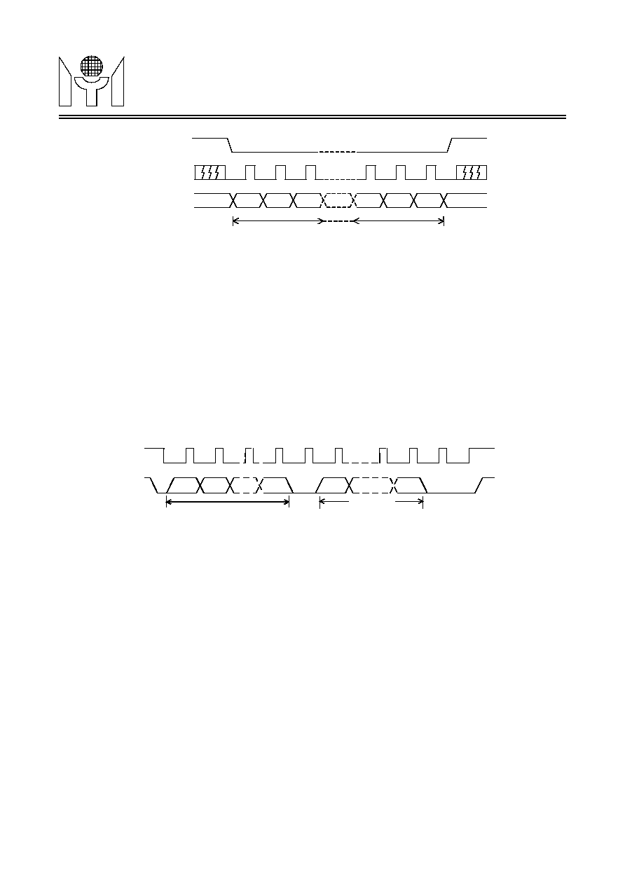
until the last cycle for a complete data packet transfer. The protocol is shown in Figure 1.
SCK
I
8
8
Serial clock input. The clock-input pin is used to synchronize
the data transfer. It has an internal pull-up resistor.
RIN
I
-
9
Red video input. It is used for auto sizing measurement and
this signal is came from video pre-amp red output.
GIN
I
-
10
Green video input. It is used for auto sizing measurement and
this signal is came from video pre-amp green output.
BIN
I
-
11
Blue video input. It is used for auto sizing measurement and
this signal is came from video pre-amp blue output.
NC
-
-
12
No connection.
VDD
-
9
13
Digital power supply. Positive 5 V DC supply for internal digi-
tal circuitry and a 0.1uF decoupling capacitor should be con-
nected across to VDD and VSS.
VFLB
I
10
14
Vertical input. This pin is used to input the vertical synchroniz-
ing signal. It is leading triggered and has an internal pull-up
resistor.
INT
O
11
15
Intensity color output. 16-color selection is achievable by
combining this intensity pin with R/G/B output pins.
FBKG
O
12
16
Fast Blanking output. It is used to cut off external R, G, B sig-
nals of VGA while this chip is displaying characters or win-
dows.
BOUT
O
13
17
Blue color output. It is a blue color video signal output.
GOUT
O
14
18
Green color output. It is a green color video signal output.
ROUT
O
15
19
Red color output. It is a red color video signal output.
VSS
-
16
20
Digital ground. This ground pin is used to internal digital cir-
cuitry.
Name
I/O
Pin No.
Descriptions
16
20
Revision 1.1
-
4-
2001/8/21
MTV038
(Revision 1.1)
MYSON
TECHNOLOGY
There are three transmission formats shown as below:
Format (a) R - C - D -> R - C - D -> R - C - D .....
Format (b) R - C - D -> C - D -> C - D -> C - D .....
Format (c) R - C - D -> D -> D -> D -> D -> D .....
Where R=Row address, C=Column address, D=Display data
3.1.2 I
2
C bus
I
2
C bus operation is only selected when SSB pin is left floating. And a valid transmission should be starting
from writing the slave address 7AH(write mode), or 7BH(read mode) to MTV038. The protocol is shown in
Figure 2. And the auto sizing video measurement data (total 12 bytes) are read only registers and the others
are write only registers.
There are three transmission formats for I
2
C write mode shown as below:
Format (a) S - R - C - D -> R - C - D -> R - C - D .....
Format (b) S - R - C - D -> C - D -> C - D -> C - D .....
Format (c) S - R - C - D -> D -> D -> D -> D -> D .....
Where S=Slave address, R=Row address, C=Column address, D=Display data
And there is one transmission formats for I
2
C read mode shown as below:
Format (a) S -> D -> D -> D -> D -> D -> D -> D -> D -> D -> D -> D -> D -> D -> D -> dummy D .....
Where S=Slave address, D=Measurement data
In the I
2
C read mode, 14 bytes of auto sizing video measurement data will be outputed directly from byte 0 to
byte 9 and continues with dummy data until stop condition occurred when R/W bit is set to 1.
Each arbitrary length of data packet consists of 3 portions viz, Row address (R), Column address (C), and
Display data (D). Format (a) is suitable for updating small amount of data which will be allocated with a differ-
ent row address and column address. Format (b) is recommended for updating data that has the same row
address but a different column address. Massive data updating or full screen data change should use format
(c) to increase transmission efficiency. The row and column address will be incremented automatically when
FIGURE 1. Data Transmission Protocol (SPI)
SCK
SSB
SDA
LSB
MSB
First byte
Last byte
FIGURE 2. Data Transmission Protocol (I
2
C)
SCK
SDA
START
STOP
ACK
ACK
First byte
Last byte
Secondbyte
B7
B6
B0
B7
B0

Revision 1.1
-
5-
2001/8/21
MTV038
(Revision 1.1)
MYSON
TECHNOLOGY
the format (c) is applied. Furthermore, the undefined locations in display or fonts RAM should be filled with
dummy data.
TABLE 1. The Configuration of Transmission Formats
There are 2 types of data which should be accessed through the serial data interface, one is ADDRESS bytes
of display registers, and the other is ATTRIBUTE bytes of display registers, the protocols are same for all
except the bit5 of row address and the bit5 of column address. The MSB(b7) is used to distinguish row and
column addresses when transferring data from external controller. The bit6 of column address is used to dif-
ferentiate the column address for format (a), (b) and format (c) respectively. Bit5 of row address for display
register is used to distinguish ADDRESS byte when it is set to "0" and ATTRIBUTE byte when it is set to "1".
And at address bytes, bit5 of column address is the MSB (bit8) and data bytes are the 8 LSB (bit7~bit0)
of display fonts address to save half MCU memory for true 512 fonts display. So each one of the 512 fonts
can be displayed at the same time (see Table 1). And for format (c), since D8 is filled while program column
address of address bytes, the continued data will be the same bank of upper 256 fonts or lower 256 fonts until
program column address of address bytes again.
The data transmission is permitted to change from format (a) to format (b) and (c), or from format (b) to format
(a) and (c), but not from format (c) back to format (a) and (b). The alternation between transmission formats is
configured as the state diagram shown in Figure 3.
Address
b7
b6
b5
b4
b3
b2
b1
b0
Format
Address Bytes
of Display Reg.
Row
1
0
0
R4
R3
R2
R1
R0
a,b,c
Column
ab
0
0
D8
C4
C3
C2
C1
C0
a,b
Column
c
0
1
D8
C4
C3
C2
C1
C0
c
Data
D7
D6
D5
D4
D3
D2
D1
D0
a,b,c
Attribute Bytes
of Display Reg.
Row
1
0
1
R4
R3
R2
R1
R0
a,b,c
Column
ab
0
0
x
C4
C3
C2
C1
C0
a,b
Column
c
0
1
x
C4
C3
C2
C1
C0
c
Data
D7
D6
D5
D4
D3
D2
D1
D0
a,b,c
Initiate
ROW
COL
c
COL
ab
DA
c
DA
ab
1, X
0, 1
0, 0
X, X
X, X
0, 1
1, X
1, X
format (a)
format (b)
format (c)
X, X
0, X
Input = b7, b6
0, 0
FIGURE 3. Transmission State Diagram