 | –≠–ª–µ–∫—Ç—Ä–æ–Ω–Ω—ã–π –∫–æ–º–ø–æ–Ω–µ–Ω—Ç: MTV118N24 | –°–∫–∞—á–∞—Ç—å:  PDF PDF  ZIP ZIP |

This datasheet contains new product information. Myson Technology reserves the rights to modify the product specification
without notice. No liability is assumed as a result of the use of this product. No rights under any patent accompany the sales of
the product.
1/15
MTV118 Revision 2.0 01/01/1999
MTV118
MYSON
TECHNOLOGY
FEATURES
GENERAL DESCRIPTION
BLOCK DIAGRAM
∑
Horizontal sync input may be up to 120 KHz.
∑
Acceptable wide-range pixel clock up to 96MHz
from XIN pin.
∑
Full-screen display consists of 15 (rows) by 30 (col-
umns) characters.
∑
12 x 18 dot matrix per character.
∑
Total of 256 characters and graphic fonts including
248 mask ROM fonts and 8 programmable RAM
fonts.
∑
8 color selection maximum per display character.
∑
Double character height and/or width control.
∑
Programmable positioning for display screen cen-
ter.
∑
Bordering, shadowing and blinking effect.
∑
Programmable vertical character height (18 to 71
lines) control.
∑
Row to row spacing register to manipulate the con-
stant display height.
∑
4 programmable background windows with multi-
level operation.
∑
Software clears for display frame.
∑
Half tone and fast blanking output.
∑
8-channel/8-bit PWM D/A converter output.
∑
Compatible with SPI bus or I
2
C interface with
address 7AH (slave address is mask option).
∑
16 or 24-pin PDIP/SOP package.
On-Screen-Display for LCD Monitor
MTV118 is designed for LCD monitor
applications to display the built-in characters or
fonts onto an LCD monitor screen. The display
operates by transferring data and control informa-
tion from the micro controller to the RAM through
a serial data interface. It can execute full screen
displays automatically and specific functions such
as character bordering, shadowing, blinking, dou-
ble height and width, font by font color control,
frame positioning, frame size control by character
height and windowing effect. Moreover, MTV118
also provides 8 PWM DAC channels with 8-bit
resolution and a PWM clock output for external
digital-to-analog control.
SERIAL DATA
INTERFACE
ADDRESS BUS
ADMINISTRATOR
VERTICAL
DISPLAY
CONTROL
DISPLAY & ROW
CONTROL
REGISTERS
COLOR
ENCODER
WINDOWS &
FRAME
CONTROL
WR
WG
WB
FBKGC
BLANK
LUMAR
LUMAG
LUMAB
BLINK
VCLKX
DATA
VERTD
HORD
CH
8
8
7
BSEN
SHADOW
OSDENB
HSP
VSP
HORIZONTAL
DISPLAY CONTROL
CLOCK
GENERATOR
8
DATA
LPN
CWS
VCLKS
5
DATA
CWS
CHS
8
LUMAR
LUMAG
LUMAB
BLINK
CRADDR
8
LUMA
BORDER
ARWDB
HDREN
VCLKX
HORD 8
CH
CHS
VERTD
7
8
LPN
NROW
VDREN
5
RCADDR
DADDR
FONTADDR
WINADDR
PWMADDR
5
9
9
5
5
ARWDB
HDREN
VDREN
NROW
DATA
ROW, COL
ACK
8
9
CHARACTER ROM
USER FONT RAM
LUMINANCE &
BORDGER
GENERATOR
VDD
VSS
VDDA
VSSA
ROUT
GOUT
BOUT
FBKG
HTONE
HFLB
NC
XIN
VFLB
SSB
SCK
SDA
VSP
HSP
PWM D/A
CONVERTER
PWM0
PWM1
PWM2
PWM3
PWM4
PWM5
PWM6
PWM7
8
DATA
8
POWER ON
RESET
PRB
2/15
MTV118 Revision 2.0 01/01/1999
MTV118
MYSON
TECHNOLOGY
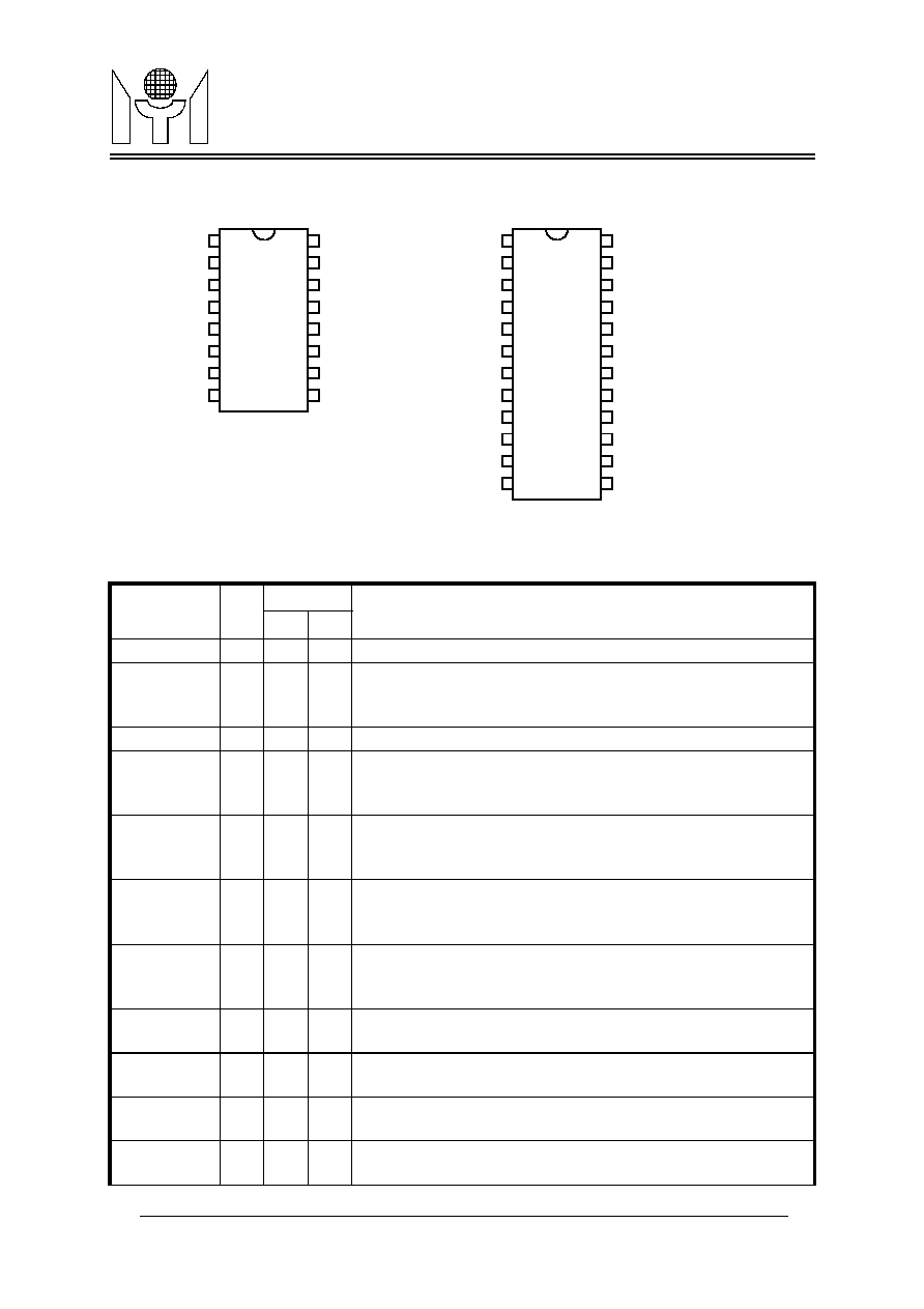
1.0 PIN CONNECTION
2.0 PIN DESCRIPTIONS
Name
I/O
Pin #
Descriptions
N16 N24
VSS
-
1
1
Ground. This ground pin is used for internal circuitry.
XIN
I
2
2
Pixel Clock Input. This is a clock input pin. MTV118 is driven by
an external pixel clock source for all the logics inside. The fre-
quency of XIN must be the integral time of pin HFLB.
NC
I
3
3
No connection.
VDD
-
4
4
Power supply. Positive 5 V DC supply for internal circuitry. A
0.1uF decoupling capacitor should be connected across VDD and
VSS.
HFLB
I
5
5
Horizontal Input. This pin is used to input the horizontal synchro-
nizing signal. It is a leading edge trigger and has an internal pull-
up resistor.
SSB
I
6
6
Serial Interface Enabler. It is used to enable the serial data and
is also used to select the operation of I
2
C or SPI bus. If this pin is
left floating, I
2
C bus is enabled, otherwise the SPI bus is enabled.
SDA
I
7
7
Serial Data Input. The external data transfers through this pin to
internal display registers and control registers. It has an internal
pull-up resistor.
SCK
I
8
8
Serial Clock Input. The clock-input pin is used to synchronize the
data transfer. It has an internal pull-up resistor.
PWM0
O
-
9
Open-Drain PWM D/A Converter 0. The output pulse width is
programmable by the register of row 15, column 19.
PWM1
O
-
10
Open-Drain PWM D/A Converter 1. The output pulse width is
programmable by the register of row 15, column 20.
PWM2
O
-
11
Open-Drain PWM D/A Converter 2. The output pulse width is
programmable by the register of row 15, column 21.
VSS
XIN
NC
VDD
HFLB
SSB
SDA
SCK
VSS
ROUT
GOUT
BOUT
FBKG
HTONE/PWMCK
VFLB
VDD
16
15
14
13
12
11
10
9
1
2
3
4
5
6
7
8
MTV118
VSS
XIN
NC
VDD
HFLB
SSB
SDA
SCK
PWM0
PWM1
PWM2
PWM3
VSS
ROUT
GOUT
BOUT
FBKG
HTONE/PWMCK
VFLB
VDD
PWM7
PWM6
PWM5
PWM4
24
23
22
21
20
19
18
17
16
15
14
13
1
2
3
4
5
6
7
8
9
10
11
12
MTV118N24

3/15
MTV118 Revision 2.0 01/01/1999
MTV118
MYSON
TECHNOLOGY
3.0 FUNCTIONAL DESCRIPTIONS
3.1 Serial Data Interface
The serial data interface receives data transmitted from an external controller. There are 2 types of bus
which can be accessed through the serial data interface: SPI bus and I
2
C bus.
3.1.1 SPI Bus
When the SSB pin is pulled to a HIGH or LOW level, the SPI bus operation is selected. A valid trans-
mission should start from pulling SSB to LOW level, enabling the MTV118 receiving mode and retaining
the LOW level until the last cycle for a complete data packet transfer. The protocol is shown in Figure 1
on page 4.
There are 3 transmission formats as shown below:
Format (a) R - C - D
R - C - D
R - C - D
Format (b) R - C - D
C - D
C - D
C - D
Format (c) R - C - D
D
D
D
D
D
R=row address, C=column address, D=display data
PWM3
O
-
12
Open-Drain PWM D/A Converter 3. The output pulse width is
programmable by the register of row 15, column 22.
PWM4
O
-
13
Open-Drain PWM D/A Converter 4. The output pulse width is
programmable by the register of row 15, column 23.
PWM5
O
-
14
Open-Drain PWM D/A Converter 5. The output pulse width is
programmable by the register of row 15, column 24.
PWM6
O
-
15
Open-Drain PWM D/A Converter 6. The output pulse width is
programmable by the register of row 15, column 25.
PWM7
O
-
16
Open-Drain PWM D/A Converter 7. The output pulse width is
programmable by the register of row 15, column 26.
VDD
-
9
17
Power Supply. Positive 5 V DC supply for internal circuitry and a
0.1uF decoupling capacitor should be connected across VDD and
VSS.
VFLB
I
10
18
Vertical Input. This pin is used to input the vertical synchronizing
signal. It is triggered by lead and has an internal pull-up resistor.
HTONE /
PWMCK
O
11
19
Half Tone Output / PWM Clock Output. This is a multiplexed pin
selected by the PWMCK bit. This pin can be a PWM clock or used
to attenuate R, G, B gain of VGA for the transparent windowing
effect.
FBKG
O
12
20
Fast Blanking Output. It is used to cut off external R, G, B sig-
nals of VGA while this chip is displaying characters or windows.
BOUT
O
13
21
Blue Color Output. This is a blue color video signal output.
GOUT
O
14
22
Green Color Output. This is a green color video signal output.
ROUT
O
15
23
Red Color Output. This is a red color video signal output.
VSS
-
16
24
Ground. This ground pin is used for internal circuitry.
Name
I/O
Pin #
Descriptions
N16 N24

4/15
MTV118 Revision 2.0 01/01/1999
MTV118
MYSON
TECHNOLOGY
3.1.2 I
2
C Bus
I
2
C bus operation is only selected when the SSB pin is left floating. A valid transmission should begin
from writing the slave address 7AH, which is mask option, to MTV118. The protocol is shown in Figure
2 on page 4..
There are 3 transmission formats as shown below:
Format (a) S - R - C - D
R - C - D
R - C - D
Format (b) S - R - C - D
C - D
C - D
C - D
Format (c) S - R - C - D
D
D
D
D
D
S=slave address, R=row address, C=column address, D=display data
Each arbitrary length of data packet consists of 3 portions: row address (R), column address (C) and
display data (D). Format (a) is suitable for updating small amounts of data which will be allocated with
different row and column addresses. Format (b) is recommended for updating data that has the same
row address but a different column address. Massive data updating or full screen data changes should
be done in format (c) to increase transmission efficiency. The row and column addresses will be incre-
mented automatically when format (c) is applied. Furthermore, the undefined locations in display or font
RAM should be filled with dummy data.
There are 3 types of data which should be accessed through the serial data interface: address bytes of
display registers, attribute bytes of display registers and user font RAM data. The protocol is the same
for all except bits 5 and 6 of the row addresses. The MSB(b7) is used to distinguish row and column
addresses when transferring data from an external controller. Bit 6 of the row address is used to distin-
guish display registers and user font RAM data and bit6 of the column address is used to differentiate
the column address for formats (a), (b) and (c), respectively. Bit 5 of the row address for display regis-
ters is used to distinguish the address byte when it is set to "0" and the attribute byte when it is set to
"1". The configuration of transmission formats is shown in Table 1 on page 5.
MS
B
LSB
SSB
SCK
SDA
first byte
last byte
FIGURE 1. Data Transmission Protocol (SPI)
FIGURE 2. Data Transmission Protocol (I
2
C)
SCK
SDA
first byte
START
ACK
second byte
last byte
ACK
STOP
B7
B6
B0
B7
B0

5/15
MTV118 Revision 2.0 01/01/1999
MTV118
MYSON
TECHNOLOGY
The data transmission is permitted to change from format (a) to format (b) and (c), or from format (b) to
format (a), but not from format (c) back to format (a) and (b). The alternation between transmission for-
mats is configured as the state diagram shown in Figure 3 on page 5.
3.2 Address Bus Administrator
The administrator manages bus address arbitration of internal registers or user font RAM during exter-
nal data write-in. The external data write through serial data interface to registers must be synchronized
by internal display timing. In addition, the administrator also provides automatic incrementation to the
address bus when external writing occurs using format (c).
3.3 Vertical Display Control
The vertical display control can generate different vertical display sizes for most display standards in
current monitors. The vertical display size is calculated with the information of a double character height
bit(CHS) and a vertical display height control register(CH6-CH0).The algorithms of a repeating charac-
ter line display are shown in Tables 2 and 3. The programmable vertical size range is 270 lines to max-
imum 2130 lines.
TABLE 1. Configuration of Transmission Formats
Address
b7
b6
b5
b4
b3
b2
b1
b0
Format
Address
Bytes of
Display
Reg.
Row
1
0
0
x
R3
R2
R1
R0
a,b,c
Column
ab
0
0
x
C4
C3
C2
C1
C0
a,b
Column
c
0
1
x
C4
C3
C2
C1
C0
c
Attribute
Bytes of
Display
Reg.
Row
1
0
1
x
R3
R2
R1
R0
a,b,c
Column
ab
0
0
x
C4
C3
C2
C1
C0
a,b
Column
c
0
1
x
C4
C3
C2
C1
C0
c
User
Fonts
RAM
Row
1
1
x
x
x
R2
R1
R0
a,b,c
Column
ab
0
0
C5
C4
C3
C2
C1
C0
a,b
Column
c
0
1
C5
C4
C3
C2
C1
C0
c
Initiate
ROW
COL
c
COL
ab
DA
c
DA
ab
1, X
0, 1
0, 0
X, X
X, X
0, 1
1, X
1, X
format (a)
format (b)
format (c)
X, X
0, X
Input = b7, b6
0, 0
FIGURE 3. Transmission State Diagram