 | –≠–ª–µ–∫—Ç—Ä–æ–Ω–Ω—ã–π –∫–æ–º–ø–æ–Ω–µ–Ω—Ç: AQV252GAX | –°–∫–∞—á–∞—Ç—å:  PDF PDF  ZIP ZIP |
155
Greatly increase load current
(2.5A).
Load voltage is 60V.
cUL
pending
VDE
pending
8.8
.346
6.4
.252
3.9
.154
mm
inch
6.4
.252
3.6
.142
8.8
.346
1
2
3
6
5
4
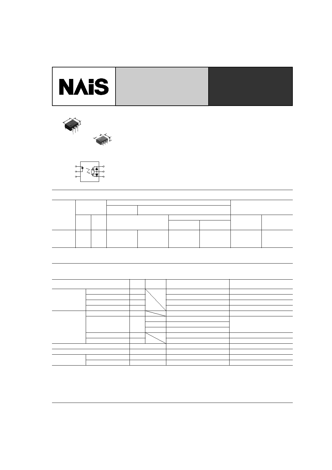
FEATURES
1. Greatly increased load current in the
same package size.
2. Greatly improved specs allow you to
use this in place of mercury and
mechanical relays.
TYPICAL APPLICATIONS
∑ Crime and fire prevention market (use in
I/O for alarm and security devices, etc.)
∑ Measuring instrument market (circuit
testers, etc.)
TYPES
*Indicate the peak AC and DC values.
Note: For space reasons, the SMD terminal shape indicator "A" and the package type indicator "X" and "Z" are omitted from the seal.
Type
Output rating*
Part No.
Packing quantity
Through hole
terminal
Surface-mount terminal
Load
voltage
Load
current
Tube packing style
Tape and reel packing style
Tube
Tape and reel
Picked from the
1/2/3-pin side
Picked from the
4/5/6-pin side
AC/DC type
60 V
2.5 A
AQV252G
AQV252GA
AQV252GAX
AQV252GAZ
1 tube contains
50 pcs.
1 batch contains
500 pcs.
1,000 pcs.
RATING
1. Absolute maximum ratings (Ambient temperature: 25
∞
C
77
∞
F
)
Item
Symbol
Type of
connection
AQV252G(A)
Remarks
Input
LED forward current
I
F
50 mA
LED reverse voltage
V
R
5 V
Peak forward current
I
FP
1 A
f = 100 Hz, Duty factor = 0.1%
Power dissipation
P
in
75 mW
Output
Load voltage (peak AC)
V
L
60 V
Continuous load current
(peak AC)
I
L
A
2.5 A
A connection: Peak AC, DC
B, C connection: DC
B
3.5 A
C
5.0 A
Peak load current
I
peak
6.0 A
100ms (1 shot), V
L
= DC
Power dissipation
P
out
500 mW
Total power dissipation
P
T
550 mW
I/O isolation voltage
V
iso
1,500 V AC
Temperature limits
Operating
T
opr
≠40
∞
C to +85
∞
C
≠40
∞
F to +185
∞
F
Non-condensing at low temperatures
Storage
T
stg
≠40
∞
C to +100
∞
C
≠40
∞
F to +212
∞
F
HE PhotoMOS
(AQV252G)

HE PhotoMOS (AQV252G)
156
2. Electrical characteristics (Ambient temperature: 25
∞
C
77
∞
F
)
Note: Recommendable LED forward current I
F
= 5 to 10 mA.
For type of connection, see Page 34.
*Turn on/Turn off time
Item
Symbol
Type of
connection
AQV252G(A)
Condition
Input
LED operate
current
Typical
I
Fon
--
0.5 mA
I
L
= 100mA
Maximum
3 mA
LED turn off
current
Minimum
I
Foff
--
0.2 mA
I
L
= 100mA
Typical
0.45 mA
LED dropout
voltage
Typical
V
F
--
1.32 V (1.14 V at I
F
= 5 mA)
I
F
= 50 mA
Maximum
1.5 V
Output
On resistance
Typical
R
on
A
0.08
I
F
= 5 mA
I
L
= Max.
Within 1 s on time
Maximum
0.12
Typical
R
on
B
0.04
Maximum
0.06
Typical
R
on
C
0.02
Maximum
0.03
Off state leakage
current
Maximum
I
Leak
--
1
µ
A
I
F
= 0 mA
V
L
= Max.
Transfer
characteristics
Turn on time*
Typical
T
on
--
1.1 ms
I
F
= 5 mA
I
L
= 100 mA
V
L
= 10 V
Maximum
5.0 ms
Turn off time*
Typical
T
off
--
0.25 ms
I
F
= 5 mA
I
L
= 100 mA
V
L
= 10 V
Maximum
0.5 ms
I/O capacitance
Typical
C
iso
--
0.8 pF
f = 1 MHz
V
B
= 0 V
Maximum
1.5 pF
Initial I/O isolation
resistance
Minimum
R
iso
--
1,000 M
500 V DC
Ton
Input
Output
10%
90%
Toff
REFERENCE DATA
1. Load current vs. ambient temperature
characteristics
Allowable ambient temperature: ≠40
∞
C to +85
∞
C
≠40
∞
F to +185
∞
F
2. On resistance vs. ambient temperature
characteristics
Measured portion: between terminals 4 and 6;
LED current: 5 mA; Load voltage: Max. (DC)
Continuous load current: Max.(DC)
3. Turn on time vs. ambient temperature
characteristics
LED current: 5 mA; Load voltage: 10 V (DC);
Continuous load current: 100 mA (DC)
0
6
8
0
20
40
60
80 85 100
≠40 ≠20
2
4
Ambient temperature,
∞C
Load current, A
C connection
B connection
A connection
0
≠40 ≠20
0.2
0
20
40
60
80
Ambient temperature,
∞C
On resistance,
85
0.6
0.8
1
0.4
0
2
Ambient temperature,
∞C
Turn on time, ms
≠40
≠20
5
0
20
40
60
80
1
3
4
85
I
For Dimensions, see Page 29.
I
For Schematic and Wiring Diagrams, see Page 34.
I
For Cautions for Use, see Page 38.

HE PhotoMOS (AQV252G)
157
4. Turn off time vs. ambient temperature
characteristics
LED current: 5 mA; Load voltage: 10 V (DC);
Continuous load current: 100 mA (DC)
5. LED operate current vs. ambient
temperature characteristics
Load voltage: 10 V (DC);
Continuous load current: 100mA (DC)
6. LED turn off current vs. ambient temperature
characteristics
Load voltage: 10 V (DC);
Continuous load current: 100mA (DC)
0
0.4
0.8
0.6
Ambient temperature,
∞C
Turn off time, ms
≠40
≠20
1
0
20
40
60
80
0.2
85
0
2
3
Ambient temperature,
∞C
LED operate current, mA
≠40
≠20
5
0
20
40
60
80 85
1
4
0
2
3
Ambient temperature,
∞C
LED turn off current, mA
≠40
≠20
0
20
40
60
80
1
5
4
85
7. LED dropout voltage vs. ambient
temperature characteristics
LED current: 5 to 50 mA
8. Current vs. voltage characteristics of output
at MOS portion
Measured portion: between terminals 4 and 6;
Ambient temperature: 25
∞
C
77
∞
F
9. Off state leakage current vs. load voltage
characteristics
Measured portion: between terminals 4 and 6;
Ambient temperature: 25
∞
C
77
∞
F
1
1.1
1.2
1.3
1.4
Ambient temperature,
∞C
LED dropout voltage, V
≠40 ≠20
0
20
40
60
80 85
1.5
50mA
30mA
20mA
10mA
5mA
Voltage, V
Current, mA
1
≠1
3
2
≠3
≠2
1
0.5
-1
-0.5
0
30
40
60
Load voltage, V
Off state leakage current, A
10
10
-8
10
-12
10
-10
10
20
10
-6
50
-4
10. Turn on time vs. LED forward current
characteristics
Measured portion: between terminals 4 and 6;
Load voltage: 10 V (DC);
Continuous load current: 100 mA (DC);
Ambient temperature: 25
∞
C
77
∞
F
11. Turn off time vs. LED forward current
characteristics
Measured portion: between terminals 4 and 6;
Load voltage: 10 V (DC);
Continuous load current: 100 mA (DC);
Ambient temperature: 25
∞
C
77
∞
F
12. Output capacitance vs. applied voltage
characteristics
Measured portion: between terminals 4 and 6;
Frequency: 1 MHz;
Ambient temperature: 25
∞
C
77
∞
F
0
1
2
3
5
LED forward current, mA
Turn on time, ms
10
20
30
40
50
4
0
LED forward current, mA
Turn off time, ms
0
0.1
0.3
0.2
10
20
30
40
0.5
50
0
0.4
0
100
200
800
Applied voltage, V
Output capacitance, pF
10
20
30
40
50
500
400
300
600
0
700
60