 | –≠–ª–µ–∫—Ç—Ä–æ–Ω–Ω—ã–π –∫–æ–º–ø–æ–Ω–µ–Ω—Ç: AQV414EA | –°–∫–∞—á–∞—Ç—å:  PDF PDF  ZIP ZIP |
125
TESTING
VDE
(Reinforced type)
(Standard type)
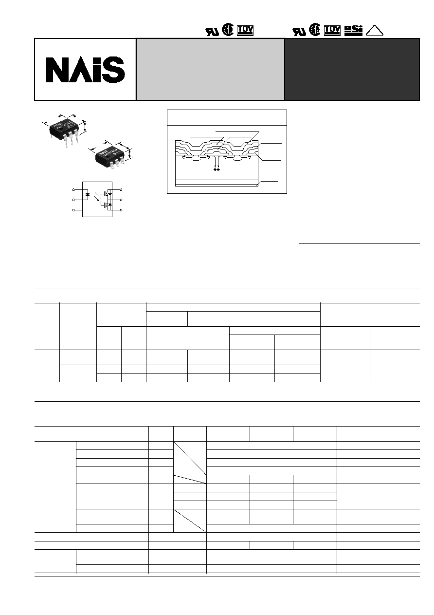
1
2
3
6
5
4
GU (General Use)-E Type
[1-Channel (Form B) Type]
mm
inch
8.8
±
0.05
.346
±
.002
6.4
±
0.05
.252
±
.002
3.6
±
0.2
.142
±
.008
8.8
±
0.05
.346
±
.002
6.4
±
0.05
.252
±
.002
3.9
±
0.2
.154
±
.008
FEATURES
1. Low on resistance for normally-
closed type
This has been realized thanks to the built-
in MOSFET processed by our proprietary
method, DSD (Double-diffused and Se-
lective Doping) method.
,
,
,
,
Source electrode
N≠
N
+
N
+
N
+
P
+
N
+
N
+
P
+
Gate electrode
Passivation membrane
Cross section of the normally-closed type of
power MOS
Intermediate
insulating
membrane
Gate
oxidation
membrane
Drain
electrode
2. Controls low-level analog signals
PhotoMOS relays feature extremely low
closed-circuit offset voltage to enable
control of low-level analog signals without
distortion.
3. High sensitivity, low ON resistance
Can control a maximum 0.13 A load cur-
rent with a 5 mA input current. Low ON re-
sistance of 18
(AQV410EH). Stable
operation because there are no metallic
contact parts.
4. Low-level off state leakage current
The SSR has an off state leakage current
of several milliamperes, whereas the Pho-
toMOS relay has only 100 pA even with
the rated load voltage of 400 V
(AQV414E).
5. Reinforced insulation 5,000 V type
also available.
More than 0.4 mm internal insulation dis-
tance between inputs and outputs. Con-
forms to EN41003, EN60950 (reinforced
insulation).
TYPICAL APPLICATIONS
∑ Security equipment
∑ Telepone equipment (Dial pulse)
∑ Measuring equipment
TYPES
*Indicate the peak AC and DC values.
Note: For space reasons, the package type indicator "X" and "Z" are omitted from the seal.
Type
I/O isolation
voltage
Output rating*
Part No.
Packing quantity
Through hole
terminal
Surface-mount terminal
Load
voltage
Load
current
Tube packing style
Tape and reel packing style
Tube
Tape and reel
Picked from the
1/2/3-pin side
Picked from the
4/5/6-pin side
AC/DC
type
1,500 V AC
(Standard)
400 V
120 mA
AQV414E
AQV414EA
AQV414EAX
AQV414EAZ
1 tube contains
50 pcs.
1 batch contains
500 pcs.
1,000 pcs.
5,000 V AC
(Reinforced)
350 V
130 mA
AQV410EH
AQV410EHA
AQV410EHAX
AQV410EHAZ
400 V
120 mA
AQV414EH
AQV414EHA
AQV414EHAX
AQV414EHAZ
RATING
1. Absolute maximum ratings (Ambient temperature: 25
∞
C
77
∞
F
)
Item
Symbol
Type of
connection
AQV414E(A)
AQV410EH(A)
AQV414EH(A)
Remarks
Input
LED forward current
I
F
50 mA
LED reverse voltage
V
R
3 V
Peak forwrd current
I
FP
1 A
f = 100 Hz, Duty factor = 0.1%
Power dissipation
P
in
75 mW
Output
Load voltage (peak AC)
V
L
400 V
350 V
400 V
Continuous load current
I
L
A
0.12 A
0.13 A
0.12 A
A connection: Peak AC, DC
B,C connection: DC
B
0.13 A
0.15 A
0.13 A
C
0.15 A
0.17 A
0.15 A
Peak load current
I
peak
0.3 A
0.4 A
0.3 A
A connection: 100 ms (1 shot),
V
L
= DC
Power dissipation
P
out
500 mW
Total power dissipation
P
T
550 mW
I/O isolation voltage
V
iso
1,500 V AC
5,000 V AC
5,000 V AC
Temperature
limits
Operating
T
opr
≠40
∞
C to +85
∞
C
≠40
∞
F to +185
∞
F
Non-condensing at low
temperatures
Storage
T
stg
≠40
∞
C to +100
∞
C
≠40
∞
F to +212
∞
F
PhotoMOS
RELAYS
AQV414E, AQV41
r
EH
126
2. Electrical characteristics (Ambient temperature: 25
∞
C
77
∞
F
)
For type of connection, see Page 32.
Note: Recommendable LED forward current
Standard type I
F
= 5 mA
Reinforced type I
F
= 5 to 10 mA
*Operate/Reverse time
Item
Symbol
Type of
connec-
tion
AQV414E(A)
AQV410EH(A)
AQV414EH(A)
Condition
Input
LED operate (OFF) current
Typical
I
Foff
--
1.45 mA
1.9 mA
1.75 mA
I
L
= Max.
Maximum
3.0 mA
LED reverse (ON) current
Minimum
I
Fon
--
0.3 mA
0.4 mA
0.3 mA
I
L
= Max.
Typical
1.40 mA
1.8 mA
1.70 mA
LED dropout voltage
Typical
V
F
--
1.14 V (1.25 V at I
F
= 50 mA)
I
F
= 5 mA
Maximum
1.5 V
Output
On resistance
Typical
R
on
A
26
18
25.2
I
F
= 0 mA
I
L
= Max.
Within 1 s on time
Maximum
50
35
50
Typical
R
on
B
20
13
19
I
F
= 0 mA
I
L
= Max.
Within 1 s on time
Maximum
25
17.5
25
Typical
R
on
C
10
6.5
10
I
F
= 0 mA
I
L
= Max.
Within 1 s on time
Maximum
12.5
8.8
12.5
Off state leakage current
Maximum
I
Leak
--
1
µ
A
10
µ
A
10
µ
A
I
F
= 5 mA
V
L
= Max.
Transfer
characteristics
Switching
speed
Operate
(OFF) time*
Typical
T
off
--
0.7 ms
1.5 ms
1.3 ms
I
F
= 0 mA
®
5 mA
I
L
= Max.
Maximum
2.0 ms
3.0 ms
3.0 ms
Reverse
(ON) time*
Typical
T
on
--
0.1 ms
0.3 ms
0.3 ms
I
F
= 5 mA
®
0 mA
I
L
= Max.
Maximum
1.0 ms
1.5 ms
1.5 ms
I/O capacitance
Typical
C
iso
--
0.8 pF
0.8 pF
0.8 pF
f = 1 MHz
V
B
= 0
Maximum
1.5 pF
Initial I/O isolation
resistance
Minimum
R
iso
--
1,000 M
500 V DC
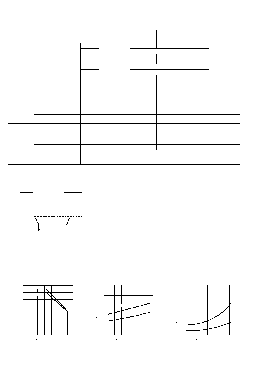
Toff
Input
Output
10%
90%
Ton
s
For Dimensions, see Page 27.
s
For Schematic and Wiring Diagrams, see Page 32.
s
For Cautions for Use, see Page 36.
REFERENCE DATA
1. Load current vs. ambient temperature char-
acteristics
Allowable ambient temperature: ≠40
∞
C to +85
∞
C
≠40
∞
F to +185
∞
F
Type of connection: A
2. On resistance vs. ambient temperature char-
acteristics
Measured portion: between terminals 4 and 6;
LED current: 0 mA; Load voltage: Max. (DC);
Continuous load current: Max. (DC)
3. Operate (OFF) time vs. ambient temperature
characteristics
LED current: 5mA; Load voltage: Max. (DC);
Continuous load current: Max. (DC)
Ambient temperature,
∞
C
Load current, mA
0
40
60
80
100
140
120
0
20
40
60
80
100
≠40 ≠20
20
85
AQV410EH
AQV414E(H)
Ambient temperature,
∞
C
On resistance,
0
10
20
30
40
≠40
≠20
50
0
20
40
60
8085
AQV410EH
AQV414(EH)
Ambient temperature,
∞
C
Operate (OFF) time, ms
0
2.0
3.0
≠40
≠20
5.0
0
20
40
60
80
1.0
4.0
85
AQV410EH
AQV414E
AQV414EH
AQV414E, AQV41
r
EH
127
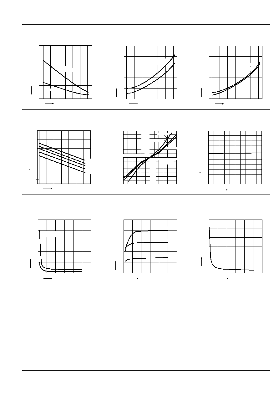
4. Reverse (ON) time vs. ambient temperature
characteristics
LED current: 5 mA; Load voltage: Max. (DC);
Continuous load current: Max. (DC)
5. LED operate (OFF) current vs. ambient tem-
perature characteristics
Load voltage: Max. (DC);
Continuous load current: Max. (DC)
6. LED reverse (ON) current vs. ambient tem-
perature characteristics
Load voltage: Max. (DC);
Continuous load current: Max. (DC)
Ambient temperature,
∞
C
Reverse (ON) time, ms
0
≠20
≠40
20
40
60
80 85
0.8
0.6
0.4
0.2
0
AQV410EH
AQV414E
AQV414EH
Ambient temperature,
∞
C
LED operate (OFF) curremt, mA
0
1
2
3
4
≠40
≠20
5
0
20
40
60
8085
AQV410EH
AQV414E
AQV414EH
Ambient temperature,
∞
C
LED reverse (ON) current, mA
0
1
2
3
4
≠40
≠20
5
0
20
40
60
80 85
AQV410EH
AQV414E
AQV414EH
7. LED dropout voltage vs. ambient tempera-
ture characteristics
LED current: 5 to 50 mA
8. Voltage vs. current characteristics of output
at MOS portion
Measured portion: between terminals 4 and 6;
Ambient temperature: 25
∞
C
77
∞
F
9. Off state leakage current
Measured portion: between terminals 4 and 6;
LED current: 5 mA; Ambient temperature: 25
∞
C
77
∞
F
Ambient temperature,
∞
C
LED dropout voltage, V
0
≠40
≠20
20
40
60
80 85
1.5
1.4
1.3
1.2
1.1
1.0
0
50mA
30mA
20mA
10mA
5mA
20
40
60
80
140
120
100
≠3
≠2
≠1
≠2.5
≠1.5
≠0.5
0.5
3
1.5
2.5
1
2
≠20
≠40
≠60
≠80
≠100
≠120
≠140
AQV410EH
AQV414E
AQV414EH
Current, mA
Voltage, V
Load voltage, V
Off state leakage current, A
20
0
60
40
80
100
10
≠3
10
≠6
10
≠9
10
≠12
10. LED forward current vs. operate (OFF) time
characteristics
Measured portion: between terminals 4 and 6;
Load voltage: Max. (DC); Continuous load current:
Max. (DC); Ambient temperature: 25
∞
C
77
∞
F
11. LED forward current vs. reverse (ON) time
characteristics
Measured portion: between terminals 4 and 6;
Load voltage: Max. (DC); Continuous load current:
Max. (DC); Ambient temperature: 25
∞
C
77
∞
F
12. Applied voltage vs. output capacitance
characteristics
Measured portion: between terminals 4 and 6;
Frequency: 1 MHz;
Ambient temperature: 25
∞
C
77
∞
F
LED forward current, mA
Operate (OFF) time, ms
0
2.0
4.0
6.0
8.0
10.0
10
20
30
40
50
AQV414E
AQV410EH
AQV414EH
LED forward current, mA
Reverse (ON) time, ms
10
20
30
40
50
60
10
0
20
30
40
50
60
0.5
0.4
0.3
0.2
0.1
0
AQV414E
AQV410EH
AQV414EH
Applied voltage, V
Output capacitance, pF
0
20
40
100
10
20
30
40
50
60
80
120
5/7/2001
All Rights Reserved, © Copyright Matsushita Electric Works, Ltd.
Go To Online Catalog