 | –≠–ª–µ–∫—Ç—Ä–æ–Ω–Ω—ã–π –∫–æ–º–ø–æ–Ω–µ–Ω—Ç: AQV414SX | –°–∫–∞—á–∞—Ç—å:  PDF PDF  ZIP ZIP |
66
1
2
3
6
5
4
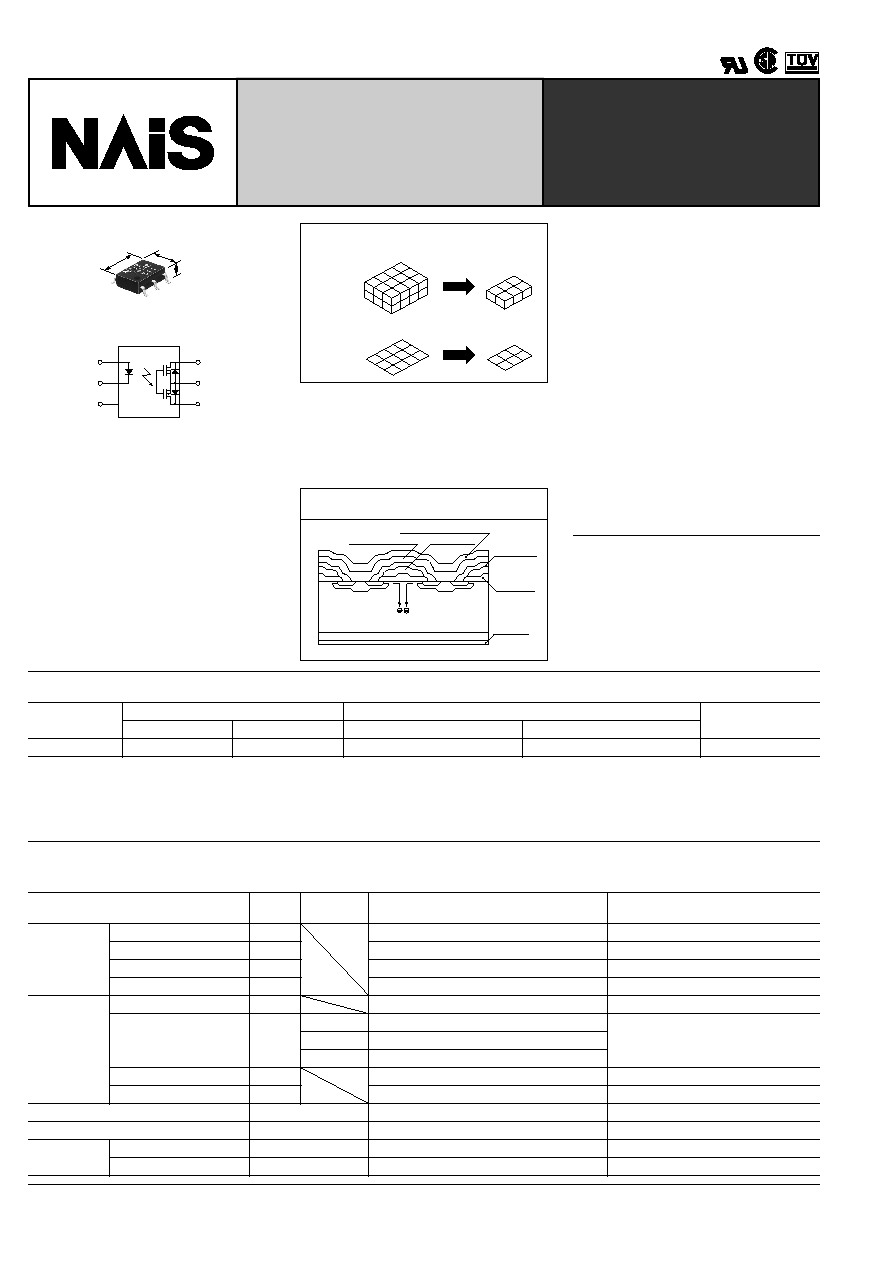
GU (General Use) Type
SOP Series
[1-Channel (Form B) Type]
mm
inch
6.3
±
0.2
.248
±
.008
4.4
±
0.2
.173
±
.008
2.1
±
0.2
.083
±
.008
FEATURES
1. 1 channel (Form B) in super minia-
ture design
The device comes in a super-miniature
SO package measuring (W) 4.4
◊
(L) 6.3
◊
(H) 2.1 mm
(W) .173
◊
(L) .248
◊
(H) .083
inch
--approx. 25% of the volume and
50% of the footprint size of DIP type Pho-
toMOS Relays.
Volume
(SOP)
(DIP)
Approx. 25%
Footprint
Approx. 50%
2. Low on resistance (Max. 50
) at 400
V for normally-closed type
has been achieved thanks to the built-in
MOSFET processed by our proprietary
method, DSD (Double-Diffused and Se-
lective Doping) method.
,
,
,
Source electrode
N≠
N
+
N
+
N
+
P
+
N
+
N
+
P
+
Gate electrode
Passivation membrane
Cross section of the normally-closed type of
power MOS
Intermediate
insulating
membrane
Gate
oxidation
membrane
Drain
electrode
3. Tape and reel
The device comes standard in a tape and
reel (1,000 pcs./reel) to facilitate automat-
ic insertion machines.
4. Controls low-level analog signals
PhotoMOS relays feature extremely low
closed-circuit offset voltage to enable
control of low-level analog signals without
distortion.
5. Low-level off state leakage current
In contrast to the SSR with an off state
leakage current of several milliamps, the
PhotoMOS relay features a very small off
state leakage current of only 100 pA even
at the rated load voltage of 400 V.
6. Low thermal electromotive force
(Approx. 1
µ
V)
TYPICAL APPLICATIONS
∑ Telephones
∑ Measuring instruments
∑ Computer
∑ Industrial robots
∑ High-speed inspection machines
TYPES
*Indicate the peak AC and DC values.
Notes: (1) Tape package is the standard packing style. Also available in tube. (Part No. suffix "X" ro "Z" is not needed when ordering; Tube: 75 pcs.;
Case: 1,500 pcs.)
(2) For space reasons, the top two letters of the product number "AQ" are ommitted on the product seal. The package type indicator "X" and "Z"
are also omitted from the seal. (Ex. the label for product number AQV414S is V414S).
Type
Output ratings*
Part No.
Packing quantity in
tape and reel
Load voltage
Load current
Picked from the 1/2/3-pin side
Picked from the 4/5/6-pin side
AC/DC
400 V
100 mA
AQV414SX
AQV414SZ
1,000 pcs.
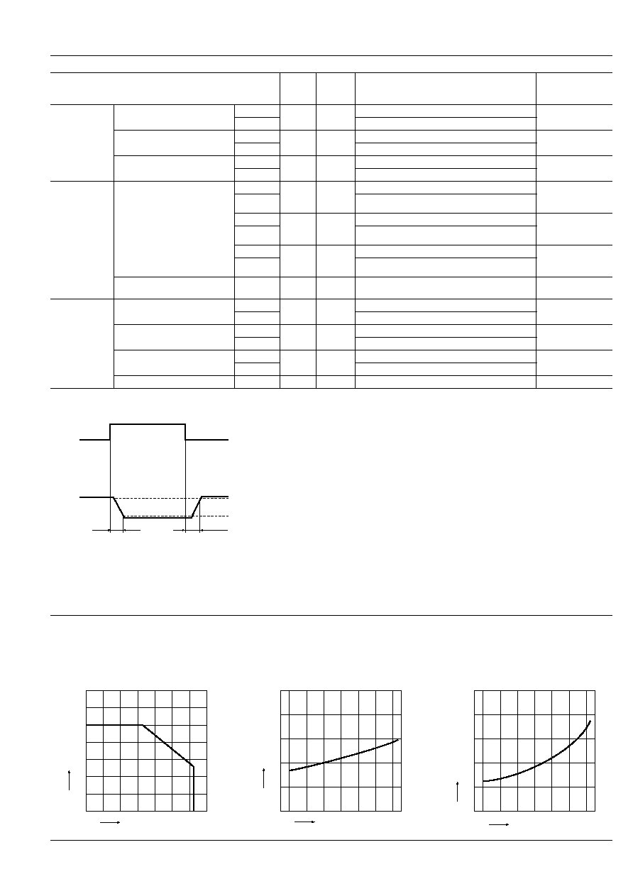
RATING
1. Absolute maximum ratings (Ambient temperature: 25
∞
C
77
∞
F
)
Item
Symbol
Type of
connection
AQV414S
Remarks
Input
LED forward current
I
F
50 mA
LED reverse voltage
V
R
3 V
Peak forward current
I
FP
1 A
f = 100 Hz, Duty factor = 0.1%
Power dissipation
P
in
75 mW
Output
Load voltage (peak AC)
V
L
400 V
Continuous load current
I
L
A
0.10 A
A connection: Peak AC, DC
B,C connection: DC
B
0.11 A
C
0.12 A
Peak load current
I
peak
0.3 A
A connection: 100 ms (1 shot) V
L
= DC
Power dissipation
P
out
450 mW
Total power dissipation
P
T
500 mW
I/O isolation voltage
V
iso
1,500 V AC
Temperature
limits
Operating
T
opr
≠40
∞
C to +85
∞
C
≠40
∞
F to +185
∞
F
Non-condensing at low temperatures
Storage
T
stg
≠40
∞
C to +100
∞
C
≠40
∞
F to +212
∞
F
PhotoMOS
RELAYS
AQV414S
67
2. Electrical characteristics (Ambient temperature: 25
∞
C
77
∞
F
)
Note: Recommendable LED forward current I
F
= 5mA.
For type of connection, see page 32.
*Turn on/Turn off time
s
For Dimensions, see Page 28.
s
For Schematic and Wiring Diagrams, see Page 32.
s
For Cautions for Use, see Page 36.
Item
Symbol
Type of
connec-
tion
AQV414S
Remarks
Input
LED operate current
Typical
I
Fon
--
0.6 mA
I
L
= Max.
Maximum
3 mA
LED turn off current
Minimum
I
Foff
--
0.4 mA
I
L
= Max.
Typical
0.55 mA
LED dropout voltage
Typical
V
F
--
1.14 V (1.25 V at I
F
= 50 mA)
I
F
= 5 mA
Maximum
1.5 V
Output
On resistance
Typical
R
on
A
26
I
F
= 5 mA
I
L
= Max.
Within 1 s on time
Maximum
50
Typical
R
on
B
20
I
F
= 5 mA
I
L
= Max.
Within 1 s on time
Maximum
25
Typical
R
on
C
10
I
F
= 5 mA
I
L
= Max.
Within 1 s on time
Maximum
12.5
Off state leakage current
Maximum
I
Leak
--
1
µ
A
I
F
= 0
V
L
= Max.
Transfer
characteristics
Turn on time*
Typical
T
on
--
0.47 ms
I
F
= 5 mA
V
L
= Max.
Maximum
1.0 ms
Turn off time
Typical
T
off
--
0.28 ms
I
F
= 5 mA
V
L
= Max.
Maximum
1.0 ms
I/O capacitance
Typical
C
iso
--
0.8 pF
f = 1 MHz
V
B
= 0
Maximum
1.5 pF
Initial I/C isolation resistance
Minimum
R
iso
--
1,000 M
500 V DC
Toff
Input
Output
10%
90%
Ton
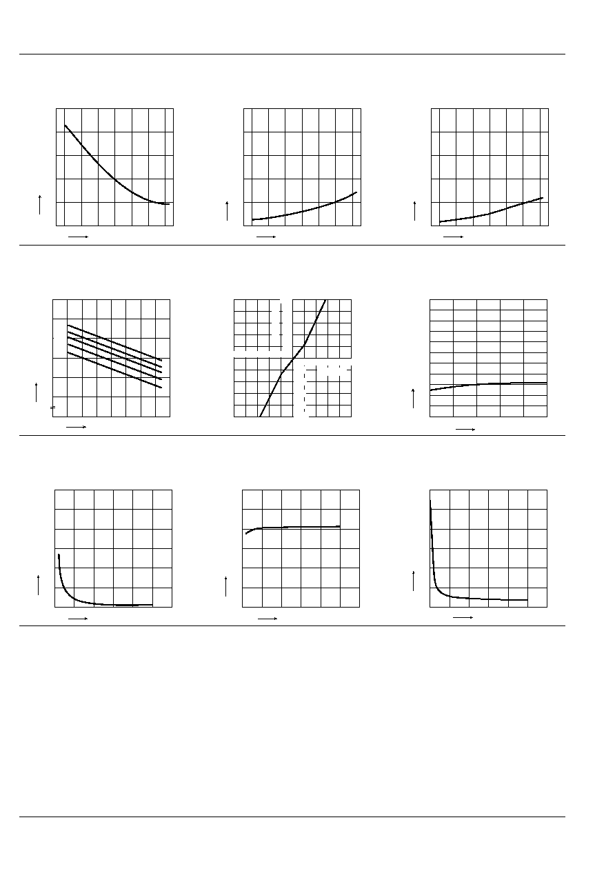
REFERENCE DATA
1. Load current vs. ambient temperature char-
acteristics
Allowable ambient temperature: ≠40
∞
C to +85
∞
C
≠40
∞
F to +185
∞
F
Type of connection: A
2. On resistance vs. ambient temperature char-
acteristics
Measured portion: between terminals 4 and 6;
LED current: 0 mA;
Continuous load current: 100 mA (DC)
3. Operate (OFF) time vs. ambient temperature
characteristics
LED current: 5 mA;
Load voltage: 400 V (DC);
Continuous load current: 100 mA (DC)
≠40 ≠20
8085 100
120
100
80
60
40
20
0
140
0
20
40
60
100
120
100
80
60
40
20
0
140
Load current, mA
Ambient temperature,
∞
C
0
20
40
60
80 85
50
40
30
20
10
0
≠40
≠20
On resistance,
Ambient temperature,
∞
C
0
≠40
≠20
20
40
60
8085
1.0
0.8
0.6
0.4
0.2
0
Operate (OFF) time, ms
Ambient temperature,
∞
C
AQV414S
68
4. Reverse (ON) time vs. ambient temperature
characteristics
LED current: 50 mA;
Load voltage: 400 V (DC);
Continuous load current: 100 mA (DC)
5. LED operate (OFF) current vs. ambient tem-
perature characteristics
Load voltage: 400 V (DC);
Continuous load current: 100 mA (DC)
6. LED reverse (ON) current vs. ambient tem-
perature characteristics
Load voltage: 400 V (DC);
Continuous load current: 100 mA (DC)
0
≠40
≠20
20
40
60
8085
1.0
0.8
0.6
0.4
0.2
0
Reverse (ON) time, ms
Ambient temperature,
∞
C
0
≠40
≠20
20
40
60
8085
5
4
3
2
1
0
LED operate (OFF) current, mA
Ambient temperature,
∞
C
-20
0
20
60
40
80 85
5
4
3
2
1
0
≠40
LED operate (ON) current, mA
Ambient temperature,
∞
C
7. LED dropout voltage vs. ambient tempera-
ture characteristics
LED current: 5 to 50 mA
8. Voltage vs. current characteristics of output
at MOS portion
Measured portion: between terminals 4 and 6;
Ambient temperature: 25
∞
C
77
∞
F
9. Off state leakage current
Measured portion: between terminals 4 and 6;
LED current: 5 mA;
Ambient temperature: 25
∞
C
77
∞
F
50m
30m
20m
10m
5mA
≠40
-20
0
20
40
60
80
100
85
1.5
1.4
1.3
1.2
1.1
1.0
0
LED drop out voltage, V
Ambient temperature,
∞
C
20
40
60
80
100
≠20
≠40
≠60
≠80
≠100
≠5 ≠4 ≠3 ≠2 ≠1
1
2
3
4
5
Voltage,V
Current, mA
20
0
60
40
80
100
10
≠3
10
≠6
10
≠9
10
≠12
Load voltage, V
Off state leakage current, A
10. LED forward current vs. operate (OFF) time
characteristics
Measured portion: between terminals 4 and 6;
Load voltage: 400 V (DC); Continuous load current:
100 mA (DC); Ambient temperature: 25
∞
C
77
∞
F
11. LED forward current vs. reverse (ON) time
characteristics
Measured portion: between terminals 4 and 6;
Load voltage: 400 V (DC); Continuous load current:
100 mA (DC); Ambient temperature: 25
∞
C
77
∞
F
12. Applied voltage vs. output capacitance
characteristics
Measured portion: between terminals 4 and 6;
Frequency: 1 MHz;
Ambient temperature: 25
∞
C
77
∞
F
10
20
30
40
50
60
3.0
2.5
2.0
1.5
1.0
0.5
0
Operate (OFF) time, ms
LED forward current, mA
10
20
30
40
50
60
10
20
30
40
50
60
0.6
0.5
0.4
0.3
0.2
0.1
0
Reverse (ON) time, ms
LED forward current, mA
10
20
30
40
50
60
120
100
80
60
40
20
0
Output capacitance, pF
Applied voltage, V
5/7/2001
All Rights Reserved, © Copyright Matsushita Electric Works, Ltd.
Go To Online Catalog