 | –≠–ª–µ–∫—Ç—Ä–æ–Ω–Ω—ã–π –∫–æ–º–ø–æ–Ω–µ–Ω—Ç: AQW454A | –°–∫–∞—á–∞—Ç—å:  PDF PDF  ZIP ZIP |
168
1
2
3
4
8
7
6
5
High sensitivity and low
on-resistance.
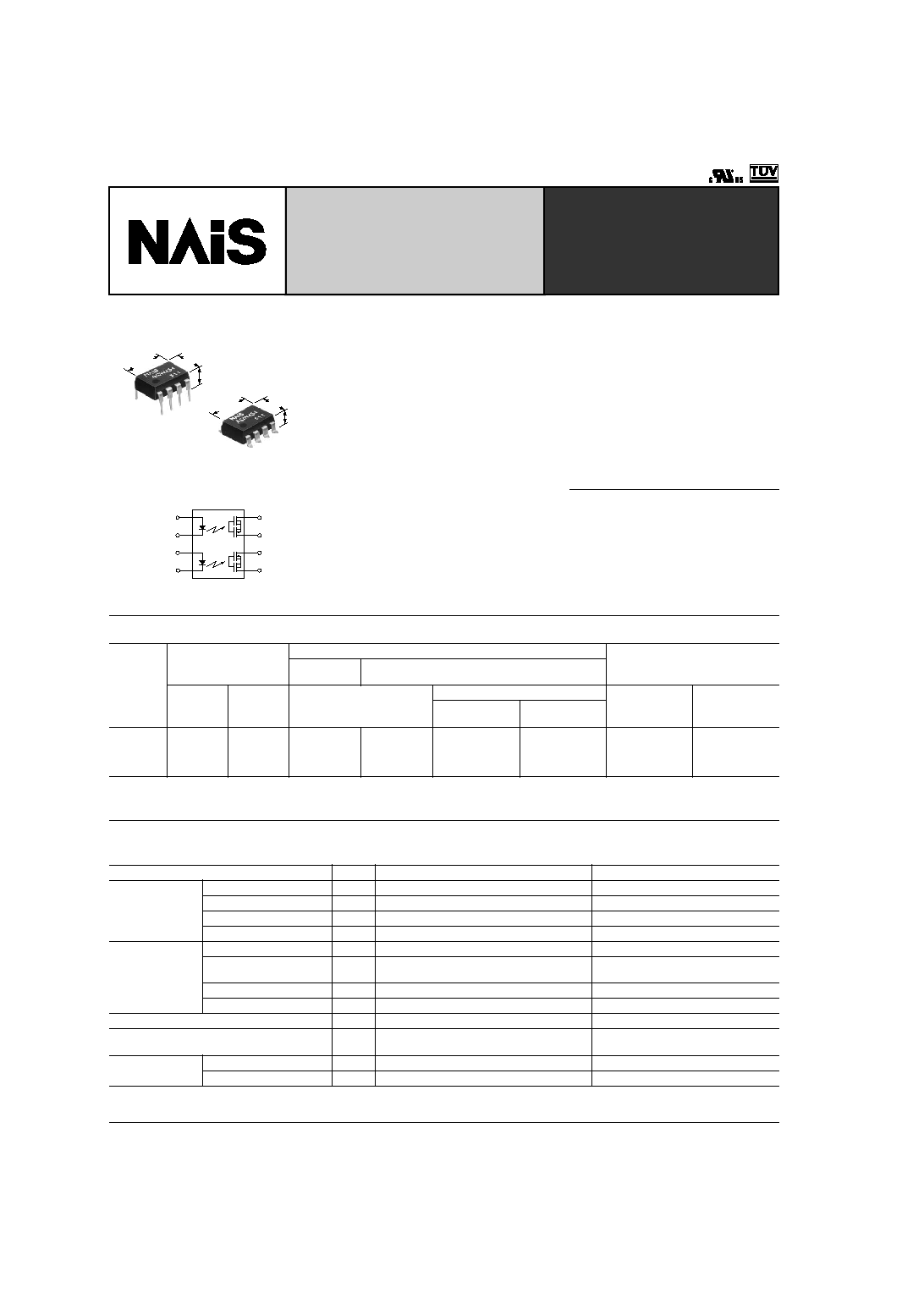
DIP (2 Form B) 8-pin type.
mm
inch
9.78
.385
6.4
.252
3.9
.154
9.78
.385
6.4
.252
3.6
.142
FEATURES
1. Compact 8-pin DIP size
The device comes in a compact (W)
6.4
◊
(L) 9.78
◊
(H) 3.9 mm (W) .
252
◊
(L)
.385
◊
(H) .154 inch
, 8-pin DIP size
(through hole terminal type).
2. Applicable for 2 Form B use as well
as two independent 1 Form B use.
3. Controls low-level analog signals
PhotoMOS relays feature extremely low
closed-circuit offset voltage to enable
control of low-level analog signals without
distortion.
4. High sensitivity, low ON resistance
Can control a maximum 0.16 A (AQW454)
load current with a 5 mA input current.
Low ON resistance of 16
(AQW454).
Stable operation because there are no
metallic contact parts.
5. Low-level off state leakage current
The SSR has an off state leakage current
of several miliamperes, whereas the
PhotoMOS relay has only 100 pA even
with the rated load voltage of 400 V
(AQW454).
6. Low thermal electromotive force
(Approx. 1
µ
V)
TYPICAL APPLICATIONS
∑ Security equipment
∑ High-speed inspection machine
∑ Measuring equipment
∑ Telecommunication equipment
∑ Sensors
TYPES
*Indicate the peak AC and DC values.
Note: For space reasons, the SMD terminal shape indicator "A" and the package type indicator "X" and "Z" are omitted from the seal.
Type
Output rating*
Part No.
Packing quantity
Through hole
terminal
Surface-mount terminal
Load
voltage
Load
current
Tube packing style
Tape and reel packing style
Tube
Tape and reel
Picked from the
1/2/3/4-pin side
Picked from the
5/6/7/8-pin side
AC/DC
400 V
120 mA
AQW454
AQW454A
AQW454AX
AQW454AZ
1 tube contains
40 pcs.
1 batch contains
400 pcs.
1,000 pcs
RATING
1. Absolute maximum ratings (Ambient temperature: 25
∞
C
77
∞
F
)
Item
Symbol
AQW454(A)
Remarks
Input
LED forward current
I
F
50 mA
LED reverse voltage
V
R
5 V
Peak forward current
I
FP
1 A
f = 100 Hz, Duty factor = 0.1%
Power dissipation
P
in
75 mW
Output
Load voltage (peak AC)
V
L
400 V
Continuous load current
I
L
0.12 A (0.16 A)
A connection: Peak AC, DC
( ): for one 1b-circuit
Peak load current
I
peak
0.36 A
A connection: 100 ms (1 shot), V
L
= DC
Power dissipation
P
out
800 mW
Total power dissipation
P
T
850 mW
I/O isolation voltage
V
iso
1,500 V AC
Between input and output/between
contact sets
Temperature limits
Operating
T
opr
≠40
∞
C to +85
∞
C
≠40
∞
F to +185
∞
F
Non-condensing at low temperatures
Storage
T
stg
≠40
∞
C to +100
∞
C
≠40
∞
F to +212
∞
F
HE PhotoMOS
(AQW454)

HE PhotoMOS (AQW454)
169
2. Electrical characteristics (Ambient temperature: 25
∞
C
77
∞
F
)
Note: Recommendable LED forward current I
F
= 5 mA. For type of connection, see page 36.
*Operate/Reverse time
I
For Dimensions, see Page 29.
I
For Schematic and Wiring Diagrams, see Page 36.
I
For Cautions for Use, see Page 38.
Item
Symbol
AQW454(A)
Condition
Input
LED operate (OFF) current
Typical
I
Foff
0.9 mA
I
L
= Max.
Maximum
3 mA
LED reverse (ON) current
Minimum
I
Fon
0.4 mA
I
L
= Max.
Typical
0.8 mA
LED dropout voltage
Typical
V
F
1.25 V (1.14 V at I
F
= 5 mA)
I
F
= 50 mA
Maximum
1.5 V
Output
On resistance
Typical
R
on
11
I
F
= 0 mA
I
L
= Max.
Within 1 s on time
Maximum
16
Off state leakage current
Maximum
I
Leak
1
µ
A
I
F
= 5 mA
V
L
= Max.
Transfer char-
acteristics
Switching
speed
Operate (OFF)
time*
Typical
T
off
1.2 ms
I
F
= 0 mA
5 mA
I
L
= Max.
Maximum
2 ms
Reverse (ON)
time*
Typical
T
on
0.36 ms
I
F
= 5 mA
0 mA
I
L
= Max.
Maximum
1 ms
I/O capacitance
Typical
C
iso
0.8 pF
f = 1 MHz
V
B
= 0 V
Maximum
1.5 pF
Initial I/O isolation resistance
Minimum
R
iso
1,000 M
500 V DC
Toff
Input
Output
10%
90%
Ton
REFERENCE DATA
1. Load current vs. ambient temperature
characteristics
Allowable ambient temperature: ≠40
∞
C to +85
∞
C
≠40
∞
F to +185
∞
F
2. On resistance vs. ambient temperature
characteristics
Measured portion: between terminals 5 and 6,
7 and 8; LED current: 0 mA; Load voltage: 400 V (DC);
Continuous load current: 120 mA (DC)
3. Operate (OFF) time vs. ambient temperature
characteristics
LED current: 5 mA; Load voltage: 400 V (DC);
Continuous load current: 120 mA (DC)
0
150
200
250
0
20
40
60
≠20
8085 100
≠40
100
50
Ambient temperature,
∞C
Load current, mA
8
≠40
12
0
≠20
20
40
60
8085
16
14
10
Ambient temperature,
∞C
On resistance,
0
1
2
5
≠40
3
0
≠20
20
40
60
8085
4
Ambient temperature,
∞C
Operate (OFF) time, ms

HE PhotoMOS (AQW454)
170
4. Reverse (ON) time vs. ambient temperature
characteristics
LED current: 5 mA; Load voltage: 400 V (DC);
Continuous load current: 120 mA (DC)
5. LED operate (OFF) current vs. ambient
temperature characteristics
Load voltage: 400 V (DC);
Continuous load current: 120 mA (DC)
6. LED reverse (ON) current vs. ambient
temperature characteristics
Load voltage: 400 V (DC);
Continuous load current: 120 mA (DC)
0
0.5
1.0
1.5
2.5
≠40
0
≠20
20
40
60
8085
2.0
Ambient temperature,
∞C
Reverse (ON) time, ms
0
1
2
3
≠40
5
0
≠20
20
40
60
8085
4
Ambient temperature,
∞C
LED operate (OFF) current, mA
0
1
2
3
≠40
5
0
≠20
20
40
60
8085
4
Ambient temperature,
∞C
LED reverse (ON) current, mA
7. LED dropout voltage vs. ambient
temperature characteristics
LED current: 5 to 50 mA
8. Current vs. voltage characteristics of output
at MOS portion
Measured portion: between terminals 5 and 6,
7 and 8; Ambient temperature: 25
∞
C
77
∞
F
9. Off state leakage current vs. load voltage
characteristics
Measured portion: between terminals 5 and 6,
7 and 8; Ambient temperature: 25
∞
C
77
∞
F
0
1.0
1.1
1.2
1.3
≠40
0
≠20
20
40
60
8085
1.4
50mA
30mA
20mA
10mA
5mA
Ambient temperature,
∞C
LED dropout voltage, V
3
2
1
0
≠3
≠2
≠1
150
100
50
≠150
≠100
≠50
Current, mA
Voltage, V
0
100
10
≠3
10
≠6
10
≠9
10
≠12
20
40
60
80
Load voltage, V
Off state leakage current, A
10. Operate (OFF) time vs. LED forward
current characteristics
Measured portion: between terminals 5 and 6, 7 and
8; Load voltage: 400 V (DC); Continuous load current:
120 mA (DC); Ambient temperature: 25
∞
C
77
∞
F
11. Reverse (ON) time vs. LED forward current
characteristics
Measured portion: between terminals 5 and 6, 7 and
8; Load voltage: 400 V (DC); Continuous load current:
120 mA (DC); Ambient temperature: 25
∞
C
77
∞
F
12. Output capacitance vs. applied voltage
characteristics
Measured portion: between terminals 5 and 6, 7 and
8; Frequency: 1 MHz;
Ambient temperature: 25
∞
C
77
∞
F
0
1
2
3
4
5
10
20
30
40
50
60
0
LED forward current, mA
Operate (OFF) time, ms
0
0.2
0.4
0.6
1.0
0.8
10
20
30
40
50
60
0
LED forward current, mA
Reverse (ON) time, ms
0
200
10
20
30
40
50
60
0
100
Applied voltage, V
Output capacitance, pF