 | –≠–ª–µ–∫—Ç—Ä–æ–Ω–Ω—ã–π –∫–æ–º–ø–æ–Ω–µ–Ω—Ç: AQY212GH | –°–∫–∞—á–∞—Ç—å:  PDF PDF  ZIP ZIP |

PhotoMOS
RELAYS
GU (General Use) Type
1-Channel (Form A)
High Capacity 4-Pin Type
cUL
pending
VDE
pending
mm
inch
4.78
.188
6.4
.252
3.2
.126
1
2
4
3
FEATURES
1. Greatly increased load current.
2. Reinforced insulation 5,000 V type.
3. Greatly improved specs allow you to
use this in place of mercury and
mechanical relays.
4. Compact 4-pin DIP size.
TYPICAL APPLICATIONS
∑ Security market
(use in I/O for alarm and security devices,
etc.)
∑ Measuring instrument market
TYPES
*Indicate the peak AC and DC values.
Note: For space reasons, the initial letters of the product number "AQY", the SMD terminal shape indicator "A" and the package type indicator "X" and
"Z" are omitted from the seal.
Type
I/O isolation
voltage
Output rating*
Part No.
Packing quantity
Through hole
terminal
Surface-mount terminal
Load
voltage
Load
current
Tube packing style
Tape and reel packing style
Tube
Tape and reel
Picked from the
1/2-pin side
Picked from the
3/4-pin side
AC/DC
type
Reinforced
5,000 V
60 V
1.1 A
AQY212GH
AQY212GHA
AQY212GHAX
AQY212GHAZ
1 tube contains
100 pcs.
1 batch contains
1,000 pcs.
1,000 pcs.
RATING
1. Absolute maximum ratings (Ambient temperature: 25
∞
C
77
∞
F
)
Item
Symbol
AQY212GH
Remarks
Input
LED forward current
I
F
50 mA
LED reverse voltage
V
R
5 V
Peak forward current
I
FP
1 A
f = 100 Hz, Duty factor = 0.1%
Power dissipation
P
in
75 mW
Output
Load voltage (peak AC)
V
L
60 V
Continuous load current
(peak AC)
I
L
1.1 A
Peak load current
I
peak
3.0 A
100ms (1 shot), V
L
= DC
Power dissipation
P
out
500 mW
Total power dissipation
P
T
550 mW
I/O isolation voltage
V
iso
5,000 V AC
Temperature limits
Operating
T
opr
≠40
∞
C to +85
∞
C
≠40
∞
F to +185
∞
F
Non-condensing at low temperatures
Storage
T
stg
≠40
∞
C to +100
∞
C
≠40
∞
F to +212
∞
F
AQY212GH.fm1
y [ W Q O O Q N U
S oe @ j oe @
™ P Q
Q T "

AQY212GH
2
2. Electrical characteristics (Ambient temperature: 25
∞
C
77
∞
F
)
Note: Recommendable LED forward current I
F
= 5 to 10 mA.
For type of connection, see Page 4.
*Turn on/Turn off time
Item
Symbol
AQY212GH
Condition
Input
LED operate
current
Typical
I
Fon
1.1 mA
I
L
= 100mA
Maximum
3 mA
LED turn off
current
Minimum
I
Foff
0.3 mA
I
L
= 100mA
Typical
1.0 mA
LED dropout
voltage
Typical
V
F
1.14 V (1.32 V at IF = 50 mA)
I
F
= 5 mA
Maximum
1.5 V
Output
On resistance
Typical
R
on
0.34
I
F
= 5 mA
I
L
= Max.
Within 1 s on time
Maximum
0.7
Off state leakage
current
Maximum
I
Leak
1
µ
A
I
F
= 0
V
L
= Max.
Transfer
characteristics
Turn on time*
Typical
T
on
1.3 ms
I
F
= 5 mA
I
L
= 100 mA
V
L
= 10 V
Maximum
5.0 ms
Turn off time*
Typical
T
off
0.1 ms
I
F
= 5 mA
I
L
= 100 mA
V
L
= 10 V
Maximum
0.5 ms
I/O capacitance
Typical
C
iso
0.8 pF
f = 1 MHz
V
B
= 0
Maximum
1.5 pF
Initial I/O isolation
resistance
Minimum
R
iso
1,000 M
500 V DC
Ton
Input
Output
10%
90%
Toff
REFERENCE DATA
1. Load current vs. ambient temperature
characteristics
Allowable ambient temperature: ≠40
∞
C to +85
∞
C
≠40
∞
F to +185
∞
F
2. On resistance vs. ambient temperature
characteristics
Measured portion: between terminals 3 and 4;
LED current: 5 mA; Load voltage: Max. (DC)
Continuous load current: Max.(DC)
3. Turn on time vs. ambient temperature
characteristics
LED current: 5 mA; Load voltage: 10 V (DC);
Continuous load current: 100 mA (DC)
0
1
2
Ambient temperature,
∞
C
Load current, A
2.5
3
0
20
40
60
8085 100
≠40 ≠20
0.5
1.5
0
≠40 ≠20
0.2
0
20
40
60
80
Ambient temperature,
∞
C
On resistance,
85
0.6
0.8
1
0.4
0
2
Ambient temperature,
∞
C
Turn on time, ms
≠40
≠20
5
0
20
40
60
80
1
3
4
85
AQY212GH.fm2
y [ W Q O O Q N U
S oe @ j oe @
™ P Q
Q T "

AQY212GH
3
4. Turn off time vs. ambient temperature
characteristics
LED current: 5 mA; Load voltage: 10 V (DC);
Continuous load current: 100 mA (DC)
5. LED operate current vs. ambient
temperature characteristics
Load voltage: 10 V (DC);
Continuous load current: 100mA (DC)
6. LED turn off current vs. ambient temperature
characteristics
Load voltage: 10 V (DC);
Continuous load current: 100mA (DC)
0
0.4
0.8
0.6
Ambient temperature,
∞
C
Turn off time, ms
≠40
≠20
1
0
20
40
60
80
0.2
85
0
2
3
Ambient temperature,
∞
C
LED operate current, mA
≠40
≠20
5
0
20
40
60
80 85
1
4
0
2
3
Ambient temperature,
∞
C
LED turn off current, mA
≠40
≠20
0
20
40
60
80
1
5
4
85
7. LED dropout voltage vs. ambient
temperature characteristics
LED current: 5 to 50 mA
8. Voltage vs. current characteristics of output
at MOS portion
Measured portion: between terminals 3 and 4;
Ambient temperature: 25
∞
C
77
∞
F
9. Off state leakage current
Measured portion: between terminals 3 and 4;
Ambient temperature: 25
∞
C
77
∞
F
1
1.1
1.2
1.3
1.4
Ambient temperature,
∞
C
LED dropout voltage, V
≠40 ≠20
0
20
40
60
80 85
1.5
50mA
30mA
20mA
10mA
5mA
Voltage, V
Current, mA
1
≠1
3
2
≠3
≠2
1
0.5
≠1
≠0.5
0
30
40
60
Load voltage, V
Off state leakage current, A
10
10
-12
10
-10
10
20
10
-6
10
-8
50
-4
10. LED forward current vs. turn on time
characteristics
Measured portion: between terminals 3 and 4;
Load voltage: 10 V (DC);
Continuous load current: 100 mA (DC);
Ambient temperature: 25
∞
C
77
∞
F
11. LED forward current vs. turn off time
characteristics
Measured portion: between terminals 3 and 4;
Load voltage: 10 V (DC);
Continuous load current: 100 mA (DC);
Ambient temperature: 25
∞
C
77
∞
F
12. Applied voltage vs. output capacitance
characteristics
Measured portion: between terminals 3 and 4;
Frequency: 1 MHz;
Ambient temperature: 25
∞
C
77
∞
F
0
1
2
3
5
LED forward current, mA
Turn on time, ms
10
20
30
40
50
4
0
LED forward current, mA
Turn off time, ms
0
0.1
0.3
0.2
10
20
30
40
0.5
50
0
0.4
0
100
200
800
Applied voltage, V
Output capacitance, pF
10
20
30
40
50
500
400
300
600
0
700
60
AQY212GH.fm3
y [ W Q O O Q N U
S oe @ j oe @
™ P Q
Q T "

AQY212GH
4
DIMENSIONS
mm
inch
Through hole terminal type
Terminal thickness = 0.2
.008
General tolerance:
±
0.1
±
.004
Surface mount terminal type
Terminal thickness = 0.2
.008
General tolerance:
±
0.1
±
.004
4.78
.188
6.4
.252
2.7
.106
7.62
±
0.05
.300
±
.002
Max. 10
∞
Max. 10
∞
1.0
.039
0.33
.013
0.2
.008
3.0
.118
0.47
.019
3.2
±
0.1
.126
±
.004
0.47
.019
2.54
.100
4.78
.188
6.4
.252
1.0
.039
2.7
.106
7.62
±
0.05
.300
±
.002
Max. 10
∞
1.0
.039
1.0
.039
2.7
.106
0.47
.019
0.47
.019
2.54
.100
0.2
.008
±
0.2
0
±
.008
0
PC board pattern (BOTTOM VIEW)
Tolerance:
±
0.1
±
.004
Mounting pad (TOP VIEW)
Tolerance:
±
0.1
±
.004
4-0.8 dia.
4-.031 dia.
7.62
.300
6.4
.252
2.54
.100
2.54
.100
8.3
.327
1.9
.075
1.5
.059
2.54
.100
SCHEMATIC AND WIRING DIAGRAMS
Notes: E
1
: Power source at input side; I
F
: LED forward current; V
L
: Load voltage; I
L
: Load current;
Schematic
Output
configura-
tion
Load
Connec-
tion
Wiring diagram
1a
AC/DC
--
1
2
4
3
1
IF
IL
2
3
4
VL (AC,DC)
Load
Load
IL
4
3
VL (AC,DC)
E1
AQY212GH.fm4
y [ W Q O O Q N U
S oe @ j oe @
™ P Q
Q T "
AQY212GH
5
Cautions for Use
SAFETY WARNINGS
∑ Do not use the product under conditions
that exceed the range of its specifications.
It may cause overheating, smoke, or fire.
∑ Do not touch the recharging unit while
the power is on. There is a danger of
electrical shock. Be sure to turn off the
power when performing mounting,
maintenance, or repair operations on the
relay (including connecting parts such as
the terminal board and socket).
∑ Check the connection diagrams in the
catalog and be sure to connect the
terminals correctly. Erroneous
connections could lead to unexpected
operating errors, overheating, or fire.
NOTES
1. Short across terminals
Do not short circuit between terminals
when relay is energized. There is
possibility of breaking the internal IC.
2. Surge voltages at the input
If reverse surge voltages are present at
the input terminals, connect a diode in
reverse parallel across the input terminals
and keep the reverse voltages below the
reverse breakdown voltage.
3. Recommended LED forward current
(I
F
)
It is recommended that the LED forward
current (I
F
) be kept at 5mA.
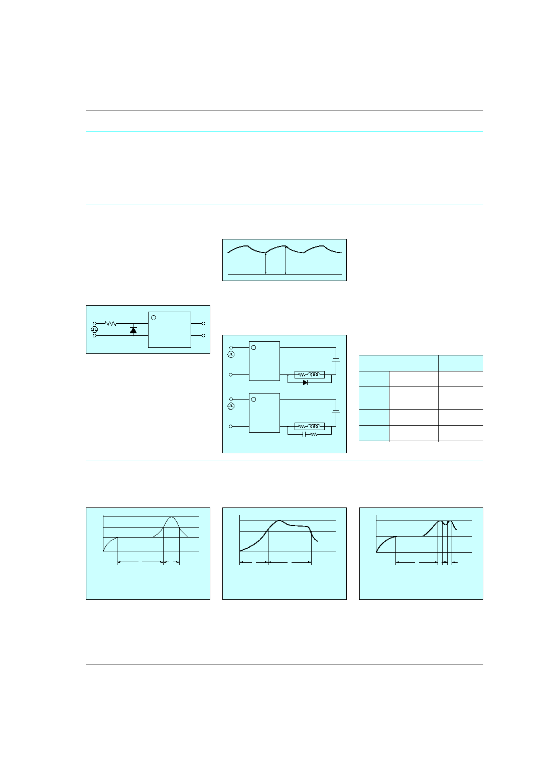
4. Ripple in the input power supply
If ripple is present in the input power
supply, observe the following:
1) For LED operate current at E
min
,
maintain the value mentioned in the table
of "Note 3. Recommended LED forward
current (I
F
)."
2) Keep the LED operate current at 50
mA or less at E
max
.
5. Output spike voltages
1) If an inductive load generates spike
voltages which exceed the absolute
maximum rating, the spike voltage must
be limited.
Typical circuits are shown below.
2) If spike voltages generated at the load
are limited with a clamp diode and the
circuit wires are long, spike voltages will
occur by inductance. Keep wires as short
as possible to minimize inductance.
6. Cleaning solvents compatibility
Dip cleaning with an organic solvent is
recommended for removal of solder flux,
dust, etc. Select a cleaning solvent from
the following table. If ultrasonic cleaning is
used, the severity of factors such as
frequency, output power and cleaning
solvent selected may cause loose wires
and other defects. Make sure these
conditions are correct before use. For
details, please consult us.
1
2
4
3
E
min.
E
max.
1
2
4
Load
Add a clamp diode
to the load
Add a CR snubber
circuit to the load
Load
3
1
2
4
3
Cleaning solvent
Compatibility
(
r
: Yes
!
: No)
Chlorine-
base
∑ Trichlene
∑ Chloroethlene
r
Adueous
∑ Indusco
∑ Hollis
∑ Lonco Terg
r
Alcohol-
base
∑ IPA
∑ Ethanol
r
Others
∑ Thinner
∑ Gasoline
!
7. Soldering
1) When soldering PC board terminals,
keep soldering time to within 10 s at
260
∞
C
500
∞
F
.
2) When soldering surface-mount
terminals, the following conditions are
recommended.
(1) IR (Infrared reflow) soldering method
(2) Vapor phase soldering method
(3) Double wave soldering method
T
1
T
2
T
3
T
1
= 155 to 165
∞
C
311 to 329
∞
F
T
2
= 180
∞
C 200
∞
C
356 to 392
∞
F
T
3
= 245
∞
C
473
∞
F
or less
t
1
= 120 s or less
t
2
= 30 s or less
t
1
t
2
T
2
T
1
t
1
t
2
T
1
= 180 to 200
∞
C
366 to 392
∞
F
T
2
= 215
∞
C
419
∞
F
or less
t
1
= 40 s
t
2
= 90 s or less
T
2
T
1
t
1
t
2
t
3
T
1
= 155 to 165
∞
C
311 to 329
∞
F
T
2
= 260
∞
C
500
∞
F
or less
t
1
= 60 s or less
t
2+
t
3
= 5 s or less
(4) Soldering iron method
Tip temperature: 280 to 300
∞
C
536 to
572
∞
F
Wattage: 30 to 60 W
Soldering time: within 5 s
(5) Others
Check mounting conditions before using
other soldering methods (hot-air, hot
plate, pulse heater, etc.)
∑ The temperature profile indicates the
temperature of the soldered terminal on
the surface of the PC board. The ambient
temperature may increase excessively.
Check the temperature under mounting
conditions.
∑ The conditions for the infrared reflow
soldering apply when preheating using
the VPS method.
AQY212GH.fm5
y [ W Q O O Q N U
S oe @ j oe @
™ P Q
Q T "