
Subject
Chip Resistor Array PRODUCT SPECIFICATION FOR INFORMATION
Spec. No.
151-EXB-28V02DE
Part No.
EXB28V
EXB28V
EXB28V
EXB28V
9
9
9
9----1111
MATSUSHITA ELECTRONIC COMPONENTS Co.,LTD.
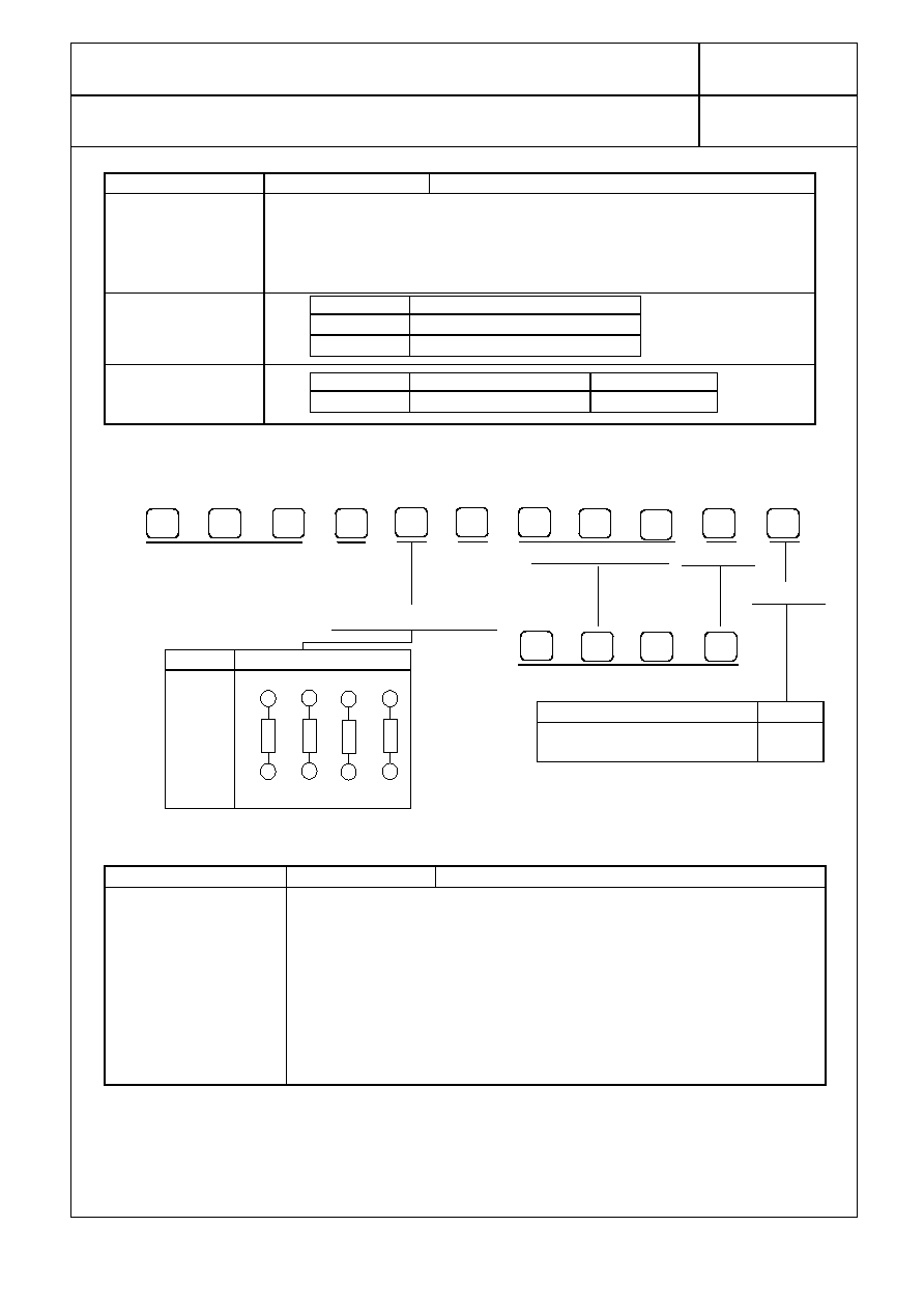
1.
Dimension
L
W
T
A
B
Dimension(mm)
2.00
±
0.10
1.00
±
0.10
0.35
±
0.05
0.20
±
0.10
0.20
±
0.10
P
G
Dimension(mm)
0.50
±
0.10
0.25
±
0.10
2.
Power derating curve
100
80
60
40
20
0
20
0
120
100
-40 -20
-60
80
60
40
140 160
-55
∞
C
70
∞
C
125
∞
C
Ambient Temperature(
∞
C)
Fig. 1
%
o
f
ra
t
e
d di
ss
i
p
a
t
i
o
n
Category temperature range
-55
∞
C to +125
∞
C
3.
Ratings
Item
Rated Value
Explanation
0.031 W / element
When used at ambient temperature over 70
∞
C,
the rated dissipation should be reduced as shown
in Fig.1
Rated Dissipation
Chip jumper : Rated current 1 A (Resistance is less than 50 m
)
Rated voltage
&
Rated Continuous
Working Voltage
(RCWV)
The rated voltage of each resistor should be calculated from the
equation below, and when the rated voltage exceeds the limiting
element voltage, the limiting element voltage should the maximum
working voltage.
E = P
◊
R Limiting element voltage : 50 V
E: Rated voltage(V), P: Rated dissipation(W), R: Rated resistance(
))
(1)Substrate
(2)Protective
coating
(3)Resistive
element
Alumina
Resin
Ruthenium oxide
(4)Termination
(Inner)
(5)Termination
(Between)
(6) Termination
(Outer)
Ag or Ag/Pd
Side:Resin+Metal
Ni Plating
Sn or Sn/ Pb
Plating
A
P
T
W
B
L
B
G
G
(0.3)
(0.2)
a
a'
(1) (2) (3) (4) (5) (6)
a-a' sectional plan
Subject
Chip Resistor Array PRODUCT SPECIFICATION FOR INFORMATION
Spec. No.
151-EXB-28V02DE
Part No.
EXB28V
EXB28V
EXB28V
EXB28V
9
9
9
9----2222
MATSUSHITA ELECTRONIC COMPONENTS Co.,LTD.
Item
Rated Value
Explanation
Maximum
overload voltage
Voltage should be 2.5
◊
E. When the voltage exceeds the maximum
overload voltage, the value shown below should be the maximum
overload voltage.
Maximum overload voltage: 100V
Chip jumper: Max. overload current 2A
Resistance
tolerance
Range of rated
resistance for
manufacture
4.
Explanation of part number
E
X
B
2
8
V
1
0
2
J
X
Thick Film
Resistor Networks
Chip
Resistor
Array
Isolated
Circuit
Rated Resistance Tolerance
Packaging
Number of terminals
R
0
0
0
Chip Jumper
5.
Appearance & Construction
Item
Specifications
Explanation
Appearance &
Construction
1. The resistive element should be covered with protective coating
that do not fade easily. The surface of coating should avoid
unevenness, flaw, pinhole and discoloration.
2. The electrode should be printed uniformly, as shown in the
dimensions. The plating should not fade easily, and should avoid
unevenness, flaw, pinhole, projection and discoloration.
3. The electrode should be connected electrically, mechanically to
resistive element.
4. Substrate should not have chipping, flaw, flash and crack. Details
of appearance criteria shall be as described in attached sheet
sign
Tolerance for resistance
J
±
5%
0
Chip Jumper
Part No.
28V
Circuit
1
2
3
4
8
7
6
5
Packaging
Code
Standard Taping
(2mm pitch, 10,000pcs/reel)
X
Tolerance
Resistance range
Series
J
1.0
to 1.0 M
E-24
Subject
Chip Resistor Array PRODUCT SPECIFICATION FOR INFORMATION
Spec. No.
151-EXB-28V02DE
Part No.
EXB28V
EXB28V
EXB28V
EXB28V
9
9
9
9----3333
MATSUSHITA ELECTRONIC COMPONENTS Co.,LTD.
As far as there shall be not designation especially, the following test and measurement shall be
operated under normal temperature(5
∞
C to 35
∞
C), normal humidity(45 %RH to 85 %RH),
normal atmospheric pressure(86 kPa to 106 kPa).
6.
Performance Specification
Specification
Item
Resistor
Jumper
Test methods
DC resistance
DC resistance value shall be
within the specified tolerance
Measuring voltage: refer to JIS-C5201-1
At 20
∞
C, 65 %RH
Resistance
TCR
<
10
◊
10
-6
/
∞
C
10
to 1M
±
200
◊
10
-6
/
∞
C
Temperature
coefficient
Natural resistance change per temperature
degree centigrade.
R
2
- R
1
R
1
◊
(t
2
- t
1
)
R
1
: Resistance value at reference
temperature(t
1
)
R
2
: Resistance value at test
temperature(t
2
)
t
2
- t
1
= 100
∞
C, t
1
= 25
∞
C
Overload
±
(2 %+0.1
)
Less than
50 m
Resistors shall be applied 2.5 times the rated
voltage for 5 seconds.
Maximum over load voltage shall be 100 V.
Intermittent
overload
±
(5 %+0.1
)
Less than
50 m
Resistors shall be subjected to 10000 cycles of
2.5 times the rated voltage applied for 1
second with pause of 25 seconds between
tests.
Maximum over load voltage shall be 100 V
Dielectric
Withstanding
No evidence of flashover,
mechanical damage, arcing or
insulation breakdown.
AC 100V between substrate and termination
for 1 minute.
Insulation
Resistance
Min. 1,000 M
Insulation resistance between substrate and
termination shall be measured at DC 100V.
7.
Mechanical characteristic
Specification
Item
Resistor
Jumper
Test methods
Terminal strength min. 4.9N
Copper plate: t=0.4 mm
Pull speed: 10 mm/s
No mechanical damage
Bend strength of
the face plating
±
(1 %+0.05
)
Less than
50 m
Substrate: Glass epoxy(t = 1.6 mm)
Span: 90 mm
Bending distance: 3 mm (10 seconds)
Solderability
Termination should be covered
uniformly with solder.
(min. 95 % coverage)
Resistors shall be dipped in the melted solder
bath at 235
∞
C
±
5
∞
C for 2 s
±
0.5 s. Flux shall
be removed from the surface of termination
with clean organic solvent.
TCR=
+600
-
100
Subject
Chip Resistor Array PRODUCT SPECIFICATION FOR INFORMATION
Spec. No.
151-EXB-28V02DE
Part No.
EXB28V
EXB28V
EXB28V
EXB28V
9
9
9
9----4444
MATSUSHITA ELECTRONIC COMPONENTS Co.,LTD.
Specification
Item
Resistor
Jumper
Test methods
Resistance to
soldering heat
±
(1 %+0.05
)
Less than
50 m
Resistors shall be dipped in the melted solder
bath at 270
∞
C
±
5
∞
C for 10s
±
1s.
Vibration
±
(1 %+0.05
)
Less than
50 m
Resistors shall be subjected to a single
vibration having as double amplitude of 1.5
mm for 2 hours in each three mutually
perpendicular directions for total 6 hours.
The vibration frequency shall be varied
uniformly 10 Hz to 55 Hz and return to 10 Hz
traversing for 1 minute.
Without distinct deformation in
appearance
Solvent resistance
±
(0.5 %+0.05
)
Less than
50 m
Solvent solution: Isopropyl alcohol
(1) Dipping 10 hours
±
1 hour, dry in room
condition for 30 min
±
10 min.
(2) Ultrasonic wave washing: 5 min
±
1 min
(0.3 W/cm,28 kHz)
Dry in room condition for 30 min
±
10 min.
8.
Environmental Test
Specification
Item
Resistor
Jumper
Test methods
Low temperature
exposure
±
(1 %+005
)
Less than
50 m
Resistors shall be exposed at -55
∞
C
±
3
∞
C for
1000 hours hours
Low temperature
operating
±
(1 %+0.05
)
Less than
50 m
Resistors shall be placed at -65
∞
C
±
5
∞
C for
1.5hours. After applying RCWV for 45
minutes, resistors shall be exposed in room
condition for 8 hours
±
1 hour.
Endurance at upper
category
temperature
±
(1 %+0.05
)
Less than
50 m
Resistors shall be exposed at +125
∞
C
±
3
∞
C for
1000 hours hours.
Temperature
cycling
±
(1 %+0.05
)
Less than
50 m
-55
∞
C
±
3
∞
C, 30 minutes
Nominal temp., 30minutes 25cycles
+125
∞
C
±
3
∞
C, 30minutes
Humidity
(Steady state)
±
(1 %+0.05
)
Less than
50 m
Resistors shall be exposed at 60
∞
C
±
2
∞
C and
90 % to 95 % relative humidity in a humidity
test chamber for 1000 hours hours.
Salt spray
±
(1 %+0.05
)
Less than
50 m
Spray 5 wt%
±
1 wt% salt water for 96 hours
±
4 hours at 35
∞
C
±
2
∞
C
Endurance at 70
∞
C
±
(3 %+0.1
)
Less than
50 m
Resistors shall be exposed at 70
∞
C
±
2
∞
C for
1000 hours hours. During this time, the
rated voltage shall be applied intermittently
for 1.5 hours ON, 0.5 hour OFF.
Load life in
Humidity
±
(3 %+0.1
)
Less than
50 m
Resistor shall be exposed at 60
∞
C
±
2
∞
C and
90 % to 95 % relative humidity for 1000 hours
hours. During this time, the rated voltage
shall be applied intermittently for 1.5 hours
ON, 0.5 hour OFF.
+48
0
+48
0
+48
0
+48
0
+48
0

Subject
Chip Resistor Array PRODUCT SPECIFICATION FOR INFORMATION
Spec. No.
151-EXB-28V02DE
Part No.
EXB28V
EXB28V
EXB28V
EXB28V
9
9
9
9----5555
MATSUSHITA ELECTRONIC COMPONENTS Co.,LTD.
9.
Other characteristics
Item
Specification
Test methods
Surface
temperature rise
Less than 30
∞
C
Resistor shall be mounted on grass epoxy
substrate (t = 1.0 mm). A power of 0.031 W /
element shall be applied. The temperature
rise at the center of resistor is measured.
However, applied voltage must not exceed
max. overload voltage.
10.
Resistance value marking
No marking.

Subject
Chip Resistor Array PRODUCT SPECIFICATION FOR INFORMATION
Spec. No.
151-EXB-28V02DE
Part No.
EXB28V
EXB28V
EXB28V
EXB28V
9
9
9
9----6666
MATSUSHITA ELECTRONIC COMPONENTS Co.,LTD.
11.
Notice for use
Notice for use
(1)This specification shows the quality and performance of the product in a unit component. Before
adoption, be sure to evaluate and verify the product mounting it in your product.
(2)We take no responsibility for troubles caused by the product usage that is not specified in this
specification.
(3)In traffic transportation equipment (trains, cars, traffic signal equipment, etc.), medical
equipment, aerospace equipment, electric heating appliances, combustion and gas equipment,
rotating equipment, disaster and crime preventive equipment, etc. in cases where it is forecast
that the failure of this product gives serious damage to human life and others, use fail-safe design
and ensure safety by studying the following items to
!
Ensure safety as the system by setting protective circuits and protective equipment.
!
Ensure safety as the system by setting such redundant circuits as do not cause danger by a
single failure.
(4)When a dogma shall be occurred about safety for this product, be sure to inform us rapidly, operate
your technical examination.
(5)The products in this specification are tended for use in general standard applications for general
electric equipment (AV products, household electric appliances, office equipment, information and
communication equipment, etc.); hence, they do not take the use under the following special
environments into consideration.
Accordingly, the use in the following special environments, and such environmental conditions
may affect the performance of the products; prior to use, verify the performance, reliability, etc.
thoroughly.
1) Use in liquids such as water, oil, chemical and organic solvent.
2) Use under direct sunlight or in outdoor or dusty atmospheres
3) Use in places full of corrosive gases such as sea breeze, Cl
2
, H
2
S, NH
3
, SO
2
, and NO
X
4) Use in environment with large static electricity or strong electromagnetic waves.
5) Where the product is close to a heating component, or where an inflammable such as a polyvinyl
chloride wire is arranged close to the product.
6) Where the resistor is sealed or coated with resin , etc.
7) Where water or a water-soluble detergent is used in flux cleaning after soldering (pay particular
attention to water-soluble flux.)
(6)If transient load (heavy load on a short time) like pulse is expected to be applied, carry out
evaluation and confirmation test with resistors actually mounted on your own board. When the
load of more than rated power is applied under the load condition at steady state, it may impair
performance and/or reliability of resistor. Never exceed the rated power.
When the product shall be used under special condition, be sure to ask us in advance.
(7)Halogen type (chlorine type, bromine type, etc.) or other high-activity flux is not recommended as
the residue may affect performance or reliability of resistors.
(8)When soldering with soldering iron, never touch the body of the chip resistor with a tip of the
soldering iron. When using a soldering iron with a tip at high temperature, solder for a time as
short as possible. (Three seconds or less up to 350
∞
C)
(9)Avoid physical shock to the resistor and nipping of the resistor with hard tool (a pair of pliers or
tweezers) as it may damage protective firm or the body of resistor and may affect resistor's
performance.
(10)Reflow soldering method shall apply to this product in principle.
!

Subject
Chip Resistor Array PRODUCT SPECIFICATION FOR INFORMATION
Spec. No.
151-EXB-28V02DE
Part No.
EXB28V
EXB28V
EXB28V
EXB28V
9
9
9
9----7777
MATSUSHITA ELECTRONIC COMPONENTS Co.,LTD.
12.
Storage method
If the product is stored in the following environments and conditions, the performance and
solderability may be badly affected. Avoid the storage in the following environments.
(1) Storage in places full of corrosive gases such as sea breeze, Cl
2
, H
2
S, NH
3
, SO
2
, and NO
X
(2) Storage in places exposed to direct sunlight
(3) Storage in places outside the temperature range of 5
∞
C to 35
∞
C and humidity range of
45 %RH to 85 %RH
(4) Storage over a year after our delivery (This item also applies to the case where the storage
method specified in item (1) to (3) has been followed.)
13.
Low and regulation
(1) No ODCs or other ozone-depleting substances that are subject to regulation under the
Montreal Protocol are used in our manufacturing processes, including in the manufacture of
this product.
(2) All materials used in this product are existing chemical substances recognized under "lows on
examination of chemical substances and regulations of manufacturing and others."
(3) None of the materials used in this product contain the designated incombustible bromic
substances, PBBOs and PBBs.
(4) Please contact us to obtain a notice as to whether this product has passed inspection under
review criteria primarily based on Foreign Exchange and Foreign Trade Control Laws, and
appended table in the Export Control Laws.
14.
Period of validity for specification
If there is not an offer by letter by 3 months before term of validity, term of validity shall be
extended every one year.
When you confirm revision of this specification while it is in effect, the previous, unrevised
version shall lose its validity.
15.
Production Place
Production Country :Japan
Production Plant :Fukui matsushita Electronic Components Co.,Ltd..
Production Country :China
Production Plant :Tianjin matsushita Electronic Components co.,Ltd.<TMCOM>
Production Country :Malaysia
Production Plant :Matsushita Electronic Devices (M)Sdn.Bhd.<MEDEM>
Subject
Chip Resistor Array PRODUCT SPECIFICATION FOR INFORMATION
Spec. No.
151-EXB-28V02DE
Part No.
EXB28V
9-8
MATSUSHITA ELECTRONIC COMPONENTS Co.,LTD.
1.
Application Range
This specification covers taping specification of EXB28V Type.
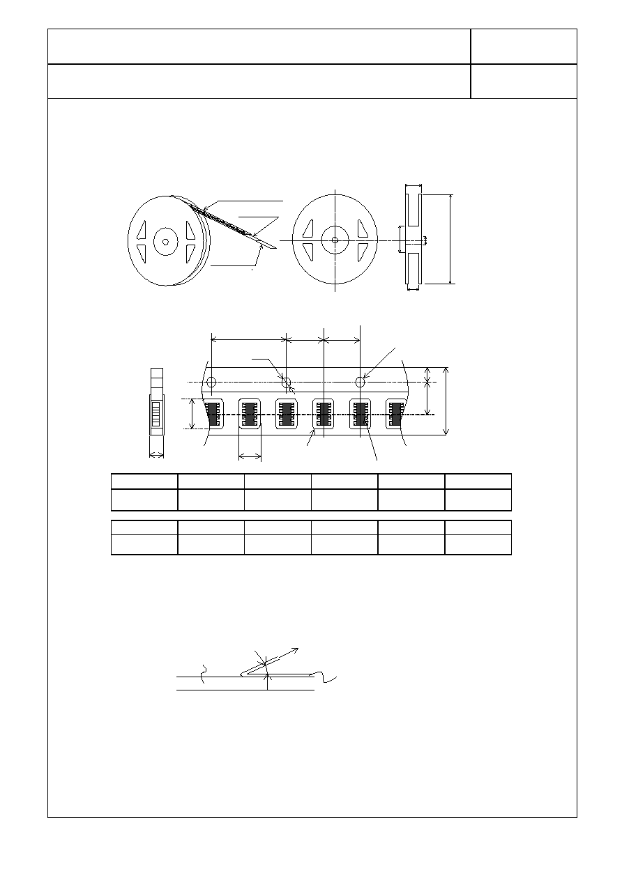
2. Physical Dimensions
2-1. Stracture and reel dimensions shall be as shown in the figure below.
180
11.4
±
1.0
9.0
±
1.0
60m
i
n
.
0 -3
Unit:mm
13.0
±
1.
0
Carrier Tape(Paper)
Top Tape
Adhesive Tape
2-2. Carrier Tape Dimensions
Sprocket hole
Chip hole
P1
P0
P2
A
D0
E
W
F
T
B
Chip resistor array
A
B
W
F
E
(mm)
1.20
±
0.05
2.20
±
0.10
8.00
±
0.20
3.50
±
0.05
1.75
±
0.10
P1
P2
P0
T
D0
(mm)
2.00
±
0.10
2.00
±
0.05
4.00
±
0.10
0.52
±
0.05 1.50
3. Specification
3-1.Taping
When the test shall be operated with the below conditions, peel strength should be 0.049N to
0.49N, should not have flash and tear after peeling.
<Test Method>
∑
Minimum Bending Radius
When carrier tape shall be bent by minimum bending radius (15 mm), no defection of chip and
no break of carrier tape. However minimum bending radius shall be tested for 1 times.
+0.10
0
Peeling Direction
Top Tape
10
∞
Carrier Tape
Subject
Chip Resistor Array PRODUCT SPECIFICATION FOR INFORMATION
Spec. No.
151-EXB-28V02DE
Part No.
EXB28V
EXB28V
EXB28V
EXB28V
9
9
9
9----9999
MATSUSHITA ELECTRONIC COMPONENTS Co.,LTD.
∑
Resistance to climate
When resistors shall be exposed at 60
∞
C
±
2
∞
C, 90 %RH to 95 %RH for 120 hours, no
defection of chip and no break off carrier tape.
When the top tape shall be peeled, tape should not have flash and tear.
3-2. Quantity in Taping: 10,000 pcs. / reel
3-3. Tape packaging
∑
Resistor side shall be facing upward.
∑
Chip resistor shall not be sticking to top tape and bottom tape.
∑
Chip resistors shall be easy to take out from carrier tape and chip hole or sprocket hole shall not
have flash and break.
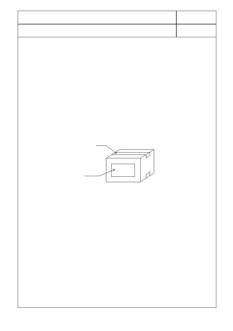
4. Outer Packaging
Quantity: 20reels(Max.200,000 pcs.)
Tape
Marking
∑
When packaging quantity does not reach max quantity, the remaining empty space shall be
buried with buffer material.
∑
When quantity shall be few, alternative packaging methods may used. No problem must occur
during the exportation of the product..
5. Marking
∑
Side of reel(Marking shall be on one side.)
(1)Part name (2)Part number (3)Quantity (4)Lot number (5)Maker name
∑
Packaging box
(1)Customer name (2)Part name (3)Part number (4)Customer part number
(5)Quantity (6)Maker name

Subject
Chip Resistor Array PRODUCT SPECIFICATION FOR INFORMATION
Spec. No.
Attached Sheet
APPEARANCE QUALITY CRITERIA
APPEARANCE QUALITY CRITERIA
APPEARANCE QUALITY CRITERIA
APPEARANCE QUALITY CRITERIA
1
1
1
1----1111
MATSUSHITA ELECTRONIC COMPONENTS Co.,LTD.
Item
Defect Criteria
Appearance Criteria
Remark
Resin Chipping
W
B
C
A
A
W/16
B
C/2
Both side chipping
shall be judged defect
Terminal Chipping
Oblique line show
chipping
A
C
B
D
B
A
C/4
B
Top terminal width
D
3C/4
Pin Hole
One pin hole /
chip resistor
0.2 mm
This item is applied to
pin holes which reach
to the resistive
materials
Flash
A
A
A
100
µ
m