
Stock No. 23123-03 1/01
Preliminary - Subject to Change Without Notice
1
EM128Q16
Preliminary
NanoAmp Solutions, Inc.
1982 Zanker Road, San Jose, CA 95112
ph: 408-573-8878, FAX: 408-573-8877
www.nanoamp.com
EM128Q16 Family
128Kx16 bit Ultra-Low Power Asynchronous Static RAM with Dual Chip Enable
Overview
The EM128Q16 is an integrated memory device
containing a low power 2 Mbit Static Random
Access Memory organized as 131,072 words by 16
bits. The base design is the same as NanoAmp's
EM128V16 but with dual chip enables to reduce
external component count when using two SRAMs
in a system. The device is fabricated using Nano-
Amp's advanced CMOS process and high-speed,
ultra-low-power, low-voltage circuit technology.
These designs are unique in their combination of
fast access time and very low power making them
very suitable for high performance battery powered
applications such as cellular phones and hand held
GPS navigation devices.
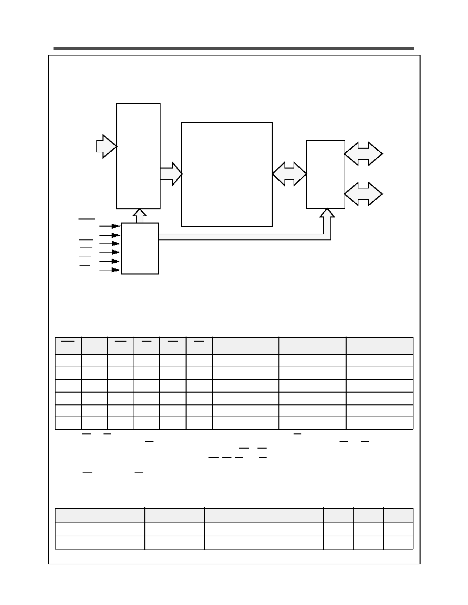
FIGURE 1: Pin Configurations
Features
�
Qualcomm Compatible Voltage Range:
2.3 to 3.0 Volts
�
Dual Chip Enable for Flexible Application
�
Extended Temperature Range:
-40 to +85
o
C
�
Fast Cycle Time:
T
ACC
< 35 ns @ 2.7V
�
Very Low Operating Current:
I
CC
< 1.0 mA typical at 2.5V, 1 Mhz
�
Very Low Standby Current:
I
SB
< 10
�
A
@ 55
o
C
�
44-Pin TSOP, 48-Pin BGA Available
TABLE 1: Pin Descriptions
PIN
ONE
1
2
3
4
5
6
7
8
9
10
11
12
13
14
15
16
17
18
19
20
21
22
A
4
A
3
A
2
A
1
A
0
CE1
I/O
0
I/O
1
I/O
2
I/O
3
VCC
VSS
I/O
4
I/O
5
I/O
6
I/O
7
WE
A
16
A
15
A
14
A
13
A
12
44
43
42
41
40
39
38
37
36
35
34
33
32
31
30
29
28
27
26
25
24
23
A
5
A
6
A
7
OE
U B
L B
I/O
15
I/O
14
I/O
13
I/O
12
VSS
VCC
I/O
11
I/O
10
I/O
9
I/O
8
CE2
A
8
A
9
A
10
A
11
NC
E
M
1
2
8
Q
1
6
T
T
S
O
P
LB
OE
A
0
A
1
A
2
CE2
I/O
8
UB
A
3
A
4
CE1
I/O
0
I/O
9
I/O
10
A
5
A
6
I/O
1
I/O
2
V
SS
I/O
11
NC
A
7
I/O
3
V
CC
V
CC
I/O
12
NC
A
16
I/O
4
V
SS
I/O
14
I/O
13
A
14
A
15
I/O
5
I/O
6
I/O
15
NC
A
12
A
13
WE
I/O
7
NC
A
8
A
9
A
10
A
11
NC
48 Pin BGA (top)
A
B
C
D
E
F
G
H
1 2 3 4 5 6
6 x 8 mm
Pin Name
Pin Function
A
0
-A
16
Address Inputs
WE
Write Enable Input
CE1, CE2
Chip Enable Inputs
OE
Output Enable Input
LB
Lower Byte Enable Input
UB
Upper Byte Enable Input
I/O
0
-I/O
15
Data Inputs/Outputs
NC
Not Connected
V
CC
Power
V
SS
Ground
FIGURE 2: Typical Operating Envelope (R/W Mix)
30
20
10
T
y
p
i
c
a
l
I
C
C
(
m
A
)
10 MHz
1 MHz
V
CC
(V)
5 MHz
0 0.5 1.0 1.5 2.0 2.3 2.5 3.0
0
20 MHz
Specified Operating Range
Stock No. 23123-03 1/01
Preliminary - Subject to Change Without Notice
2
NanoAmp Solutions, Inc.
EM128Q16
Preliminary
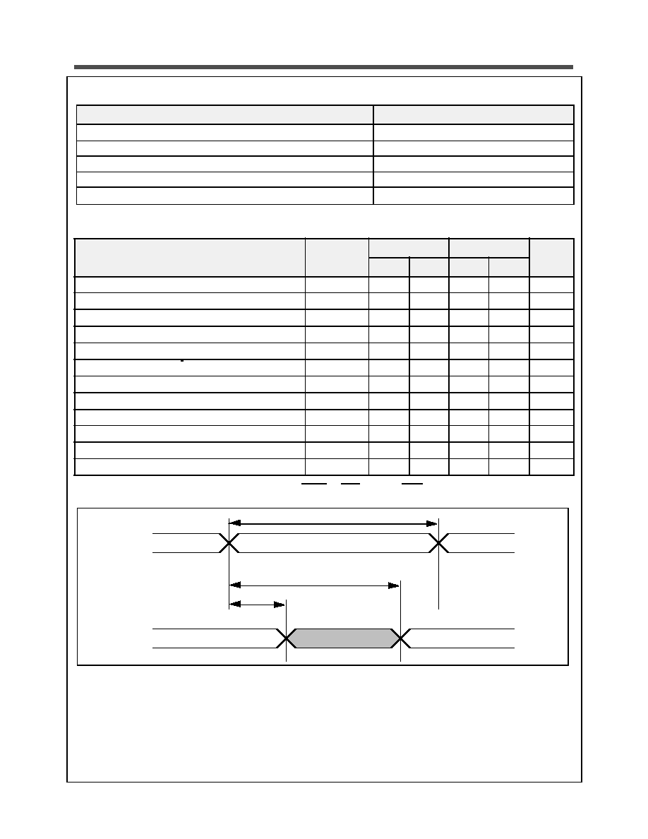
FIGURE 3: Functional Block Diagram
TABLE 2: Functional Description
1. When UB and LB are in select mode (low), I/O
0
- I/O
15
are affected as shown. When LB only is in the select mode only I/O
0
- IO
7
are affected as shown. When UB is in the select mode only I/O
8
- I/O
15
are affected as shown. If both UB and LB are in the dese-
lect mode (high), the chip is active but unaffected by the state of WE or OE.
2. When the device is in standby mode, control inputs (WE, OE, UB, and LB), address inputs and data input/outputs are internally
isolated from any external influence and disabled from exerting any influence externally.
3. When WE is invoked, the OE input is internally disabled and has no effect on the circuit.
4. The device will consume active power in this mode whenever addresses are changed. Data inputs are internally isolated from any
external influence.
TABLE 3: Capacitance*
Note: These parameters are verified in device characterization and are not 100% tested
Control
Logic
Decode
Logic
Address
Inputs
A
0
- A
16
Input/
Output
Mux
and
Buffers
I/O
0
- I/O
7
I/O
8
- I/O
15
Address
128K x 16
Memory
Array
CE1
WE
OE
UB
LB
CE2
CE1
CE2
WE
OE
UB
LB
I/O
0
- I/O
15
1
MODE
POWER
H
X
X
X
X
X
High Z
Standby
2
Standby
X
L
X
X
X
X
High Z
Standby
2
Standby
L
H
X
X
H
H
High Z
Active
Standby
4
L
H
L
X
3
L
1
L
1
Data In
Write
3
Active -> Standby
4
L
H
H
L
L
1
L
1
Data Out
Read
Active -> Standby
4
L
H
H
H
L
1
L
1
High Z
Active
Standby
4
Item
Symbol
Test Condition
Min
Max
Unit
Input Capacitance
C
IN
V
IN
= 0V, f = 1 MHz, T
A
= 25
o
C
8
pF
I/O Capacitance
C
I/O
V
IN
= 0V, f = 1 MHz, T
A
= 25
o
C
8
pF

Stock No. 23123-03 1/01
Preliminary - Subject to Change Without Notice
3
NanoAmp Solutions, Inc.
EM128Q16
Preliminary
TABLE 4: Absolute Maximum Ratings*
* Stresses greater than those listed above may cause permanent damage to the device. This is a stress rating only and functional
operation of the device at these or any other conditions above those indicated in the operating section of this specification is not
implied. Exposure to absolute maximum rating conditions for extended periods may affect reliability.
TABLE 5: Operating Characteristics (Over specified Temperature Range)
1. Operating current is a linear function of operating frequency and voltage. You may calculate operating current using the formul a
shown with operating frequency (f) expressed in MHz and operating voltage (V) in volts. Example: When operating at 2 MHz at
2.0 volts the device will draw a typical active current of 0.8*2*2 = 3.2 mA in the page access mode. This parameter is specified
with the outputs disabled to avoid external loading effects. The user must add current required to drive output capacitance
expected in the actual system.
2. This device assumes a standby mode if the chip is disabled (CE1 high or CE2 low). It will also automatically go into a standby
mode whenever all input signals are quiescent (not toggling) regardless of the state of CE1 or CE2. In order to achieve low
standby current all inputs must be within 0.2 volts of either VCC or VSS.
3. The Chip is Disabled when CE1 is high or CE2 is low. The Chip is Enabled when CE1 is low and CE2 is high.
Item
Symbol
Rating
Unit
Voltage on any pin relative to V
SS
V
IN,OUT
-0.3 to V
CC
+0.3
V
Voltage on V
CC
Supply Relative to V
SS
V
CC
-0.3 to 4.0
V
Power Dissipation
P
D
500
mW
Storage Temperature
T
STG
-40 to 125
o
C
Operating Temperature
T
A
-40 to +85
o
C
Soldering Temperature and Time
T
SOLDER
260
o
C, 10sec(Lead only)
o
C
Item
Symbol
Test Conditions
Min
Typ
Max
Unit
Supply Voltage
V
CC
2.3
3.0
V
Data Retention Voltage
V
DR
Chip Disabled (Note 3)
1.2
V
Input High Voltage
V
IH
0.7V
CC
V
CC
+0.5
V
Input Low Voltage
V
IL
�0.5
0.3V
CC
V
Output High Voltage
V
OH
I
OH
= 0.2mA
V
CC
�0.3
V
Output Low Voltage
V
OL
I
OL
= -0.2mA
0.3
V
Input Leakage Current
I
LI
V
IN
= 0 to V
CC
0.5
�
A
Output Leakage Current
I
LO
OE = V
IH
or Chip Disabled
0.5
�
A
Read/Write Operating Supply Cur-
rent (Note 1)
I
CC1
V
IN
= V
IH
or V
IL
Chip Enabled, Iout = 0
0.5fV
mA
Read/Write Quiescent Operating
Supply Current (Note 2)
I
CC3
V
IN
= V
CC
or 0V
Chip Enabled, Iout = 0
f = 0, t
A
= 55
o
C
10
�
A
Operating Standby Current @ 55
o
C
(Note 2)
I
SB1
V
IN
= V
CC
or 0V
Chip Disabled, t
A
= 55
o
C
10
�
A
Operating Standby Current @ 85
o
C
(Note 2)
I
SB1
V
IN
= V
CC
or 0V
Chip Disabled, t
A
= 85
o
C
40
�
A
Maximum Data Retention Current
(Note 2)
I
DR
Vcc = 1.2V, V
IN
= V
CC
or 0
Chip Disabled, t
A
= 55
o
C
1
�
A
Stock No. 23123-03 1/01
Preliminary - Subject to Change Without Notice
4
NanoAmp Solutions, Inc.
EM128Q16
Preliminary
TABLE 6: Timing Test Conditions
TABLE 7: Read Cycle Timing
FIGURE 4: Timing of Read Cycle (1) (CE1 = OE = V
IL
, WE = CE2 = V
IH
)
Item
Input Pulse Level
0.1V
CC
to 0.9 V
CC
Input Rise and Fall Time
5ns
Input and Output Timing Reference Levels
0.5 V
CC
Output Load
CL = 30pF
Operating Temperature
-40 to +85
o
C
Item
Symbol
2.3 - 3.0 V
2.7 - 3.0 V
Units
Min.
Max.
Min.
Max.
Read Cycle Time
t
RC
55
35
ns
Address Access Time
t
AA
55
35
ns
Chip Enable to Valid Output
t
CO
55
35
ns
Output Enable to Valid Output
t
OE
20
15
ns
Byte Select to Valid Output
t
LB
, t
UB
20
15
ns
Chip Enable to Low-Z output
t
LZ
5
5
ns
Output Enable to Low-Z Output
t
OLZ
3
3
ns
Byte Select to Low-Z Output
t
LBZ
, t
UBZ
5
5
ns
Chip Enable to High-Z Output
t
HZ
5
15
5
15
ns
Output Disable to High-Z Output
t
OHZ
5
15
5
15
ns
Byte Select Disable to High-Z Output
t
LBHZ
, t
UBHZ
5
15
5
15
ns
Output Hold from Address Change
t
OH
5
5
ns
Address
Data Out
t
RC
t
AA
t
OH
Data Valid
Previous Data Valid

Stock No. 23123-03 1/01
Preliminary - Subject to Change Without Notice
5
NanoAmp Solutions, Inc.
EM128Q16
Preliminary
FIGURE 5: Timing Waveform of Read Cycle (2) (WE = V
IH
)
TABLE 8: Write Cycle Timing
Item
Symbol
2.3 - 3.0 V
2.7 - 3.0 V
Units
Min.
Max.
Min.
Max.
Write Cycle Time
t
WC
55
35
ns
Chip Enable to End of Write
t
CW
30
25
ns
Address Valid to End of Write
t
AW
30
25
ns
Byte Select to End of Write
t
LBW
, t
UBW
30
25
ns
Address Set-up Time
t
AS
0
0
ns
Write Pulse Width
t
WP
30
25
ns
Write Recovery Time
t
WR
0
0
ns
Write to High-Z Output
t
WHZ
15
10
ns
Data to Write Time Overlap
t
DW
20
15
ns
Data Hold from Write Time
t
DH
0
0
ns
End Write to Low-Z Output
t
OW
5
5
ns
Address
LB, UB
OE
Data Valid
t
RC
t
AA
t
CO
t
HZ(1,2)
t
OHZ(1)
t
LBHZ,
t
UBHZ
t
OLZ
t
OE
t
LZ(2)
High-Z
Data Out
t
LB,
t
UB
t
LBLZ,
t
UBLZ
CE1
CE2