1
Stock No. 23184-B 5/03
NanoAmp Solutions, Inc.
1982 Zanker Road, San Jose, CA 95112
ph: 408-573-8878, FAX: 408-573-8877
www.nanoamp.com
N36N183WPFA
N36N363WPFA
N36N723WPFA
Advance Information
This is an advance datasheet and subject to change without notice.
NanoAmp Proprietary and Confidential
FtRAM is a trademark of NanoAmp Solutions, Inc.
NoBL is a trademark of Cycpress Semiconductor Corpopation
ZBT is a trademark of Integrated Device Technology
NtRAM is a trademark of Samsung Electronics Corporation
36Mb High Speed Synchronous SRAMs with Fast Bus Turn-around
TM
FTRAM
TM
Architecture
Features
∑
High performance synchronous operation
∑
Cycle times up to 300MHz
Access times as fast as 2.3nS
∑
Full 100% bus utilization
∑
Fully compatible with other no bus turn-
around SRAMs
∑
Single device supports power supply of
3.3V or 2.5V
∑
Separate I/O power supply of 3.3V or 2.5V
∑
User selectable pipeline and flow-thru oper-
ating modes for BGA devices
∑
Individual byte write operation
∑
Three chip enables
Simple depth expansion
∑
ZZ mode for low power sleep mode
∑
Mode pin for setting interleave or linear
burst mode of operation
∑
JTAG Boundary Scan (BGA only)
∑
JEDEC standard packages: 100-pin TQFP,
165-ball FPBGA, 119-ball PBGA and 209-
ball PBGA (x72)
Functional Description
These 36Mb high performance synchronous
SRAMs form a family of device options for those
demanding high performance. The FTRAM
TM
fam-
ily of devices is designed to operate without the
need of NOP or deselect clock cycles when transi-
tioning from read to write cycles and thereby allow-
ing the use of all available bandwidth. The high
speed devices are fully compatible with other no
bus turn-around SRAMs such as NoBL
TM
, ZBT
TM
and NtRAM
TM
devices.
The memory devices contain 36Mb of memory
cells organized as 2,097,152 x 18 (N36N18),
1,048,576 x 36 (N36N36) and 524,288 x 72
(N36N72). The devices operate in a synchronous
manner with control signals, addresses and data
inputs synchronized and captured at the rising
edge of clock for ease of use. An asynchronous
OE is available for disabling the outputs at any
time. An asynchronous ZZ signal can be used to
put the device into sleep mode with all data
retained. User configurable operation in pipeline or
flow-thru modes is allowed through control of the
FT input for BGA devices. Either pipeline or flow-
thru devices are available in TQFP packages. The
devices are fabricated using NanoAmp's advanced
CMOS process and high-speed/ultra low-power
circuit technology.
This 36Mb family is ideal for networking and com-
munication systems where high-density, high-per-
formance memory elements are required. The
architecture allows the data bus to be fully utilized
when moving data into and out of the SRAM.
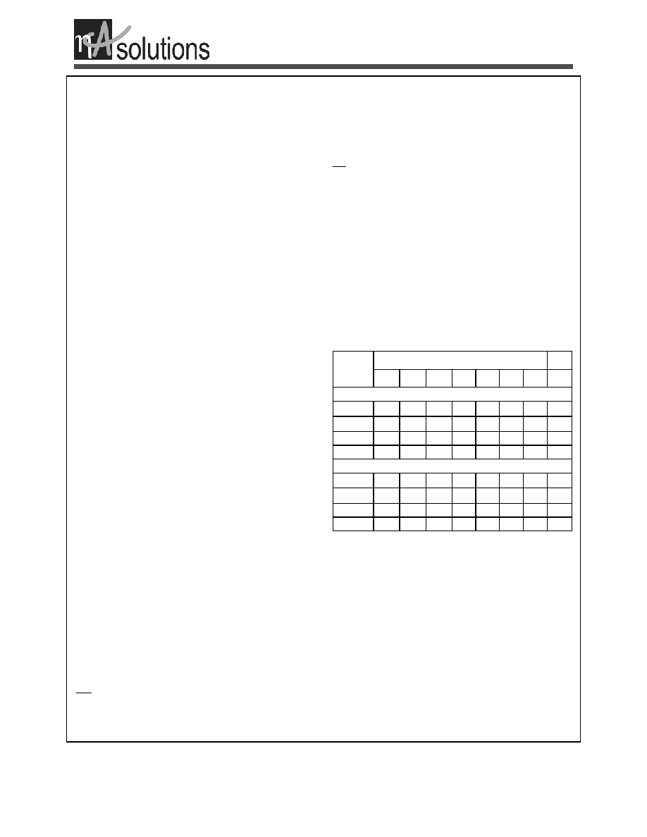
Performance and Power examples for
P1 and PF devices
SORT
-13
-15
-16
-20
-22
-25
-30
Unit
In Pipeline Mode
t
CYCLE
7.5
6.7
6.0
5.0
4.4
4.0
3.3
nS
t
ACCESS
4.0
3.8
3.5
3.0
2.8
2.7
2.3
nS
Icc
200
220
250
300
310
320
tbd
mA
Isb
20
20
20
20
20
20
20
mA
In Flow-Thru Mode
t
CYCLE
15.0
10.0 10.0
8.5
7.5
6.7
nS
t
ACCESS
11.0
10.0 8.5
7.0
6.5
6.0
nS
Icc
110
120
130
150
200
220
mA
Isb
20
20
20
20
20
20
mA
Options
∑
Organization
2Mb x 18
N36N183W
1Mb x 36
N36N363W
512Kb x 72
N36N723W
∑
Operating Mode
P1 (only for TQFP)
Pipeline
F1 (only for TQFP)
Flow-Thru
PF (for all BGA)
Pipeline or Flow-Thru
∑
Package
100-pin TQFP
Q
119-ball PBGA
G
165-ball FPBGA
F
209-ball PBGA
X

NanoAmp Solutions
2
Stock No. 23184-B 5/03
This is an advance datasheet and subject to change without notice.
NanoAmp Proprietary and Confidential
N36N183WPFA
N36N363WPFA
N36N723WPFA
Advance Information
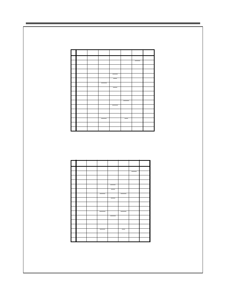
100-Pin TQFP Packages
(2M x 18)
NC
NC
NC
VDDQ
VSS
NC
NC
DQb
DQb
VSS
VDDQ
DQb
DQb
NC
VDD
NC
VSS
DQb
DQb
VDDQ
VSS
DQb
DQb
DQbP
NC
VSS
VDDQ
NC
NC
NC
A
NC
NC
VDDQ
VSS
NC
DQaP
DQa
DQa
VSS
VDDQ
DQa
DQa
VSS
NC
VDD
ZZ
DQa
DQa
VDDQ
VSS
DQa
DQa
NC
NC
VSS
VDDQ
NC
NC
NC
A
A
CE1
CE2
NC
NC
BWb
BW
a
CE3
VDD
VSS
CLK
WE
CEN
OE
ADV
A
A
A
A
LB
O
A
A
A
A
A1
A0
NC
NC
VS
S
VD
D
NC
A
A
A
A
A
A
A
A
1
2
3
4
5
6
7
8
9
10
11
12
13
14
15
16
17
18
19
20
21
22
23
24
25
26
27
28
29
30
31
32
33
34
35
36
37
38
39
40
41
42
43
44
45
46
47
48
49
50
80
79
78
77
76
75
74
73
72
71
70
69
68
67
66
65
64
63
62
61
60
59
58
57
56
55
54
53
52
51
10
0
99
98
97
96
95
94
93
92
91
90
89
88
87
86
85
84
83
82
81
(1M x 36)
1
2
3
4
5
6
7
8
9
10
11
12
13
14
15
16
17
18
19
20
21
22
23
24
25
26
27
28
29
30
31
32
33
34
35
36
37
38
39
40
41
42
43
44
45
46
47
48
49
50
80
79
78
77
76
75
74
73
72
71
70
69
68
67
66
65
64
63
62
61
60
59
58
57
56
55
54
53
52
51
DQcP
DQc
DQc
VDDQ
VSS
DQc
DQc
DQc
DQc
VSS
VDDQ
DQc
DQc
NC
VDD
NC
VSS
DQd
DQd
VDDQ
VSS
DQd
DQd
DQd
DQd
VSS
VDDQ
DQd
DQd
DQdP
DQbP
DQb
DQb
VDDQ
VSS
DQb
DQb
DQb
DQb
VSS
VDDQ
DQb
DQb
VSS
NC
VDD
ZZ
DQa
DQa
VDDQ
VSS
DQa
DQa
DQa
DQa
VSS
VDDQ
DQa
DQa
DQaP
A
A
CE1
CE2
BWd
BWc
BWb
BW
a
CE3
VDD
VS
S
CLK
WE
CEN
OE
ADV
A
A
A
A
LBO
A
A
A
A
A1
A0
DNU
DNU
VSS
VDD
DNU
A
A
A
A
A
A
A
A
10
0
99
98
97
96
95
94
93
92
91
90
89
88
87
86
85
84
83
82
81