Document No. D14858EJ2V0DS00 (2nd edition)
Date Published April 2002 N CP(K)
Printed in Japan
SILICON POWER TRANSISTOR
2SA1742
PNP SILICON EPITAXIAL TRANSISTOR
FOR HIGH-SPEED SWITCHING
DATA SHEET
The information in this document is subject to change without notice. Before using this document, please
confirm that this is the latest version.
Not all devices/types available in every country. Please check with local NEC representative for
availability and additional information.
©
2002
The 2SA1742 is a power transistor developed for high-speed
switching and features a high h
FE
at low V
CE(sat)
. This transistor is ideal
for use as a driver in DC/DC converters and actuators.
In addition, a small resin-molded insulation type package
contributes to high-density mounting and reduction of mounting cost.
FEATURES
∑ High h
FE
and low V
CE(sat)
:
h
FE
100 MIN. @V
CE
=
-2.0 V, I
C
=
-1.5 A
V
CE(sat)
-0.3 V MAX. @I
C
=
-4.0 V, I
B
=
-0.2 A
∑ Full-mold package that does not require an insulating board or
bushing
ABSOLUTE MAXIMUM RATINGS (T
A
= 25
∞
∞
∞
∞C)
Parameter
Symbol
Conditions
Ratings
Unit
Collector to base voltage
V
CBO
-100
V
Collector to emitter voltage
V
CEO
-60
V
Emitter to base voltage
V
EBO
-7.0
V
Collector current (DC)
I
C(DC)
-7.0
A
Collector current (pulse)
I
C(pulse)
PW
300
µs,
duty cycle
10%
-14
A
Base current (DC)
I
B(DC)
-3.5
A
T
C
= 25
∞C
30
W
Total power dissipation
P
T
T
A
= 25
∞C
2.0
W
Junction temperature
T
j
150
∞C
Storage temperature
T
stg
-55 to +150
∞C
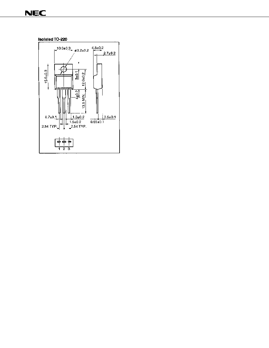
ORDERING INFORMATION
Part No.
Package
2SA1742
Isolated TO-220
(Isolated TO-220)
Data Sheet D14858EJ2V0DS
2
2SA1742
ELECTRICAL CHARACTERISTICS (T
A
= 25
∞
∞
∞
∞C)
Parameter
Symbol
Conditions
MIN.
TYP.
MAX.
Unit
V
CEO(SUS)
I
C
=
-4.0 V, I
B
=
-0.4 A, L = 1 mH
-60
V
Collector to emitter voltage
V
CEX(SUS)
I
C
=
-4.0 A, I
B1
=
-I
B2
=
-0.4 A,
V
BE(OFF)
= 1.5 V, L = 180
µH, clamped
-60
V
I
CBO
V
CB
=
-60 V, I
E
= 0 A
-10
µA
I
CER
V
CE
=
-60 V, R
BE
= 50
, T
A
= 125
∞C
-1.0
mA
I
CEX1
V
CE
=
-60 V, V
BE(OFF)
= 1.5 V
-10
µA
Collector cutoff current
I
CEX2
V
CE
=
-60 V, V
BE(OFF)
= 1.5 V,
T
A
= 125
∞C
-1.0
mA
Emitter cutoff current
I
EBO
V
EB
=
-5.0 V, I
C
= 0 A
-10
µA
h
FE1
V
CE
=
-2.0 V, I
C
=
-0.7 A
Note
100
h
FE2
V
CE
=
-2.0 V, I
C
=
-1.5 A
Note
100
400
DC current gain
h
FE3
V
CE
=
-2.0 V, I
C
=
-4.0 A
Note
60
V
CE(sat)1
I
C
=
-4.0 A, I
B
=
-0.2 A
Note
-0.3
V
Collector saturation voltage
V
CE(sat)2
I
C
=
-6.0 A, I
B
=
-0.3 A
Note
-0.5
V
V
BE(sat)1
I
C
=
-4.0 A, I
B
=
-0.2 A
Note
-1.2
V
Base saturation voltage
V
BE(sat)2
I
C
=
-6.0 A, I
B
=
-0.3 A
Note
-1.5
V
Collector capacitance
C
ob
V
CB
=
-10 V, I
E
= 0 A, f = 1.0 MHz
180
pF
Gain bandwidth product
f
T
V
CB
=
-10 V, I
C
=
-1.0 A
40
MHz
Turn-on time
t
on
0.3
µs
Storage time
t
stg
1.5
µs
Fall time
t
f
I
C
=
-4.0 A, R
L
= 12.5
,
I
B1
=
-I
B2
=
-0.2 A, V
CC
-50 V
Refer to the test circuit.
0.3
µs
Note Pulse test PW
350
µs, duty cycle 2%
h
FE
CLASSIFICATION
Marking
M
L
K
h
FE2
100 to 200
150 to 300
200 to 400
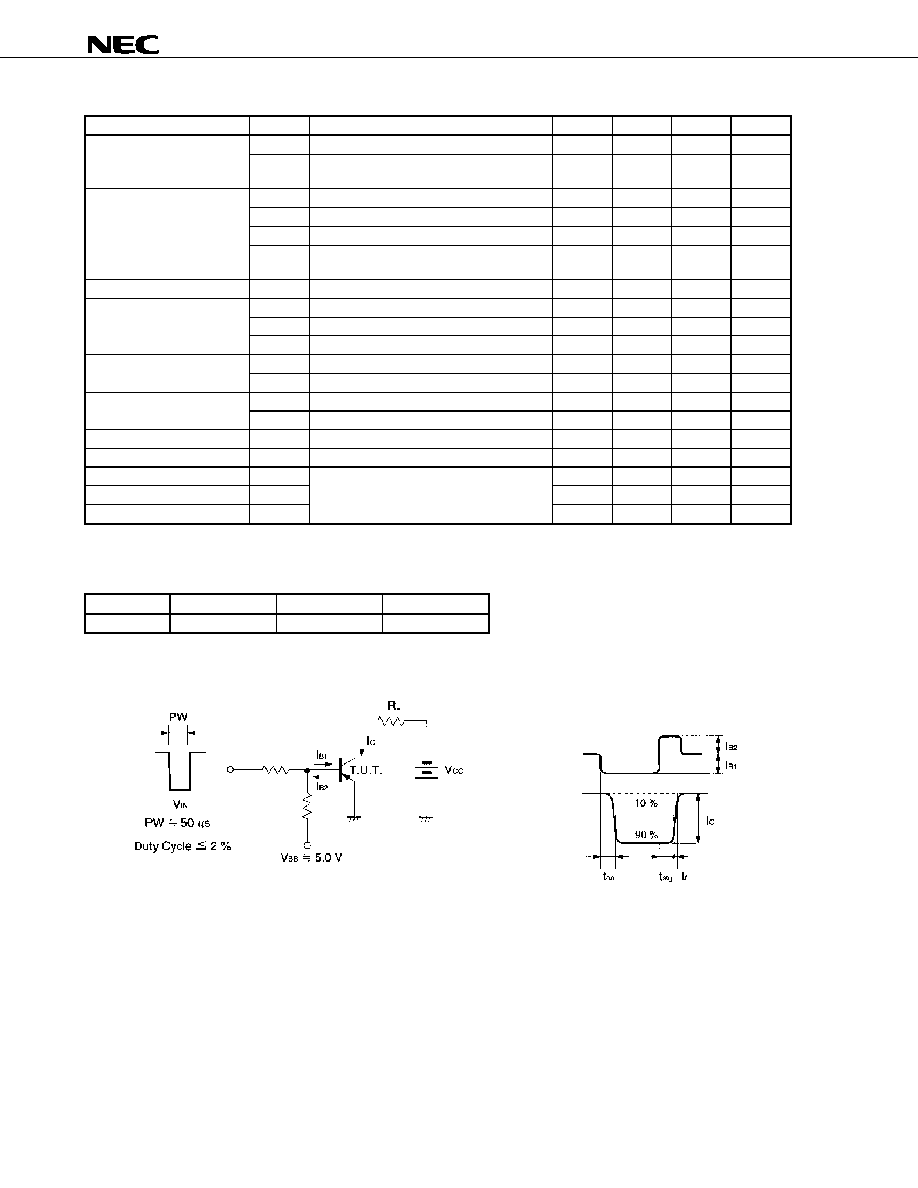
SWITCHING TIME (t
on
, t
stg
, t
f
) TEST CIRCUIT
Base current
waveform
Collector current
waveform

Data Sheet D14858EJ2V0DS
3
2SA1742
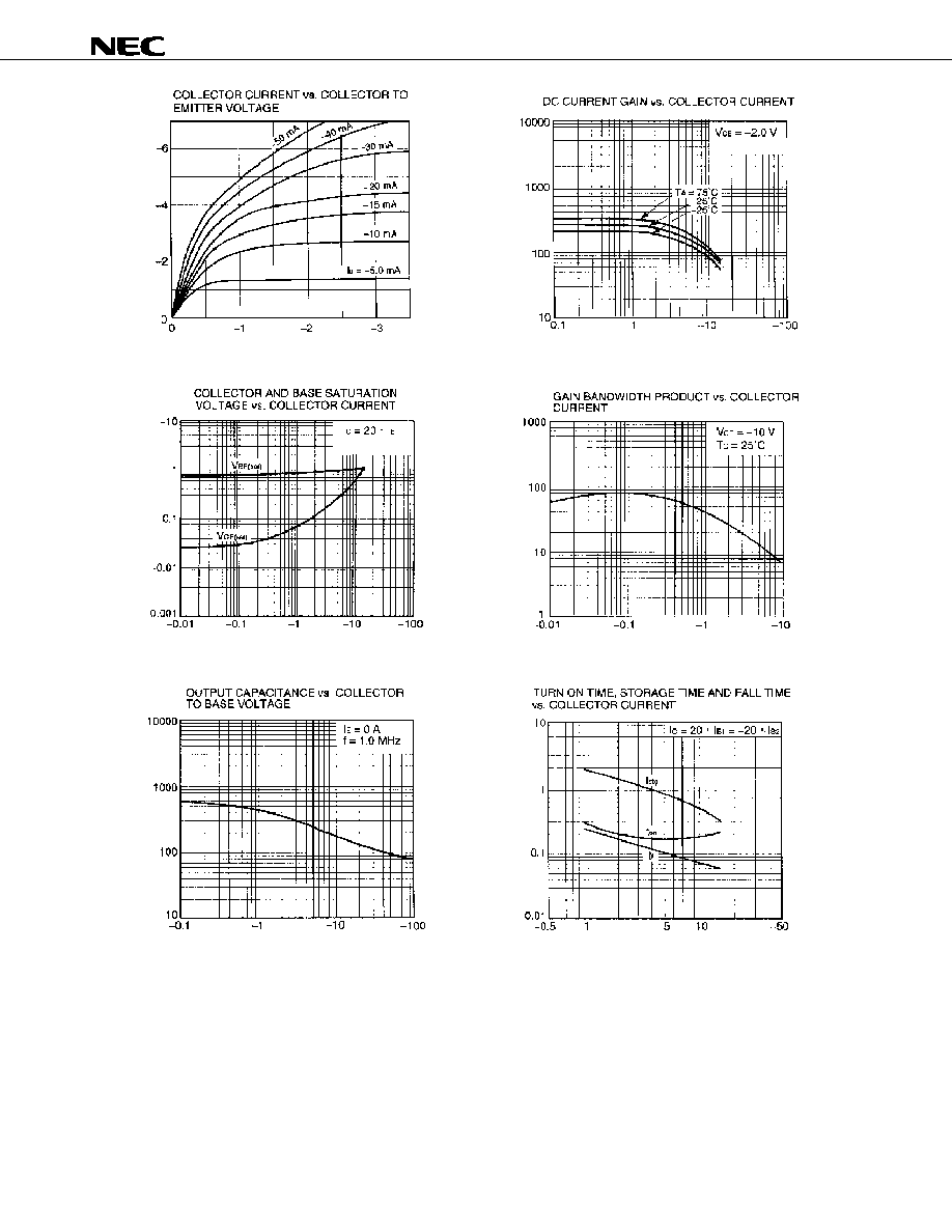
TYPICAL CHARACTERISTICS (T
A
= 25
∞
∞
∞
∞C)
T
o
t
a
l
P
o
w
e
r
Di
s
s
i
pa
t
i
on
P
T
(W)
Case Temperature T
C
(
∞C)
Collector to Emitter Voltage V
CE
(V)
Case Temperature T
C
(
∞C)
Derat
i
ng dT
(
%
)
Trans
i
ent
Therm
a
l
Res
i
s
t
an
c
e
r
th
(
t
)
(
∞
C/
W
)
Collector to Emitter Voltage V
CE
(V)
Pulse Width PW (s)
Col
l
e
c
t
or Current
I
C
(
A
)
Col
l
e
c
t
or Current
I
C
(
A
)
Single pulse
Col
l
e
c
t
or c
u
rrent
I
C
(
A
)
Without heatsink
With infinite heatsink