
The information in this document is subject to change without notice. Before using this document, please
confirm that this is the latest version.
Not all devices/types available in every country. Please check with local NEC representative for
availability and additional information.
1998
©
Document No. D16135EJ2V0DS00 (2nd edition)
Date Published April 2002 N CP(K)
Printed in Japan
SILICON TRANSISTORS
2SC2885, 2946, 2946(1)
NPN SILICON
EPITAXIAL TRANSISTOR
FOR HIGH-VOLTAGE HIGH-SPEED SWITCHING
DATA SHEET
2002
The 2SC2885, 2946, and 2946(1) are high-voltage high-speed switching power transistors featuring a small
package (MP-3) which is suitable for high-density mounting. These transistors are ideal for drivers in DC/DC
converters and switching regulators.
There are three types of transistors selectable according to the reliability requirments: 2SC2946 and 2946(1) for
industrial use, 2SC2885 for general use. The 2SC2946(1) is produced with leads so as to enable mounting directly in
a hybrid IC.
QUALITY GRADES
∑ Standard
Please refer to "Quality Grades on NEC Semiconductor Devices" (Document No. C11531E) published by NEC
Corporation to know the specification of quality grade on the devices and its recommended applications.
ABSOLUTE MAXIMUM RATINGS (Ta = 25
∞
∞
∞
∞C)
Parameter
Symbol
Ratings
Unit
Collector to base voltage
V
CBO
330
V
Collector to emitter voltage
V
CEO
200
V
Emitter to base voltage
V
EBO
7.0
V
Collector current (DC)
I
C(DC)
2.0
A
Collector current (pulse)
I
C(pulse)
*
4.0
A
Base current (DC)
I
B(DC)
1.0
A
Total power dissipation
P
T
(Tc = 25
∞C)
15
W
Total power dissipation
P
T
(Ta = 25
∞C)
600
mW
Junction temperature
T
j
150
∞C
Storage temperature
T
stg
-55 to +150
∞C
* PW
300
µs, duty cycle 10%
Data Sheet D16135EJ2V0DS
2
2SC2885, 2946, 2946(1)
ELECTRICAL CHARACTERISTICS (Ta = 25
∞
∞
∞
∞C)
Parameter
Symbol
Conditions
MIN.
TYP.
MAX.
Unit
Collector to emitter voltage
V
CEO(SUS)
I
C
= 1.0 A, I
B
= 0.1 A, L = 500
µH*
200
V
Collector to emitter voltage
V
CEX(SUS)
I
C
= 1.0 A, I
B1
=
-I
B2
= 0.1 A*
Ta = 125
∞C, L = 180
µH, clamped
200
V
Collector cutoff current
I
CBO
V
CB
= 250 V, I
E
= 0
10
µA
Collector cutoff current
I
CEX1
V
CE
= 250 V, V
BE(OFF)
=
-1.5 V
10
µA
Collector cutoff current
I
CEX2
V
CE
= 250 V, V
BE(OFF)
=
-1.5 V, Ta = 125∞C
1.0
mA
Emitter cutoff current
I
EBO
V
EB
= 5.0 V, I
C
= 0
1.0
µA
h
FE1
V
CE
= 5.0 V, I
C
= 0.1 A*
20
60
160
DC current gain
h
FE2
V
CE
= 5.0 V, I
C
= 1.0 A*
15
Collector saturation voltage
V
CE(sat)
I
C
= 1.0 A, I
B
= 0.1 A*
1.0
V
Base saturation voltage
V
BE(sat)
I
C
= 1.0 A, I
B
= 0.1 A*
1.5
V
Turn-on time
t
on
1.0
µs
Storage time
t
stg
2.0
µs
Fall time
t
f
I
C
= 1.0 A, R
L
= 100
I
B1
=
-I
B2
= 0.1 A, V
CC
100 V
Refer to the test circuit.
1.0
µs
* Pulse test PW
350
µs, duty cycle 2%
h
FE
CLASSIFICATION
Marking
N
M
L
K
h
FE1
20 to 50
30 to 70
50 to 100
80 to 160
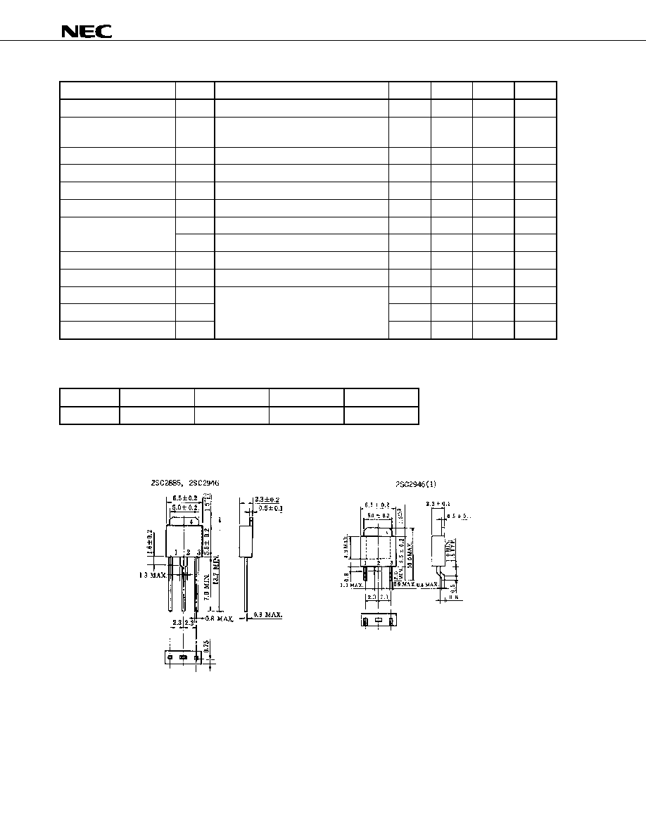
PACKAGE DRAWING (UNIT: mm)
Electrode Connection
1. Base
2. Collector
3. Emitter
4. Collector (fin)

Data Sheet D16135EJ2V0DS
3
2SC2885, 2946, 2946(1)
TYPICAL CHARACTERISTICS (Ta = 25
∞
∞
∞
∞C)
T
o
ta
l
P
o
we
r
Dis
s
i
p
a
ti
o
n
P
T
(W
)
Ambient Temperature T
a
(
∞
C)
Case Temperature T
C
(
∞
C)
Collector to Emitter Voltage V
CE
(V)
Co
l
l
e
c
to
r
Cu
r
r
e
n
t
I
C
(
m
A)
Co
l
l
e
c
to
r
Cu
r
r
e
n
t
I
C
(
A
)
Pulse Width PW (ms)
Collector to Emitter Voltage V
CE
(V)
Collector Current I
C
(mA)
???
Tr
ans
i
e
nt
Ther
m
a
l
R
e
s
i
s
t
anc
e R
t
h
(j
-a
)
(
∞
C/
W
)
DC Cu
rr
e
n
t Ga
i
n
h
FE
I
C
De
r
a
ti
n
g
d
T
(%
)
Pulse test
Without
heatsink
W
i
th i
n
fi
n
i
te
heat
s
i
n
k

