 | –≠–ª–µ–∫—Ç—Ä–æ–Ω–Ω—ã–π –∫–æ–º–ø–æ–Ω–µ–Ω—Ç: 2SC4095 | –°–∫–∞—á–∞—Ç—å:  PDF PDF  ZIP ZIP |
DATA SHEET
SILICON TRANSISTOR
2SC4095
MICROWAVE LOW NOISE AMPLIFIER
NPN SILICON EPITAXIAL TRANSISTOR
4 PINS MINI MOLD
DATA SHEET
Document No. P10367EJ2V1DS00 (2nd edition)
Date Published March 1997 N
Printed in Japan
1987
©
DESCRIPTION
The 2SC4095 is an NPN epitaxial silicon transistor designed for use in
low-noise and small signal amplifiers from VHF band to UHF band.
2SC4095 features excellent power gain with very low-noise figures.
2SC4095 employs direct nitiride passivated base surface process (DNP
process) which is an NEC proprietary new fabrication technique which
provides excellent noise figures at high current values. This allows
excellent associated gain and very wide dynamic range.
FEATURES
∑ NF = 1.8 dB TYP. @ f = 2.0 GHz, V
CE
= 6 V, I
C
= 5 mA
∑
S
21e
2
= 9.5 dB TYP. @ f = 2.0 GHz, V
CE
= 6 V, I
C
= 10 mA
ABSOLUTE MAXIMUM RATINGS (T
A
= 25
C)
Collector to Base Voltage
V
CBO
20
V
Collector to Emitter Voltage
V
CEO
10
V
Emitter to Base Voltage
V
EBO
1.5
V
Collector Current
I
C
35
mA
Total Power Dissipation
P
T
200
mW
Junction Temperature
T
j
150
C
Storage Temperature
T
stg
65 to +150
C
ELECTRICAL CHARACTERISTICS (T
A
= 25
C)
CHARACTERISTIC
SYMBOL
MIN.
TYP.
MAX.
UNIT
TEST CONDITIONS
Collector Cutoff Current
I
CBO
1.0
A
V
CB
= 10 V, I
E
= 0
Emitter Cutoff Current
I
EBO
1.0
A
V
EB
= 1 V, I
C
= 0
DC Current Gain
h
FE
50
100
250
V
CE
= 6 V, I
C
= 10 mA
Gain Bandwidth Product
f
T
10
GHz
V
CE
= 6 V, I
C
= 10 mA f = 1.0 GHz
Feed-Back Capacitance
C
re
0.25
0.8
pF
V
CB
= 10 V, I
E
= 0, f = 1.0 MHz
Insertion Power Gain
S
21e
2
7.5
9.5
dB
V
CE
= 6 V, I
C
= 10 mA, f = 2.0 GHz
Maximum Available Gain
MAG
12
dB
V
CE
= 6 V, I
C
= 10 mA, f = 2.0 GHz
Noise Figure
NF
1.8
3.0
dB
V
CE
= 6 V, I
C
= 5 mA, f = 2.0 GHz
h
FE
Classification
Class
R46/RDF *
R47/RDG *
R48/RDH *
Marking
R46
R47
R48
h
FE
50 to 100
80 to 160
125 to 250
* Old Specification / New Specification
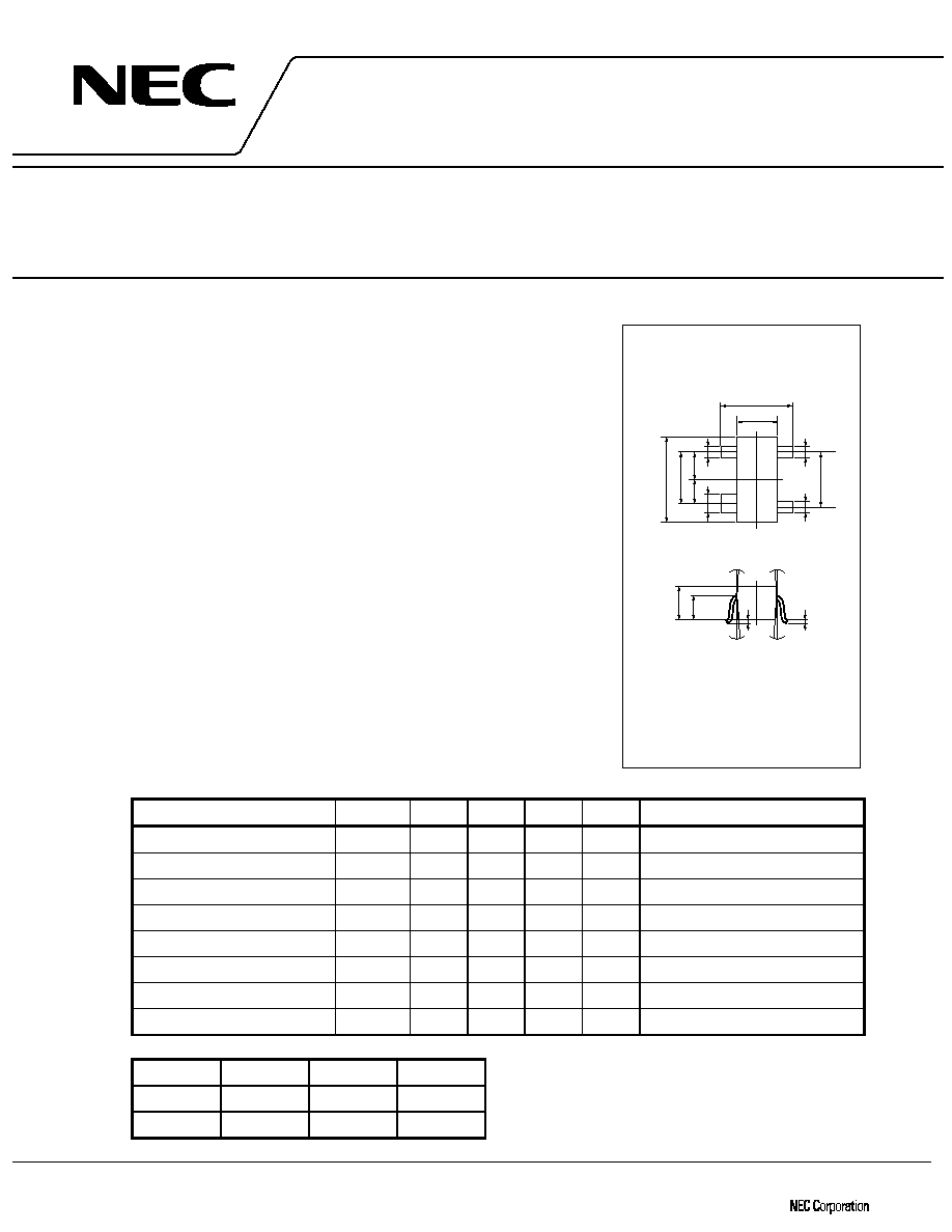
PACKAGE DIMENSIONS
(Units: mm)
PIN CONNECTIONS
1.
2.
3.
4.
Collector
Emitter
Base
Emitter
5
∞
5
∞
5
∞
5
∞
0 to 0.1
0.8
2.9±0.2
(1.8)
(1.9)
0.95
0.85
1.1
+0.2
-
0.1
0.16
+0.1
-
0.06
0.4
4
1
3
2
+0.1
-
0.05
2.8
+0.2
-
0.3
1.5
+0.2
-
0.1
0.6
+0.1
-
0.05
0.4
+0.1
-
0.05
0.4
+0.1
-
0.05
2
2SC4095
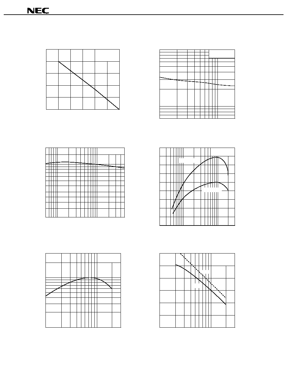
TYPICAL CHARACTERISTICS (T
A
= 25
C)
TOTAL POWER DISSIPATION vs.
AMBIENT TEMPERATURE
200
100
0
10
20
50
100
200
50
1
5
10
50
0.5
100
150
T
A
-Ambient Temperature-
∞
C
I
C
-Collector Current-mA
DC CURRENT GAIN vs.
COLLECTOR CURRENT
P
T
-Total Power Dissipation-mW
h
FE
-DC Current Gain
V
CE
= 6 V
I
C
-Collector Current-mA
INSERTION GAIN vs.
COLLECTOR CURRENT
|S
21e
|
2
-Insertion Gain-dB
0.06
0.2
0.1
1
1.0
1
2
5
10
20
V
CB
-Collector to Base Voltage-V
FEED-BACK CAPACITANCE vs.
COLLECTOR TO BASE VOLTAGE
C
re
-Feed-back Capacitance-pF
f = 1.0 GHz
0
2
4
6
10
12
14
16
18
8
0.2
1
0.5
2
5
10
20 30
0
10
20
30
0.1
0.2
0.5
1.0
2.0
3.0
f-Frequency-GHz
MAXIMUM AVAILABLE GAIN, INSERTION
GAIN vs. FREQUENCY
|S
21e
|
2
-Insetion Gain -dB
MAG-Maximum Available Gain-dB
V
CE
= 6 V
f
C
= 10 mA
5
2
10
30
20
1
2
5
10
20
30
I
C
-Collector Current-mA
GAIN BANDWIDTH PRODUUT vs.
COLLECTOR CURRENT
f
T
-Gain Bandwidth Product-MHz
V
CE
= 6 V
Free Air
|S
21e
|
2
MAG
V
CE
= 6 V
f = 1.0 GHz
f = 2.0 GHz
0.5

3
2SC4095
0
2
1
5
4
3
7
6
0.5
1
5
10
50 70
I
C
-Collector Current-mA
NOISE FIGURE vs.
COLLECTOR CURRENT
NF-Noise Figure-dB
V
CE
= 10 V
f = 2.0 GHz
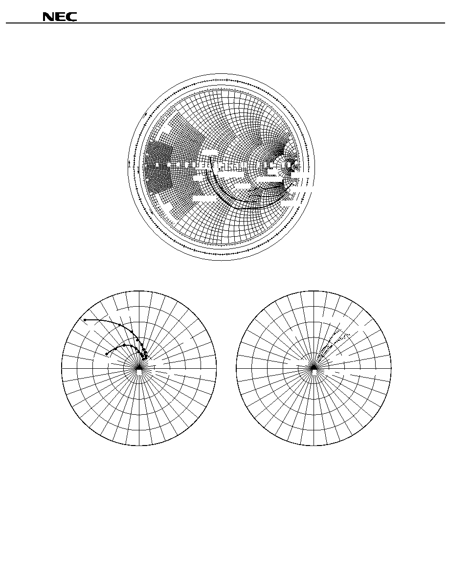
S-PARAMETER
V
CE
= 6.0 V, I
C
= 3.0 mA, Z
O
= 50
f (MHz)
S
11
S
11
S
21
S
21
S
12
S
12
S
22
S
22
200
400
600
800
1000
1200
1400
1600
1800
2000
0.870
0.747
0.628
0.516
0.400
0.327
0.262
0.231
0.205
0.196
24.2
44.6
59.8
75.1
87.7
103.4
118.7
135.5
155.3
170.6
9.193
7.780
7.058
5.675
5.180
4.269
3.950
3.406
3.290
2.867
155.6
136.6
122.1
109.4
99.6
89.8
81.7
74.0
66.4
60.8
0.031
0.040
0.064
0.066
0.090
0.084
0.106
0.105
0.126
0.124
53.6
66.2
54.7
56.0
49.4
47.9
48.5
42.1
46.4
40.9
0.946
0.876
0.816
0.743
0.689
0.654
0.604
0.581
0.548
0.529
12.8
20.7
26.4
30.9
33.0
35.7
37.7
41.5
43.9
47.1
V
CE
6.0 V, I
C
= 10.0 mA, Z
O
= 50
f (MHz)
S
11
S
11
S
21
S
21
S
12
S
12
S
22
S
22
200
400
600
800
1000
1200
1400
1600
1800
2000
0.671
0.458
0.319
.0239
0.172
0.149
0.131
0.132
0.150
0.163
43.5
68.7
83.7
101.9
119.3
141.4
163.0
179.6
160.0
150.1
18.685
12.702
9.895
7.275
6.261
5.038
4.597
3.927
3.743
3.233
137.9
115.2
102.8
92.3
85.1
77.4
71.0
64.8
58.8
54.5
0.023
0.029
0.046
0.049
0.067
0.070
0.088
0.094
0.113
0.115
52.1
62.2
54.4
63.1
58.6
57.9
56.1
54.0
55.3
50.0
0.832
0.710
0.649
0.600
0.578
0.559
0.527
0.514
0.494
0.478
19.0
23.9
26.0
27.5
28.4
30.3
32.5
35.7
38.1
41.6
4
2SC4095
S-PARAMETER
A
N
G
L
E
O
F
R
E
F
L
E
C
T
I
O
N
C
O
E
F
F
C
I
E
N
T
I
N
D
E
G
R
E
E
S
20
30
40
50
00
60
70
80
90
100
110
120
130
140
150
-
160
-
150
-
140
-
130
-
120
-
110
-
100
-
90
-
80
-
70
-
60
-
50
-
40
-
30
-
20
-
10
0
10
0.28
0.22
0.30
0.20
0.32
0.18
0.34
0.16
0.36
0.14
0.38
0.12
0.40
0.10
0.42
0.08
0.44
0.06
0.46
0.04
0.21
0.19
0.17
0.15
0.13
0.11
0.09
0.07
0.05
0.03
0.29
0.31
0.33
0.35
0.37
0.39
0.41
0.43
0.45
0.47
0.02 0.48
0.01
0.49
0
0
0.49
0.01
0.48
0.02
0.47
0.03
0.46
0.04
0.45
0.05
0.44
0.06
0.43
0.07
0.42
0.08
0.41
0.09
0.40
0.10
0.39
0.11
0.38
0.12
0.37
0.13
0.36
0.14
0.35
0.15
0.34
0.16
0.33
0.17
0.32
0.18
0.31
0.19
0.30
0.20
0.29
0.21
0.28
0.22
0.27
0.23
0.26
0.24
0.25
0.25
0.24
0.26
0.23
0.27
W
A
V
E
L
E
N
G
T
H
S
T
O
W
A
R
D
L
O
A
D
W
A
V
E
L
E
N
G
T
H
S
T
O
W
A
R
D
G
E
N
E
R
A
T
O
R
2.0
50
10
6.0
4.0
3.0
1.8
1.6
1.4
1.2
0.9
0.8
0.7
0.6
0.5
0.4
0.3
0.2
0.1
1.0
(
+JX
≠≠≠≠
Z
O
)
0.2
0.4
0.6
0.8
1.0
0.8
0.7
0.6
0.3
0.2
0.1
0.2
1.0
0.8
0.6
0.4
0.2
1.0
0.8
0.6
0.4
0.4
0.5
5.0
10
50
3.0
4.0
1.8
2.0
1.2
1.0
0.9
1.4
1.6
REACTANCE COMPONENT
(
R
≠≠≠≠
Z
O
)
NE
GA
TIV
E
RE
A
CT
A
N
C
E C
OM
P
O
N
E
N
T
P
OS
IT
IV
E
R
E
A
C
TA
N
C
E
CO
M
PO
NE
NT
0.1
0.2
0.3
0.4
0.5
0.6
0.7
0.8
0.9
1.0
1.2
1.4
1.6
1.8
2.0
3.0
4.0
5.0
10
20
0
(
-
JX
≠≠≠≠
Z
O
)
20
20
0.2
0.4
0.6
0.8
1.0
S
11e
, S
22e
-FREQUENCY
S
21e
-FREQUENCY
90
∞
0
∞
30
∞
-
30
∞
60
∞
-
60
∞
180
∞
150
∞
-
150
∞
120
∞
-
120
∞
-
90
∞
4
0
8
12
16
20
S
21e
2GHz
90
∞
0
∞
30
∞
-
30
∞
60
∞
-
60
∞
180
∞
150
∞
-
150
∞
120
∞
-
120
∞
-
90
∞
0.04
0
0.08
0.12 0.16 0.2
S
12e
CONDITION V
CE
= 6 V, I
C
= 10/3 mA, freq. = 0.2 to 2 GHz (Step 200 MHz)
CONDITION V
CE
= 6 V
I
C
= 10/3 mA
freq. = 0.2 to 2 GHz (Step 200 MHz)
S
12e
-FREQUENCY
CONDITION V
CE
= 6 V
I
C
= 10/3 mA
freq. = 0.2 to 2 GHz (Step 200 MHz)
0.2 GHz
0.2 GHz
2 GHz
2 GHz
I
C
= 3 mA
I
C
= 3 mA
I
C
= 10 mA
I
C
= 10 mA
I
C
= 3 mA
I
C
= 3 mA
S
11e
S
22e
I
C
= 10 mA
I
C
= 10 mA
0.2 GHz
0.2 GHz
2GHz
5
2SC4095
RECOMMENDED SOLDERING CONDTITIONS
The following conditions (see table below) must be met then soldering this product. Please consult with our sales
offices in case other soldering process is used, or in case soldering is done under different contions.
TYPES OF SURFACE MOUNT DEVICE
For more details, refer to our document "SMT MANUAL" (IEI-1207).
2SC4095
Soldering process
Soldering conditions
Symbol
Infrared ray reflow
Peak package's surface temperature: 230
C or below,
Reflow time:
30 seconds or below (210
C or higher),
Number of reflow process:
1, Exposure limit*: None
IR30-00-1
VPS
Peak package's surface temperature: 215
C or below,
Reflow time:
40 seconds or below (200
C or higher),
Number of reflow process:
1, Exposure limit*: None
VP15-00-1
Wave soldering
Solder temperature:
260
C or below,
Flow time:
10 seconds or below,
Number of reflow process:
1, Exposure limit*: None
WS60-00-1
Partial heating method
Terminal temperature:
300
C or below,
Flow time:
3 seconds or below,
Exposure limit*:
None
*: Exposure limit before soldering after dry-pack package is opened.
Storage conditions: 25
C and relative humidity at 65 % or less.
Note: Do not apply more than a single process at once, except for "Partial heating method".