©
1989
DATA SHEET
GaAs INTEGRATED CIRCUIT
µ
PG110P
DESCRIPTION
The
µ
PG110P is a GaAs monolithic integrated circuit designed as a wide band amplifier from 2 to 8 GHz. And
the device is available in chip form. The
µ
PG110P is suitable for the gain stage required high gain characteristic of
the microwave communication system and the measurement equipment.
FEATURES
∑
Ultra wide band : 2 to 8 GHz
∑
High Power Gain : G
P
= 15 dB TYP.
@f = 2 to 8 GHz
∑
Medium Power
: P
O(1 dB)
= +14 dBm TYP. @f = 2 to 8 GHz
ORDERING INFORMATION
PART NUMBER
FORM
µ
PG110P
Chip
ABSOLUTE MAXIMUM RATINGS (T
A
= 25
∞
C)
Supply Voltage
V
DD
+10
V
Input Voltage
V
IN
≠5 to +0.6
V
Input Power
P
in
+10
dBm
Total Power Dissipation
P
tot
*
1
1.5
W
Operating Temperature
T
opr
*
2
≠65 to +125
∞
C
Storage Temperature
T
stg
≠65 to +125
∞
C
*1 Mounted with AuSn hard solder
*2 The temperature of base material beside the chip
RECOMMENDED OPERATING CONDITIONS (T
A
= 25
∞
C)
Supply Voltage
V
DD
+8
±
0.2
V
Input Power
P
in
≠5
dBm
Document No. P11882EJ2V0DS00 (2nd edition)
(Previous No. ID-2454)
Date Published September 1996 P
Printed in Japan
2 to 8 GHz WIDE BAND AMPLIFIER CHIP
µ
PG110P
2
ELECTRICAL CHARACTERISTICS (T
A
= 25
∞
C)
*3
CHARACTERISTIC
SYMBOL
MIN.
TYP.
MAX.
UNIT
TEST CONDITIONS
Supply Current
I
DD
65
135
180
mA
V
DD
= +8 V
Power Gain
G
P
12
15
dB
f = 2 to 8 GHz
Gain Flatness
G
P
±
1.5
dB
Input Return Loss
RL
in
6
10
dB
Output Return Loss
RL
out
7
10
dB
Isolation
ISL
30
40
dB
Output Power at 1 dB
P
O(1 dB)
10
14
dBm
Gain Compression Point
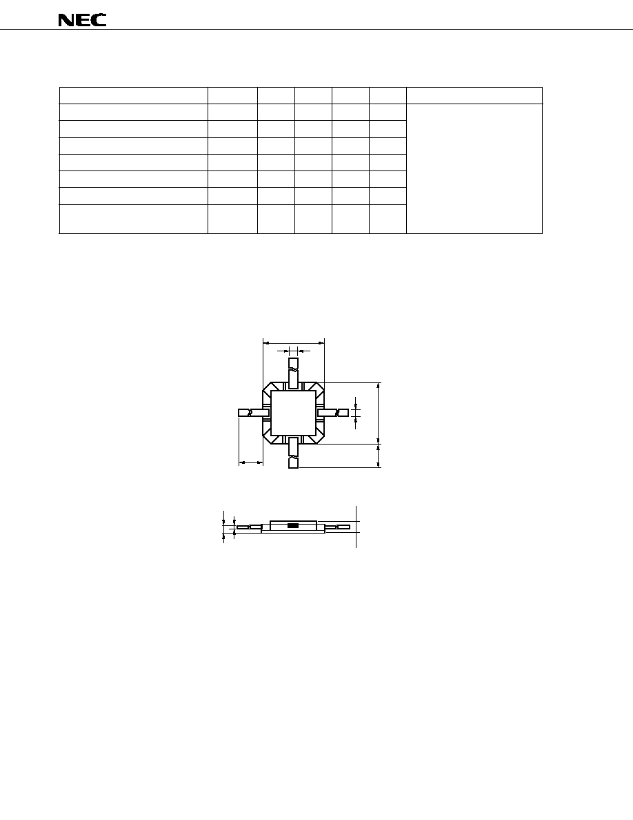
*3 These characteristics are based on performance of devices mounted in the standard package shown in Fig. 1.
Fig. 1 4 pin Ceramic Package
4.5 MAX.
4.6 MAX.
4.1 MIN.
0.4 ± 0.06
4.1 MIN.
1.48 MAX.
0.1 ± 0.06
0.7
+0.2 ≠0.1
0.6
± 0.06
Top View
µ
PG110P
3
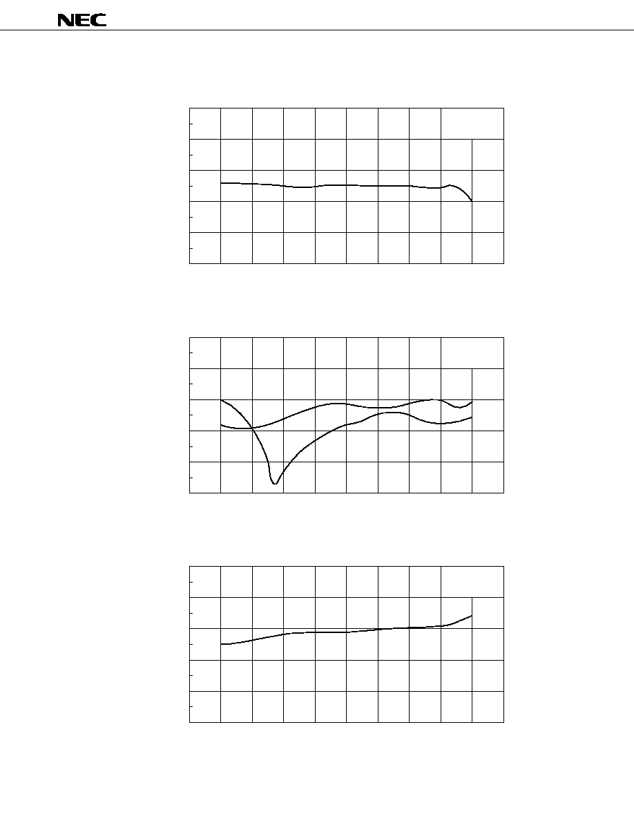
TYPICAL CHARACTERISTICS (T
A
= 25
∞
C)
*4
30
20
10
0
0
1
2
3
4
5
6
7
8
9
10
f - Frequency - GHz
G
P
- Power Gain - dB
0
≠10
≠20
≠30
0
1
2
3
4
5
6
7
8
9
10
f - Frequency - GHz
RL
in
- Input Return Loss - dB
RL
out
- Output Return Loss - dB
≠20
≠40
≠60
≠80
0
1
2
3
4
5
6
7
8
9
10
f - Frequency - GHz
ISL - Isolation - dB
POWER GAIN vs. FREQUENCY
INPUT RETURN LOSS vs. FREQUENCY
ISOLATION vs. FREQUENCY
0
V
DD
= +8 V
I
DD
= 132 mA
V
DD
= +8 V
I
DD
= 132 mA
RL
in
RL
out
V
DD
= +8 V
I
DD
= 132 mA
µ
PG110P
4
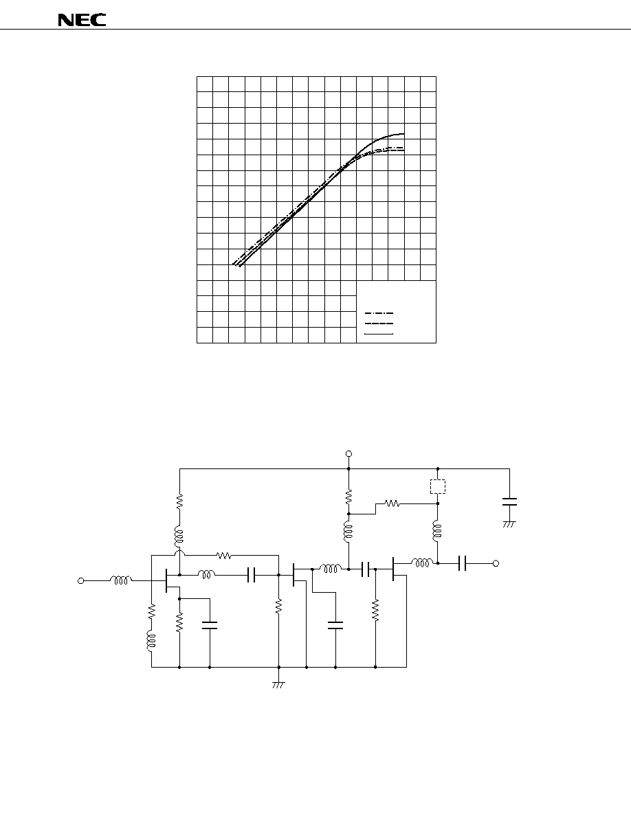
20
10
0
≠20
≠10
0
10
OUTPUT POWER vs. INPUT POWER
P
out
- Output Power - dBm
P
in
- Input Power - dBm
V
DD
= +8 V
I
DD
= 132 mA
f = 2 GHz
f = 5 GHz
f = 8 GHz
*4 These characteristics are measured for device mounted in the standard package shown in Fig. 1.
EQUIVALENT CIRCUIT
R
G1
L
G1
IN
L
in
R
S1
C
S
L
L1
R
L1
R
F1
C
1
R
G2
L
1
L
2
L
L2
R
G3
C
2
C
4
R
F2
Active
Load
C
RF
L
L3
OUT
C
3
L
3
V
DD
R
L2
µ
PG110P
5
RECOMMENDED CHIP ASSEMBLY CONDITIONS
Die Attachment
Atmosphere
: N
2
gas
Temperature : 320
±
5
∞
C
AuSn Preform : 0.5
◊
0.5
◊
0.05
t
(mm), 1 pce.
* The hard solder such as AuSi or AuGe which has higher melting point than AuSn should not
be used.
Base Material : CuW, Cu, KV
* Other material should not be used.
Epoxy Die Attach is not recommended.
Bonding
Machine
: TCB
* USB is not recommended
Wire
: 30
µ
m diameter Au wire
Temperature : 260
±
5
∞
C
Strength
: 31
±
3 g
Atmosphere
: N
2
gas
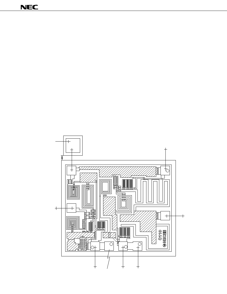
Chip Bonding Diagram
V
DD
50 to
100 m
µ
200 to 500 m
µ
V
DD
GND
less than 300 m
µ
5
4
3
2
1
500 to
1 000 m
µ
IN
GND
GND
GND
GND
OUT
not used
less than 200 m
µ
200 to
500 m
µ