
The information in this document is subject to change without notice. Before using this document, please
confirm that this is the latest version.
Not all devices/types available in every country. Please check with local NEC representative for
availability and additional information.
1998
©
Document No. D15594EJ2V0DS00 (2nd edition)
Date Published April 2002 N CP(K)
Printed in Japan
DARLINGTON POWER TRANSISTOR
2SC4351
NPN SILICON EPITAXIAL TRANSISTOR (DARLINGTON CONNECTION)
FOR HIGH-SPEED SWITCHING
DATA SHEET
2002
The 2SC4351 is a high-speed Darlington power transistor. This
transistor is ideal for high-precision control such as PWM control for
pulse motors or blushless motor of OA and FA equipment.
FEATURES
∑ Mold package that does not require an insulating board or
insulation bushing
∑ On-chip C to B constant voltage diode for surge voltage
absorption
∑ On-chip C to E reverse diode
∑ Fast switching speed
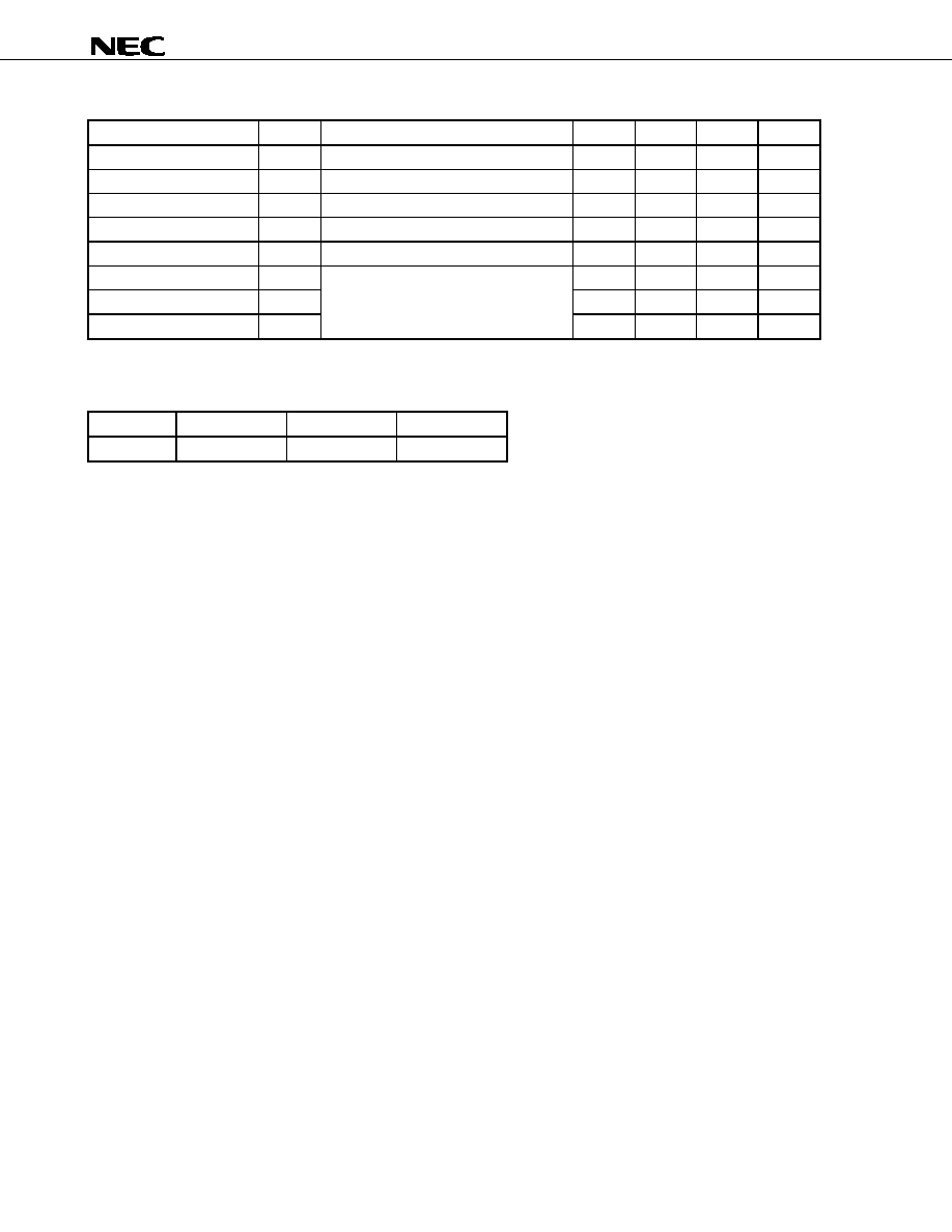
ABSOLUTE MAXIMUM RATINGS (Ta = 25
∞
∞
∞
∞C)
Parameter
Symbol
Ratings
Unit
Collector to base voltage
V
CBO
60
± 10
V
Collector to emitter voltage
V
CEO
60
± 10
V
Emitter to base voltage
V
EBO
8.0
V
Collector current (DC)
I
C(DC)
±5.0
A
Collector current (pulse)
I
C(pulse)
*
±10
A
Base current (DC)
I
B(DC)
0.5
A
Total power dissipation
P
T
(Tc = 25
∞C)
20
W
Total power dissipation
P
T
(Ta = 25
∞C)
2.0
W
Junction temperature
T
j
150
∞C
Storage temperature
T
stg
-55 to +150
∞C
* PW
10 ms, duty cycle 50%
PACKAGE DRAWING (UNIT: mm)
Electrode Connection
1. Base
2. Collector
3. Emitter
Data Sheet D15594EJ2V0DS
2
2SC4351
ELECTRICAL CHARACTERISTICS (Ta = 25
∞
∞
∞
∞C)
Parameter
Symbol
Conditions
MIN.
TYP.
MAX.
Unit
Collector cutoff current
I
CBO
V
CB
= 40 V, I
E
= 0
0.5
µA
DC current gain
h
FE1
*
V
CE
= 2.0 V, I
C
= 2.0 A
2,000
20,000
DC current gain
h
FE2
*
V
CE
= 2.0 V, I
C
= 4.0 A
500
Collector saturation voltage
V
CE(sat)
*
I
C
= 2.0 A, I
B
= 2.0 mA
1.5
V
Base saturation voltage
V
BE(sat)
*
I
C
= 2.0 A, I
B
= 2.0 mA
2.0
V
Turn-on time
t
on
0.7
µs
Storage time
t
stg
2.5
µs
Fall time
t
f
I
C
= 2.0 A, I
B1
=
-I
B2
= 2.0 mA,
R
L
= 25
, V
CC
50 V
Refer to the test circuit.
0.6
µs
* Pulse test PW
350
µs, duty cycle 2%
h
FE
CLASSIFICATION
Marking
M
L
K
h
FE1
2,000 to 5,000
4,000 to 10,000
8,000 to 20,000

Data Sheet D15594EJ2V0DS
3
2SC4351
TYPICAL CHARACTERISTICS (Ta = 25
∞
∞
∞
∞C)
Co
l
l
e
c
to
r
Cu
r
r
e
n
t
I
C
(
A
)
Collector to Emitter Voltage V
CE
(V)
Case Temperature T
C
(
∞
C)
Case Temperature T
C
(
∞
C)
T
o
ta
l
P
o
we
r
Dis
s
i
p
a
ti
o
n
P
T
(W
)
I
C
D
e
r
a
ti
n
g
d
T
(
%
)
Co
l
l
e
c
to
r
Cu
r
r
e
n
t
I
C
(
A
)
Co
l
l
e
c
to
r
Cu
r
r
e
n
t
I
C
(
A
)
Base to Emitter Voltage V
BE
(V)
Collector to Emitter Voltage V
CE
(V)
T
r
an
si
en
t
T
h
e
r
ma
l
R
e
si
st
a
n
c
e
R
t
h
(j
-c
)
(
∞
C/W
)
Pulse Width PW (ms)

